

SANYO LA7170M Datasheet
Overview
The LA7170M is a UHF band RF modulator whose builtin RF oscillator and mixer make it a single-chip RF
modulator solution. It also supports image positivity
modulation and AM sound modulation for SECAM
systems.
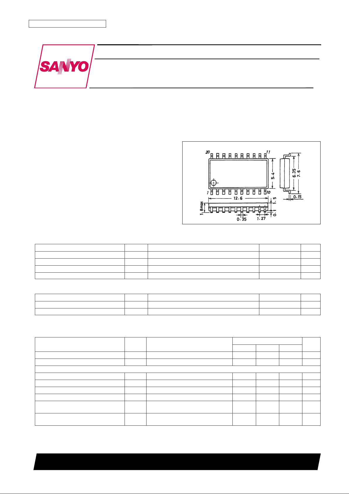
Package Dimensions
unit: mm
3036B-MFP20
Monolithic linear IC
43098HA (OT) No. 5675-1/8
SANYO: MFP20
[LA7170M]
SANYO Electric Co.,Ltd. Semiconductor Bussiness Headquarters
TOKYO OFFICE Tokyo Bldg., 1-10, 1 Chome, Ueno, Taito-ku, TOKYO, 110-8534 JAPAN
RF Modulator for UHF Band (Supports SECAM)
LA7170M
Ordering number : EN5675
Parameter Symbol Conditions Ratings Unit
Maximum supply voltage V
CC
max 7V
Allowable power dissipation Pd max Ta ≤ 75°C 250 mW
Operating temperature Topr –20 to +75 °C
Storage temperature Tstg –55 to +150 °C
Specifications
Maximum Ratings at Ta = 25°C
Parameter Symbol Conditions Ratings Unit
Recommended operating voltage V
CC
5.0 V
Operating supply voltage range V
CC
op 4.5 to 5.5 V
Operating Conditions at Ta = 25°C
Parameter Symbol Conditions
Ratings
Unit
min typ max
Current drain 1 I
CC
1 With no input 24 30 36 mA
Regulator voltage Vreq With no input 3.7 3.9 4.1 V
[RF Output Level] (S19A: A, S19B: A)
Picture carrier output P With no input, with 50 Ω terminator 77 79.5 82 dBµ
Sound carrier output ratio P/S Ratio of levels at fp and fp+fs 12.5 15 17.5 dB
Sound second harmonic distortion P/S2 Ratio of levels at fp and fp+2fs 52 62 dB
Sound third harmonic distortion P/S3 Ratio of levels at fp and fp+3fs 58 68 dB
Chrominance beat P/CB
Ratio of P above to chrominance beat for
65 75 dB
V
IN
= 0.4 Vp-p with 4.43-MHz sine wave input
Picture harmonic distortion P/V2
Ratio of P above to level at fp+2 MHz for
50 62 dB
VIN= 1 Vp-p with 1-MHz sine wave input
Operating Characteristics at Ta = 25°C, VCC= 5 V, Unless otherwise specified, fp = 591.25 MHz, fs = 5.5 MHz,
S9: ON, S10: B, S19A: B, S19B: B
Continued on next page.
No. 5675-2/8
LA7170M
Continued from preceding page.
Parameter Symbol Conditions
Ratings
Unit
min typ max
[Picture]
Picture modulation mp V
IN
= 1 Vp-p, 100% white 73 80 87 %
Maximum picture modulation mp max V
IN
= 1.5 Vp-p, 100% white 88 93 98 %
SYNC compression ∆(S/V) V
IN
= 1 Vp-p,
100%
white
{1–(S/V)(3/7)} × 100
1.5 5 %
Differential gain DG V
IN
: 5-stair step, mp = 80%, at fourth step 2 5 %
Differential phase DP V
IN
: 5-stair step, mp = 80%, at fourth step –6 0 +6 deg
SECAM picture modulation mp SCM V
IN
= 1 Vp-p, 100% white S10 : a 88 93 98 %
TSG picture modulation mp TSG S9 : off 70 80 90 %
TSG SV ratio V/S S9 : off 6.3/3.7 6.8/3.2 7.3/2.7
TSG horizontal period TS S9 : off 63.7 64.0 64.3 µs
TSG synchronization pulse width HS S9 : off 3.6 4.0 4.4 µs
TSG white signal width HV S9 : off 3.6 4.0 4.4 µs
TSG first white rising edge TV1 S9 : off 22 24 26 µs
TSG second white rising edge TV2 S9 : off 38 40 42 µs
[Sound]
FM sound modulation Rank A 73 81 89 %
Rank B
ms FM
81 90 99 %
Rank C 90 100 110 %
Rank D 99 110 121 %
Rank E 109 121 133 %
Interchannel FM sound modulation ratio ∆ms FM ms FM ratio with S10: off 0.93 0.98 1.03
FM sound distortion THD FM
S10: b/off; A
IN
= 1 V
p-p
with 1-kHz sine
0.3 1.0 %
wave input
S10: b/off; V
IN
= 1 Vp-p color bar; AINwith
FM sound signal-to-noise ratio S/NFM 1-kHz sine wave input; ratio of level at A
IN
= 43 55 dB
1 Vp-p to that at A
IN
= 0 Vp-p
Maximum FM modulation ms max
Maximum modulation possible with S10:
400 %
b/off and sound distortion ratio within 3%
AM sound modulation ms AM
S10: a; A
IN
= 1 Vp-p with 1-kHz sine wave
43 50 57 %
input
AM sound distortion ratio THD AM
S10: a; AIN= 1 Vp-p with 1-kHz sine wave
0.5 2 %
input
S10: a; V
IN
= 1 Vp-p color bar; AINwith 1-kHz
AM sound signal-to-noise ratio S/N AM sine wave input; ratio of level at A
IN
= 1 Vp-p 42 47 dB
to that at A
IN
= 0 Vp-p
AIN= 1.66 Vp-p with 1-kHz sine wave input;
100% modulation: ±50 kHz; S10: b
Note: A
IN
= 1 Vp-p normally produces 60%
modulation.
Note: The AM sound items refer to direct AM detection from the sound carrier (fp + sound intercarrier). This device requires the special care associated with
all high-frequency devices.
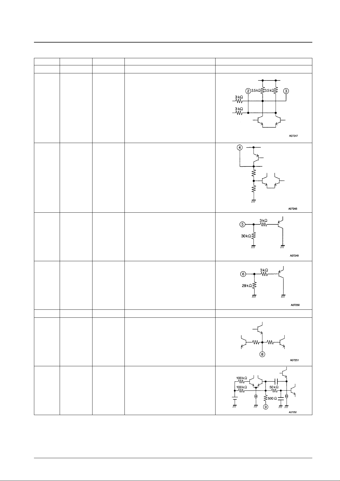
Pin No. Symbol Pin Voltage Pin Description Equivalent Circuit
5.0
VCCfor baseband circuits
1
VCC1
No. 5675-3/8
LA7170M
Pin Functions
3.9
Connect tank circuits between these pins and the
REG pin.
2
3
TANK1
TANK2
3.9 Regulator output4 REG
0 FM sound input5 FM AUDIO IN
0 AM sound input6 AM AUDIO IN
0 Ground for baseband circuits7 GND1
3.0 Picture input. Clamp at SYNC tip.8 VIDEO IN
2.6
(open)
Ground this pin through a 500-kHz oscillator.
Open : TSG ON
GND : TSG OFF
9 RES
Continued on next page.
 Loading...