

Page 1
LA7161V
Ordering number : EN6081
VHF Band RF Modulator
Monolithic Linear IC
SANYO Electric Co.,Ltd. Semiconductor Bussiness Headquaters
TOKYO OFFICE Tokyo Bldg., 1-10, 1 Chome, Ueno, Taito-ku, TOKYO, 110-8534 JAPAN
N1098RM (KT) No.6081-1/5
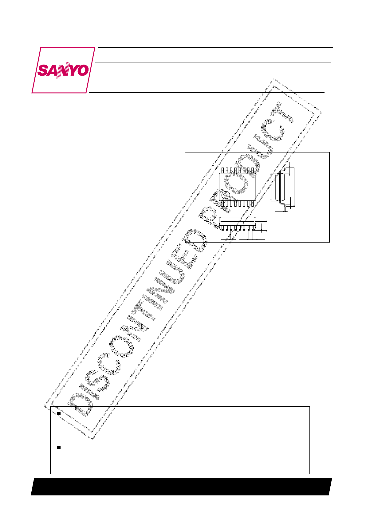
Package Dimensions
unit: mm
3178-SSOP16
[LA7161V]
SANYO : SSOP16
18
916
6.4
0.5
4.4
5.4
0.1
1.6max
1.0
0.650.22
0.43
0.15
Functions
• RF VCO
• RF mixer
• RF buffer
• Video clamp
• White clip
• Audio FM
• 4V regulator
• Reference OSC
Overview
The LA7161V is an RF modulator which generates, from a
baseband video and audio signal, PLL frequency
synthesized RF TV channel signal in VHF band.
Features
• 5V operation.
• PLL synthesized RF VCO (US : 3ch, 4ch, JPN : 1ch, 2ch
, TWN : 13ch only), channel selection accomplished
using two pins.
• PLL synthesized (4.5MHz frequency) and tankless audio
FM.
• The 4 or 3.58MHz (color subcarrier) reference frequency
for PLL can either be generated internally or input from
an external source.
Any and all SANYO products described or contained herein do not have specifications that can handle
applications that require extremely high levels of reliability, such as life-support systems, aircraft's
control systems, or other applications whose failure can be reasonably expected to result in serious
physical and/or material damage. Consult with your SANYO representative nearest you before using
any SANYO products described or contained herein in such applications.
SANYO assumes no responsibility for equipment failures that result from using products at values that
exceed, even momentarily, rated values (such as maximum ratings, operating condition ranges, or other
parameters) listed in products specifications of any and all SANYO products described or contained
herein.
Page 2
LA7161V
No.6081-2/5
Operating Characteristics
at Ta=25°C, VCC=5V, US 3ch unless otherwise specified
Parameter Symbol Conditions
Ratings
min typ max
Unit
Supply current 1 I
CC
1 No signal, pin 6, high 26 37 48 mA
Supply current 2 I
CC
2 No signal, pin 6, low 17 25 23 mA
Regulator voltage Vreg No signal 3.7 3.9 4.1 V
ANT SW driver V
ANT
Pin 6, high, 220Ω load 3.2 3.5 3.8 V
RF output US P
US
No signal *2 84 87 90 dBµ
RF output JP P
JP
No signal, JPN 1ch *2 83.5 86.5 89.5 dBµ
RF output TWN P
TW
No signal, TWN 13ch *2 83 86 89 dBµ
P/S ratio P/S S : fp+4.5MHz 13.5 16 18.5 dB
4.5MHz 2nd harmonics P/S2 S2 : fp+2
×4.5MHz 50 65 – dB
4.5MHz 3rd harmonics P/S3 S3 : fp+3×4.5MHz 50 55 – dB
920kHz beat P/CB V
IN
=3.58MHz, 0.6Vp-p 65 72 – dB
CB : fp+920kHz
Video harmonics P/V2 V
IN
=1MHz, 1Vp-p 45 65 – dB
V2 : fp+2MHz
Video modulation Mp V
IN
=Stair step, 1Vp-p 75 80 85 %
White clip level WCL V
IN
=Stair step, 1.5Vp-p 88 93 98 %
Differential gain DG V
IN
=Stair step, 1Vp-p –5 – +5 %
Differential phase DP V
IN
=Stair step, 1Vp-p –5 – +5 Deg
Audio modulation M
S
AIN=1kHz, 1Vp-p *3 90 100 110 %
Maximum audio modulation M
S
max THD<3% 400 – – %
Audio THD THD A
IN
=1kHz, 1Vp-p – 0.4 2 %
Audio S/N S/N A
IN
=1kHz, 1Vp-p 45 52 – dB
V
IN
=Color bar, 1Vp-p
Specifications
Maximum Ratings
at Ta=25°C
Parameter Symbol Conditions Ratings Unit
Maximum supply voltage V
CC
max 7 V
Allowable power dissipation Pd max * 350 mW
Operating temperature Topr –20 to +75 °C
Storage temperature Tstg –55 to +150 °C
Note : When mounted on a glass epoxy resin circuit board (114.3mm × 76.1mm × 1.6mm)
Operating Conditions
at Ta=25°C
Parameter Symbol Conditions Ratings Unit
Recommended supply voltage V
CC
5V
Operating voltage range V
CC
op 4.5 to 5.5 V
Notes *2 : Measure the pin RF OUT with a spectrum analyzer of 50Ω input impedance and add 9.5 dB to that value.
*3 : 100%=±25kHz modulation.
Page 3

LA7161V
No.6081-3/5
Test Circuit (US CH)
1516 14 13 12 11 10 9
1234 5678
A11862
RF OUT
0.1µF
100Ω
100pF
0.1µF
100pF
2200pF
+VCC (5V)
AUDIO IN
18pF
6800pF
0.022µF
0.1µF
1500pF
15pF
0.33µF
0.1µF
0.047µF
0.1µF
3.6kΩ
56kΩ
10kΩ
47kΩ
470Ω
470Ω
10kΩ
4MHz
VIDEO IN
ANT.SW
DRIVE
LA7161V
RF OFF
(Hi : RF work)
CHANNEL
Citizen
CMR-310
220Ω
1516 14 13 12 11 10 9
1234567 8
A11861
BIAS
REG
4.0V
RF
OSC
ANT SW
DRIVER
RF
MIXER
PLL
FM
OSC
WHITE
CLIP
CARRIER
OFF SW
REF
OSC
PLL
CHANNEL
CLAMP
BUFBUF
PS
ADJ
AUDIO IN
FM LPF
GND
VIDEO IN
CARR OFF
IN XTAL
CH
REG
RF OUT
ANT DRV
V
CC
1
RF LPF
V
CC
2
OSC2
OSC1
OFF
OFF
Equivalent Circuit Block Diagram
Page 4

LA7161V
No.6081-4/5
Sample Application Circuit (US, JPN CH)
Sample Application Circuit (TWN CH)
1516 14 13 12 11 10 9
1234 5678
A11863
RF OUT
0.1µF
820Ω
82Ω
100pF
0.1µF
100pF
2200pF
+VCC (5V)
AUDIO IN
XXP
US:18pF
JPN:15pF
6800pF
0.022µF
0.1µF
1500pF
15pF
0.33µF
0.1µF
0.047µF
0.1µF
3.6kΩ
56kΩ
47kΩ
470Ω
470Ω
10kΩ
4MHz
Citizen
CMR-310
VIDEO IN
ANT.SW
DRIVE
LA7161V
CHANNEL
OPEN:US 3CH
GND:US 4CH
OPEN:JPN 1CH
GND:JPN 2CH
RF OFF
(Low ACTIVE)
8.2kΩ
(JPN:SHORT)
2.7kΩ
(JPN:REMOVE)
10kΩ
~∞
1516 14 13 12 11 10 9
1234 5678
A11864
RF OUT
0.1µF
750Ω
82Ω
100pF
0.1µF
100pF
2200pF
+VCC (5V)
AUDIO IN
18pF
6800pF
0.022µF
0.1µF
1500pF
15pF
0.33µF
0.1µF
0.047µF
0.1µF
3.6kΩ
56kΩ
270kΩ
47kΩ
470Ω
470Ω
10kΩ
4MHz
(3.58MHz)
Citizen
CMR-310
VIDEO IN
ANT.SW
DRIVE
LA7161V
4MHz:OPEN
fSC=3.58MHz:GND
RF OFF
(Low ACTIVE)
REF
Page 5

LA7161V
PS No.6081-5/5
Channel
Reference
Frequency (MHz)
Voltage of PIN8
(V)
A Resistor between
PIN7 and GND (kΩ)
A Resistor between
PIN8 and GND (kΩ)
US3
4.0 over 4.2 W/O W/O
3.58 same as above W W/O
US4
4.0 2.7 to 3.8 W/O W/O
3.58 same as above W W/O
JPN1
4.0 1.2 to 2.3 W/O W/O
3.58 same as above W W/O
JPN2
4.0 under 0.8 W/O W/O
3.58 same as above W W/O
TWN13
4.0 1.2 to 2.3 W/O W
3.58 under 0.8 W/O W
Application for Channel Selection
Specifications of any and all SANYO products described or contained herein stipulate the performance,
characteristics, and functions of the described products in the independent state, and are not guarantees
of the performance, characteristics, and functions of the described products as mounted in the customer's
products or equipment. To verify symptoms and states that cannot be evaluated in an independent device,
the customer should always evaluate and test devices mounted in the customer's products or equipment.
SANYO Electric Co., Ltd. strives to supply high-quality high-reliability products. However, any and all
semiconductor products fail with some probability. It is possible that these probabilistic failures could
give rise to accidents or events that could endanger human lives, that could give rise to smoke or fire,
or that could cause damage to other property. When designing equipment, adopt safety measures so
that these kinds of accidents or events cannot occur. Such measures include but are not limited to protective
circuits and error prevention circuits for safe design, redundant design, and structural design.
In the event that any or all SANYO products(including technical data,services) described or
contained herein are controlled under any of applicable local export control laws and regulations,
such products must not be exported without obtaining the export license from the authorities
concerned in accordance with the above law.
No part of this publication may be reproduced or transmitted in any form or by any means, electronic or
mechanical, including photocopying and recording, or any information storage or retrieval system,
or otherwise, without the prior written permission of SANYO Electric Co. , Ltd.
Any and all information described or contained herein are subject to change without notice due to
product/technology improvement, etc. When designing equipment, refer to the "Delivery Specification"
for the SANYO product that you intend to use.
Information (including circuit diagrams and circuit parameters) herein is for example only ; it is not
guaranteed for volume production. SANYO believes information herein is accurate and reliable, but
no guarantees are made or implied regarding its use or any infringements of intellectual property rights
or other rights of third parties.
This catalog provides information as of November, 1998. Specifications and information herein are subject
to change without notice.
 Loading...