

SANYO LA7160M Datasheet
LA7160M
Ordering number : EN5570B
VHF Band RF Modulator
Monolithic Linear IC
SANYO Electric Co.,Ltd. Semiconductor Bussiness Headquarters
TOKYO OFFICE Tokyo Bldg., 1-10, 1 Chome, Ueno, Taito-ku, TOKYO, 110 JAPAN
13098HA (KT) / N2897HA (KT) / 73196RM No.5570-1/3
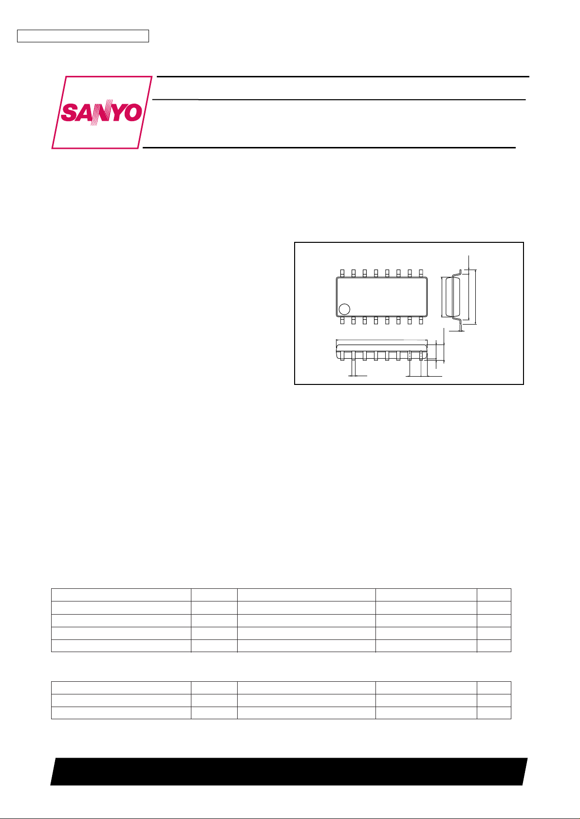
Package Dimensions
unit: mm
3035A-MFP16 (SOP16)
[LA7160M]
SANYO : MFP16
1
16
8
9
10.1
0.15
0.6051.27
0.35
0.1
1.8max
1.5
0.625
4.4
5.15
6.4
Overview
The LA7160M is an RF modulator which generates, from a
baseband video and audio signal, PLL frequency
synthesized RF TV channel signal in VHF band.
Features
• 5V operation.
• PLL synthesized RF VCO (US : 3ch, 4ch, JPN : 1ch, 2ch
only), channel selection accomplished using a single pin.
• PLL synthesized and tankless audio FM.
• The 4 or 3.58MHz (color subcarrier) reference frequency
for PLL can either be generated internally or input from
an external source.
• Package : MFP16 (SOP16)
Functions
• RF VCO
• RF mixer
• RF buffer
• Video clamp
• White clip
• Audio FM
• 4V regulator
• Reference OSC
Specifications
Maximum Ratings
at Ta=25°C
Parameter Symbol Conditions Ratings Unit
Maximum supply voltage V
CC
max 7 V
Allowable power dissipation Pd max 250 mW
Operating temperature Topr –20 to +75 °C
Storage temperature Tstg –55 to +150 °C
Operating Conditions at Ta=25°C
Parameter Symbol Conditions Ratings Unit
Recommended supply voltage V
CC
5V
Operating voltage range V
CC
op 4.5 to 5.5 V
LA7160M
No.5570-2/3
Operating Characteristics at Ta=25°C, V
CC
=5V
Parameter Symbol Conditions
Ratings
min typ max
Unit
Supply current 1 I
CC
1 No signal, pin 6, high 20 28 36 mA
Supply current 2 I
CC
2 No signal, pin 6, low 13 18 23 mA
ANT SW driver ANT Pin 6, high 3.2 3.5 3.8 V
RF output US P
US
No signal 89 92 95 dBµ
RF output JP P
JP
No signal 89 92 95 dBµ
P/S ratio P/S S : fp+4.5MHz 13.5 16 18.5 dB
4.5MHz 2nd harmonics P/S2 S2 : fp+2
×4.5MHz 50 65 dB
4.5MHz 3rd harmonics P/S3 S3 : fp+3
×4.5MHz 45 55 dB
920kHz beat P/CB V
IN
=3.58MHz, 0.6Vp-p 65 72 dB
CB : fp+920kHz
Video harmonics P/V2 V
IN
=1MHz, 1Vp-p 45 65 dB
V2 : fp+2MHz
Video modulation Mp V
IN
=Stair step, 1Vp-p 75 80 85 %
White clip level WCL V
IN
=Stair step, 1.5Vp-p 88 93 98 %
Differential gain DG V
IN
=Stair step, 1Vp-p –5 +5 %
Differential phase DP V
IN
=Stair step, 1Vp-p –5 +5 Deg
Audio modulation M
S
AIN=1kHz, 1Vp-p 90 100 110 %
Maximum audio modulation M
S
max THD<3% 400 %
Audio THD THD A
IN
=1kHz, 1Vp-p 0.4 2 %
Audio S/N S/N A
IN
=1kHz, 1Vp-p 45 51 dB
V
IN
=Color bar, 1Vp-p
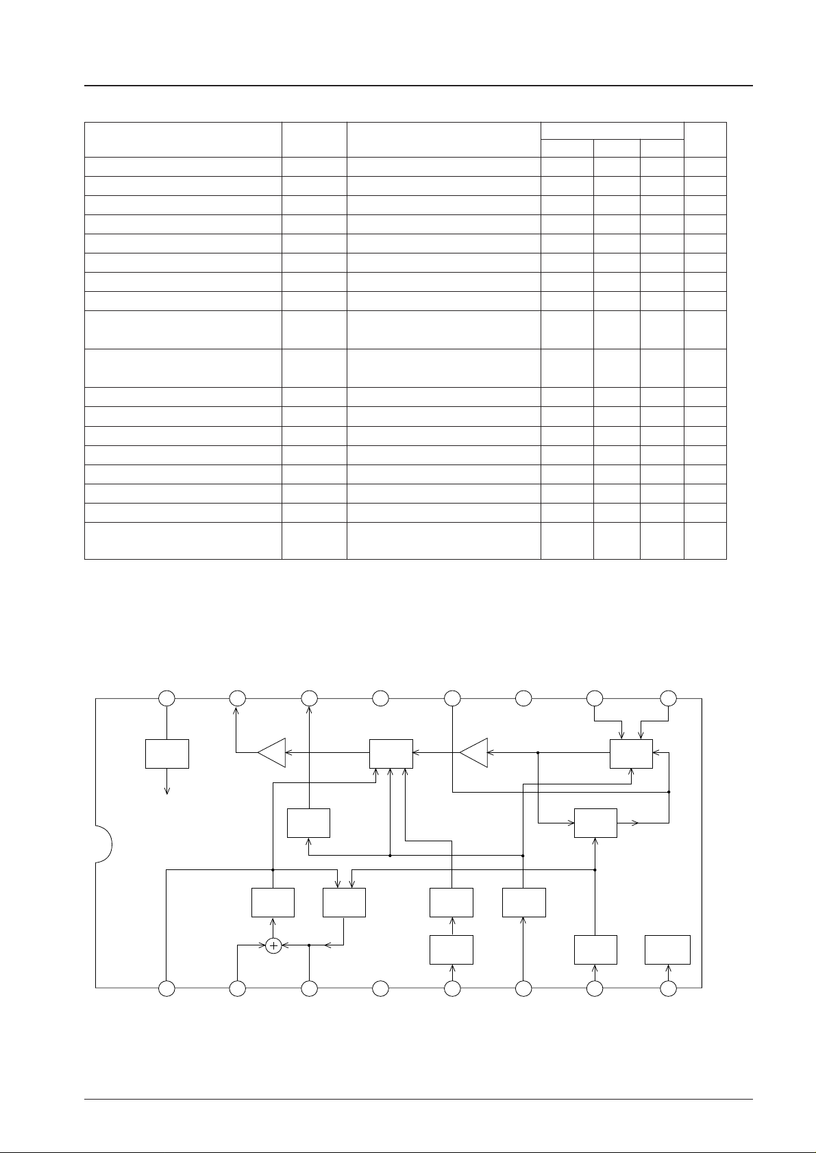
Equivalent Circuit Block Diagram
15
16
14
13
12 11 10 9
1
2 3 4 5 6 7 8
A06397
BIAS
REG
4.0V
RF
OSC
ANT SW
DRIVER
RF
MIXER
PLL
FM
OSC
WHITE
CLIP
CARRIER
OFF SW
REF
OSC
PLL
CHANNEL
CLAMP
BUFBUF
PSADJ
AUDIO IN
FM LPF
GND
VIDEO IN
CARR OFF
IN XTAL
CH
REG
RF OUT
ANT DRV
V
CC
1
RF LPF
V
CC
2
OSC2
OSC1
OFF
OFF
 Loading...