

Page 1
Ordering number : EN4702
22895TH (OT) No. 4702-1/8
Overview
The LA7156 is a switching IC for use with the PAL and
SECAM 21-pin connector interface. The LA7156
integrates video and audio switches in a single chip, and
allows significant block reorganization and integration by
providing function switching outputs with current limiters,
75 Ω video drivers, muting and other functions. The
LA7156 provides a diverse set of functions, including
support for single-wire serial bus control that allows
complex logic to be handled by microprocessor software.
Functions and Features
• Three audio and three video switching systems
• Audio output and video decoder output muting function
• Video input sync chip clamp
• Two 6 dB video amplifier plus 75 Ω driver systems
• VPS decoder output
• FSS output with current limiting
• 5 V regulator built-in
• Serial control
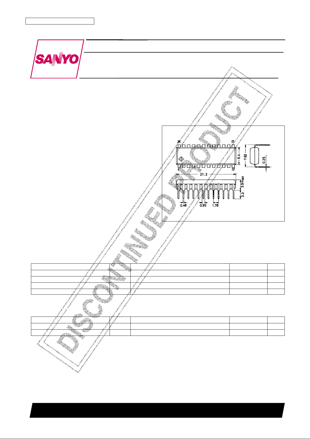
Package Dimensions
unit: mm
3067-DIP24S
SANYO: DIP24S
[LA7156]
LA7156
SANYO Electric Co.,Ltd. Semiconductor Bussiness Headquarters
TOKYO OFFICE Tokyo Bldg., 1-10, 1 Chome, Ueno, Taito-ku, TOKYO, 110-8534 JAPAN
Video and Audio Switch for
PAL-SECAM 21-Pin Interface
Monolithic Linear IC
Specifications
Absolute Maximum Ratings at Ta = 25°C
Operating Conditions at Ta = 25°C
Parameter Symbol Conditions Ratings Unit
Maximum supply voltage V
CC
max 15 V
Allowable power dissipation Pd max Ta ≤ 65°C 800 mW
Operating temperature Topr –20 to +65 °C
Storage temperature Tstg –55 to +150 °C
Parameter Symbol Conditions Ratings Unit
Recommended supply voltage V
CC
9, 12 V
Operating supply voltage range V
CC
op 8 to 13 V
Page 2
Operating Characteristics at Ta = 25°C, VCC= 9 V and 12 V
Note: In the operating characteristics listed above, characteristics items that do not differ between VCC= 9 V and 12 V are listed as the same item.
1. Forced to low when pin 2 is open.
2. Forced to the middle level when pin 20 is open.
No. 4702-2/8
LA7156
Parameter Symbol Conditions min typ max Unit
Current drain I
CC
No input 32 40 48 mA
FSS output high level voltage 1 VHFSS1 V
CC
= 9 V, load resistance: 10 kΩ 7.5 8.9 9.0 V
FSS output low level voltage 1 VLFSS1 V
CC
= 9 V, load resistance: 10 kΩ 0 0.5 V
FSS output high level voltage 2 VHFSS2 V
CC
= 12 V, load resistance: 10 kΩ 10.5 11.9 12.0 V
FSS output low level voltage 2 VLFSS2 V
CC
= 12 V, load resistance: 10 kΩ 0 0.5 V
FSS output cutoff current 1 I
CUTOFF
1
V
CC
= 9 V, the outflow current
9.3 40.0 mA
when the FSS output is grounded
FSS output cutoff current 2 I
CUTOFF
2
V
CC
= 12 V, the outflow current
9.8 40.0 mA
when the FSS output is grounded
[Audio Switch Block]
Total harmonic distortion THD V
IN
= 1 Vrms, f = 1 kHz, R
OUT
= ∞ 0.02 1 %
Maximum output voltage V
O
max The output level when f = 1 kHz and THD = 2% 2 3 Vrms
Output noise voltage V
NO
Rg = 600 Ω, DIN audio filter –100 –90 dBV
Voltage gain A VG
A
The TP6 and TP8 output levels
1.1 1.8 2.5 dB
when V
IN
= 1 Vrms and f = 1 kHz
Interchannel crosstalk A CTA V
IN
= 1 Vrms, f = 1 kHz –90 –70 dB
Muting attenuation A VmuteA V
IN
= 1 Vrms, f = 1 kHz –90 –70 dB
Output offset voltage Vof The offset voltage when the switch has changed state 0 20 mV
Input impedance A Z
IN
A405060kΩ
[Video Switch Block]
Voltage gain V VG
V
The TP2 and TP5 output levels
–10+1dB
when V
IN
= 1 Vp-p and f = 4.43 MHz
Frequency characteristics Vf V
IN
= 1 Vp-p, f = 100 k/7 MHz –1.5 –0.5 +0.5 dB
Second harmonic H2 V
IN
= 1 Vp-p, f = 4.43 MHz –45 –40 dB
Third harmonic H3 V
IN
= 1 Vp-p, f = 4.43 MHz –50 –45 dB
Interchannel crosstalk V CTV V
IN
= 1 Vp-p, f = 4.43 MHz –50 –40 dB
Muting attenuation V VmuteV V
IN
= 1 Vp-p, f = 4.43 MHz –50 –40 dB
Output voltage V
OUT
The TP5 DC voltage with no input 0.7 1.0 V
[Control Block]
Serial control input high level Vsh 4 5 V
Serial control input middle level Vsm 2 3 V
Serial control input low level Vsl 0 1 V
Pin 2 input high level V2H 4 V
CC
V
Pin 2 input low level V2L *102V
Pin 20 input high level V20H 4 V
CC
V
Pin 20 input middle level V20M *223V
Pin 20 input low level V20L 0 1 V
Pin 7 output high level V7H The TP9 DC voltage when SW3 is in the A position 4.5 5.0 5.5 V
Pin 7 output low level V7L The TP9 DC voltage when SW3 is in the B position 0 1 V
Page 3
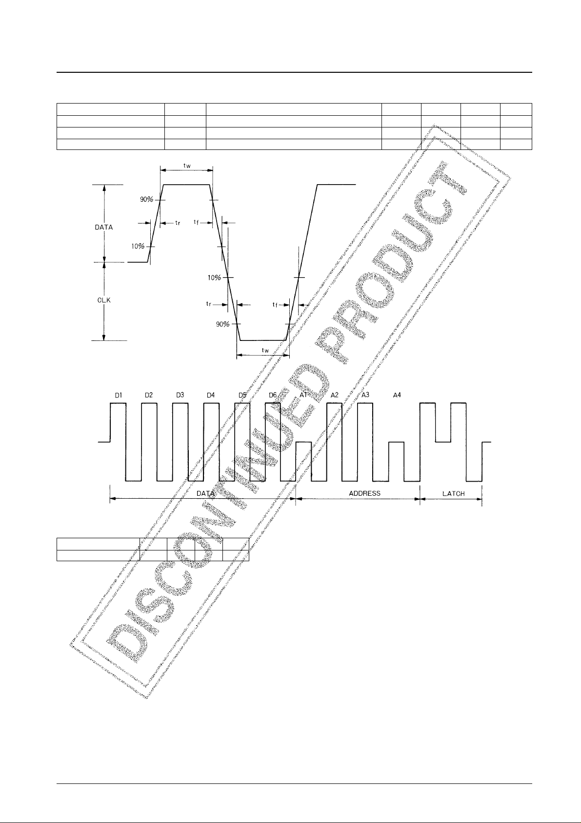
Timing Characteristics
Serial Control Input Specifications
LA7156 Command Address
No. 4702-3/8
LA7156
Parameter Symbol Conditions min typ max Unit
Minimum input pulse width t
W
2µs
Rise time tr 20 µs
Fall time tf 20 µs
Address A1 A2 A3 A4
State L H H L
Page 4

Switch Logic Values Table
The LA7156 provides the following switching control with control of pin 20.
1. Normal mode (when pin 20 is high)
In this mode, the LA7156 functions, including switching, FSS output and muting, can be controlled from the six bits
of serial data transferred from the microprocessor. However, note that the video and audio system switch operate at
the same time in this mode.
Note: 1. All the audio switch and the video SW3 outputs are forcibly muted when DATA6 is high or in muting mode.
2. A.SW indicates the audio system switches and V.SW indicates the video system switches.
2. Preset mode (when pin 20 is middle or low)
This mode uses the LA7156 internally set up logic and the six bits of data are allocated to the VCR operating states
to allow the switch states to be changed.
Serial Data External Input Data
Truth Table
Pin 20: Open or Middle
Note: The previous state is retained even if another switch is changed.
No. 4702-4/8
LA7156
DATA1 Switch state Note DATA4 Switch state Note
H A.SW1-A, V.SW1-A 1, 2 H A.SW3-A, V.SW3-A, pin 7 high 1, 2
L A.SW1-B, V.SW1-B 1, 2 L A.SW3-B, V.SW3-B, pin 7 low 1, 2
DATA2 DATA3 Switch state Note DATA5 FSS output state Note
H L A.SW2-A, V.SW2-A 1, 2 H Output high
L L A.SW2-B, V.SW2-B 1, 2 L Output low
— H A.SW2-C, V.SW2-C 1, 2 DATA6 Muted state Note
H Muted
L Mute released
DATA No. Item H L
D1 Power on/off On Off
D2 VCR/TV VCR TV
D3 Pay CH/Normal CH Pay Normal
D4 EXT/Tuner EXT Tuner
D5 PB/EE PB EE
D6 Mute on/off On Off
Pin No. Item H L
P2 Decoder in Scramble Normal
D1 D2 D3 D4 D5 P2 A.V.SW1 A.V.SW2 A.V.SW3 FSS out Pin 7 out
L ——— —HACALH
L ——— —LACALH
HL— L LHAAALH
HL— LLLACALH
HH— L LHAAAHH
HH— LLLACAHH
HL— H LHABALH
HL— H LL ABALH
HH— H LHABAHH
HH— H LL ABAHH
H ——— HHA* AHH
H ——— HLA* AHH
Page 5

Pin 20: Low
Note: The previous state is retained even if another switch is changed.
Block Diagram and Recommended Circuit Diagram
No. 4702-5/8
LA7156
D1 D2 D3 D4 D5 P2 A.V.SW1 A.V.SW2 A.V.SW3 FSS out Pin 7 out
L ——— —HBABHL
L ——— —LBABL L
HLLLLHBCBHL
HLLLLLACBLL
HHLL LHACAHH
HHLL LLACAHH
HLHL LHAAALH
HLHL LLACALH
HHHL LHAAAHH
HHHL LLACAHH
HL— H LHAABHL
HL— H LL ABBL L
HH— H LHAABHL
HH— H LL ABBHL
H ——— HH A**H *
H ——— HL A**H *
Page 6

Test Circuit
Input and Output Pin Circuit Diagrams
Unit (Resistance: Ω, Current source: A)
No. 4702-6/8
LA7156
Pin No. Symbol I/O circuit DC voltage Note
1
3
5
24
2
4
6
A
IN
1
A
IN
2
A
IN
3
A
IN
4
DEC IN
FSS OUT
V
CC
1/2 VCC+ 0.7 V
V
CC
– 0.2 V
Continued on next page.
Page 7

Continued from preceding page.
Unit (Resistance: Ω, Current source: A)
No. 4702-7/8
LA7156
Pin No. Symbol I/O circuit DC voltage Note
7
8
10
12
13
9
11
14
17
15
16
18
SW3 CTL OUT
V
IN
1
V
IN
2
V
IN
3
V
IN
4
DRIVER V
CC
DRIVER GND
V
OUT
1
V
OUT
2
V
OUT
3
V
OUT
4
GND
External connection
Signal processing IC connection
Signal processing IC connection
H: 5.0 V
L: 0 V
2.5 V
1.6 V
1.6 V
1.6 V
Page 8

PS No. 4702-8/8
LA7156
Continued from preceding page.
Unit (Resistance: Ω, Current source: A)
Pin No. Symbol I/O circuit DC voltage Note
19
20
21
23
22
D/C IN
MODE CTL IN
A
OUT
1
A
OUT
2
A
OUT
3
External connection
Signal processing IC connection
2.5 V
2.5 V
1/2 V
CC
1/2 V
CC
This catalog provides information as of December, 1996. Specifications and information herein are subject to
change without notice.
■ No products described or contained herein are intended for use in surgical implants, life-support systems, aerospace
equipment, nuclear power control systems, vehicles, disaster/crime-prevention equipment and the like, the failure of
which may directly or indirectly cause injury, death or property loss.
■ Anyone purchasing any products described or contained herein for an above-mentioned use shall:
➀ Accept full responsibility and indemnify and defend SANYO ELECTRIC CO., LTD., its affiliates, subsidiaries and
distributors and all their officers and employees, jointly and severally, against any and all claims and litigation and all
damages, cost and expenses associated with such use:
➁ Not impose any responsibility for any fault or negligence which may be cited in any such claim or litigation on
SANYO ELECTRIC CO., LTD., its affiliates, subsidiaries and distributors or any of their officers and employees
jointly or severally.
■ Information (including circuit diagrams and circuit parameters) herein is for example only; it is not guaranteed for
volume production. SANYO believes information herein is accurate and reliable, but no guarantees are made or implied
regarding its use or any infringements of intellectual property rights or other rights of third parties.
 Loading...