

Page 1
Any and all SANYO products described or contained herein do not have specifications that can handle
applications that require extremely high levels of reliability, such as life-support systems, aircraft’s
control systems, or other applications whose failure can be reasonably expected to result in serious
physical and/or material damage. Consult with your SANYO representative nearest you before using
any SANYO products described or contained herein in such applications.
SANYO assumes no responsibility for equipment failures that result from using products at values that
exceed, even momentarily, rated values (such as maximum ratings, operating condition ranges,or other
parameters) listed in products specifications of any and all SANYO products described or contained
herein.
Monolithic Linear IC
Audio Switch for PAL 21 Pin Connectors
Ordering number:ENN4064A
LA7155M
SANYO Electric Co.,Ltd. Semiconductor Company
TOKYO OFFICE Tokyo Bldg., 1-10, 1 Chome, Ueno, Taito-ku, TOKYO, 110-8534 JAPAN
Overview
The LA7155M is an audio switch of a stereophonic system
for PAL 21 pin connectors.
Features
• ±5V power supply.
• Smaller size allowing for saving space.
• Low distortion factor.
Functions
• 4 audio switch circuits of 2 inputs and 1 output.
• 2 audio switch circuits of 3 inputs and 1 output.
• 2 audio amplifying circuits of 2dB.
• 2 audio amplifying circuits of 12dB.
Specifications
Maximum Ratings at Ta = 25˚C
retemaraPlobmySsnoitidnoCsgnitaRtinU
egatlovylppusmumixaMV
noitapissidrewopelbawollAxamdP 003Wm
erutarepmetgnitarepOrpoT 57+ot02–
erutarepmetegarotSgtsT 051+ot55–
xam 7±V
CC
Ta≤75˚C
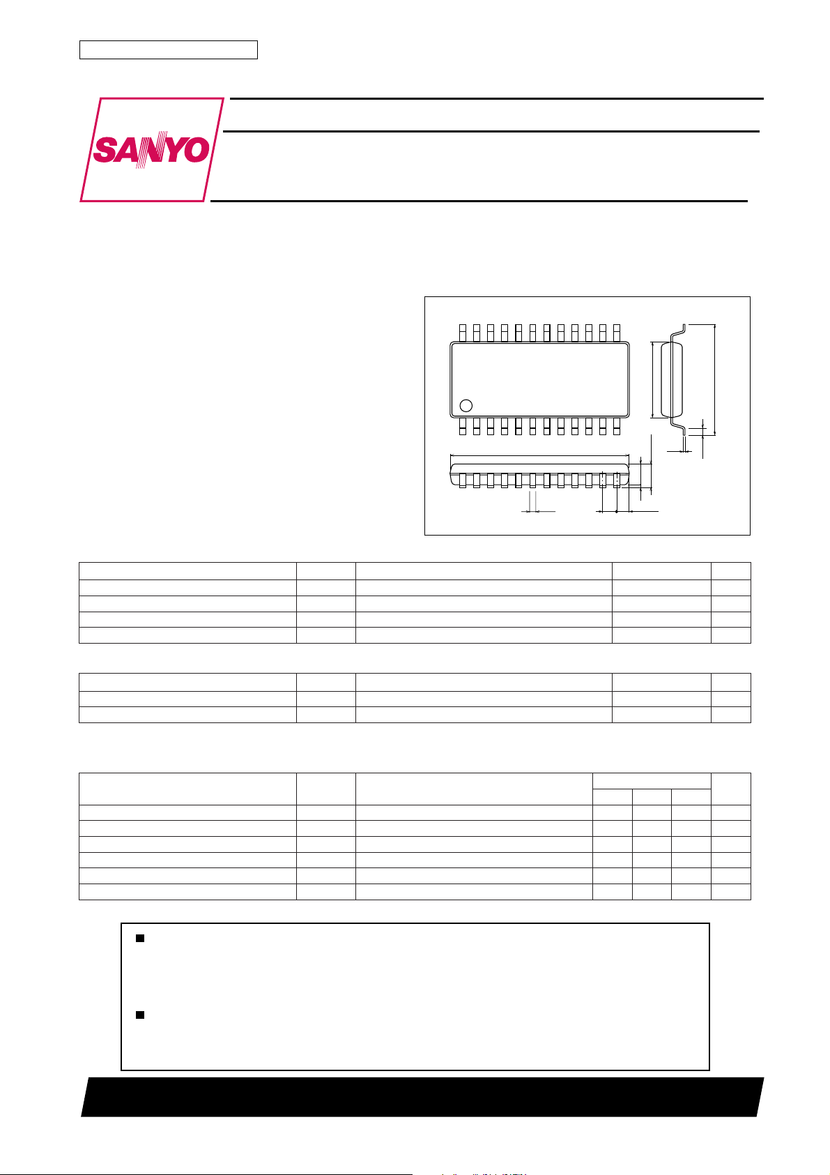
Package Dimensions
unit:mm
3112-MFP24S
24
112
[LA7155M]
12.5
0.35
13
5.4
0.15
1.7max
1.5
0.1
(0.75)
1.0
SANYO : MFP24S
7.6
0.63
˚C
˚C
Operating Conditions at Ta = 25˚C
retemaraPlobmySsnoitidnoCsgnitaRtinU
egatlovylppusdednemmoceRV
egnaregatlovgnitarepOV
* Both + and – voltages of supply are required.
CC
po 6±ot4±V
CC
Operating Characteristics at Ta = 25˚C, VCC=±5V and f=1kHz
retemaraPlobmySsnoitidnoC
niardtiucriCI
1egatlovtuptuOV
2egatlovtuptuOV
3egatlovtuptuOV
4egatlovtuptuOV
5egatlovtuptuOV
CC
1O
2VNIVBd6–=91–81–71–VBd
O
3VNIVBd6–=7–6–5–VBd
O
4VNIVBd8–=7–6–5–VBd
O
5VNIVBd81–=7–6–5–VBd
O
langisoN81141Am
V
VBd81–=91–81–71–VBd
NI
42000TN (KT)/41495HA/2142TS No.4064–1/5
sgnitaR
nimpytxam
Continued on next page.
5±V
tinU
Page 2
Continued from preceding page.
retemaraPlobmySsnoitidnoC
1noitrotsidcinomrahlatoTDHT
2noitrotsidcinomrahlatoTDHT
3noitrotsidcinomrahlatoTDHT
4noitrotsidcinomrahlatoTDHT
5noitrotsidcinomrahlatoTDHT
1egatlovtuptuomumixaMV
2egatlovtuptuomumixaMV
3egatlovtuptuomumixaMV
4egatlovtuptuomumixaMV
5egatlovtuptuomumixaMV
1egatlovesiontuptuOV
2egatlovesiontuptuOV
3egatlovesiontuptuOV
4egatlovesiontuptuOV
5egatlovesiontuptuOV
noitarapestupnIV
tesffoCDdehctiwSV
egatlovdlohedomHV
egatlovdlohedomLV
1
2
3
4
5
1MO
2MO
3MO
4MO
5MO
1NO
2NO
3NO
4NO
5NO
RC
CD
IHC
WOLC
LA7155M
nimpytxam
V
V
V
V
V
V
V3V,7V,01V,
V3V,7V,01V,
VBd81–=500.01.0%
NI
VBd6–=500.01.0%
NI
VBd6–=800.01.0%
NI
VBd8–=10.01.0%
NI
VBd81–=10.01.0%
NI
%1=DHT0.50.9VBd
%1=DHT7–3–VBd
%1=DHT0.60.9VBd
%1=DHT0.60.9VBd
%1=DHT0.60.9VBd
006=gR,langisoN Ω RETLIFOIDUANID,
NI
81
81
006=gR,tupnirehtO,VBd8–= Ω 08–Bd
langison42dna31sniptastuptuO02–002+Vm
5.3V+
00.1V
sgnitaR
011–401–VBd
011–401–VBd
701–101–VBd
501–99–VBd
101–49–VBd
CC
tinU
V
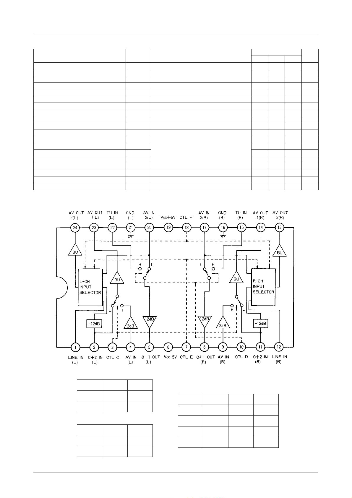
Block Diagram
AV OUT 1
lortnoC
3nip
L
H
C+1 OUT
lortnoC
01nip
L
H
tuptuO
HC-L
NI2+C
)L(
NIVA
)L(
tuptuO
HC-L
NIVA
)L(2
NIUT
)L(
tuptuO
HC-R
NI2+C
)R(
NIVA
)R(
tuptuO
HC-R
NIVA
)R(2
NIUT
)R(
AV OUT 2
lortnoC
7nip
LL
LH
HL
HH
lortnoC
81nip
tuptuO
HC-L
NIVA
)L(2
NIENIL
)L(
NI2+C
)L(
NIENIL
)L(
tuptuO
HC-R
NIVA
)R(2
NIENIL
)R(
NI2+C
)R(
NIENIL
)R(
No.4064–2/5
Page 3

Test Circuit
LA7155M
Pin Assignment
No.4064–3/5
Page 4

Table of switch operation
lobmyS1WS2WS3WS4WS5WS6WS7WS8WS9WS01WSCVDVEVFVtniopgnirusaeM
I
CC
V
L1-1O
V
R1-1O
V
L2-1O
V
R2-1O
V
L1-2O
V
R1-2O
V
L1-3O
V
R1-3O
V
L1-4O
V
R1-4O
V
L1-5O
V
R1-5O
V
L2-5O
V
R2-5O
DHT
L1-1
DHT
R1-1
DHT
L2-1
DHT
R2-1
DHT
L1-2
DHT
R1-2
DHT
L1-3
DHT
R1-3
DHT
L1-4
DHT
R1-4
DHT
L1-5
DHT
R1-5
DHT
L2-5
DHT
R2-5
V
L1-1MO
V
R1-1MO
V
L2-1MO
V
R2-1MO
V
L1-2MO
V
R1-2MO
V
L1-3MO
V
R1-3MO
V
L1-4MO
V
R1-4MO
V
L1-5MO
V
R1-5MO
V
L2-5MO
V
R2-5MO
V
L1-1NO
V
R1-1NO
V
L2-1NO
V
R2-1NO
V
L1-2NO
V
R1-2NO
V
L1-3NO
V
R1-3NO
V
L1-4NO
V
R1-4NO
V
L1-5NO
V
R1-5NO
V
L2-5NO
NOV
R2-5
2222222222LLLLA1A+2A+
1222222222LLLHV
2222212222LLLHV
2222122222LLLLV
2222222221LLLLV
2122222222LLHLV
2222221222LLHLV
2122222222LLHLV
2222221222LLHLV
2212222222HLHLV
2222222122HLHLV
2221222222HHHLV
2222222212HHHLV
2222122222HLHLV
2222222221HLHLV
1222222222LLLHV
2222212222LLLHV
2222122222LLLLV
2222222221LLLLV
2122222222LLHLV
2222221222LLHLV
2122222222LLHLV
2222221222LLHLV
2212222222HLHLV
2222222122HLHLV
2221222222HHHLV
2222222212HHHLV
2222122222HLHLV
2222222221HLHLV
1222222222LLLHV
2222212222LLLHV
2222122222LLLLV
2222222221LLLLV
2122222222LLHLV
2222221222LLHLV
2122222222LLHLV
2222221222LLHLV
2212222222HLHLV
2222222122HLHLV
2221222222HHHLV
2222222212HHHLV
2222122222HLHLV
2222222221HLHLV
2222222222LLLHV
2222222222LLLHV
2222222222LLLLV
2222222222LLLLV
2222222222LLHLV
2222222222LLHLV
2222222222LLHLV
2222222222LLHLV
2222222222HLHLV
2222222222HLHLV
2222222222HHHLV
2222222222HHHLV
2222222222HLHLV
2222222222HLHLV
LA7155M
3
1O
4O
1O
4O
1O
4O
2O
5O
2O
5O
3O
6O
3O
6O
1O
4O
1O
4O
1O
4O
2O
5O
2O
5O
3O
6O
3O
6O
1O
4O
1O
4O
1O
4O
2O
5O
2O
5O
3O
6O
3O
6O
1O
4O
1O
4O
1O
4O
2O
5O
2O
5O
3O
6O
3O
6O
Continued on next page.
No.4064–4/5
Page 5

Continued from preceding page.
lobmyS1WS2WS3WS4WS5WS6WS7WS8WS9WS01WSCVDVEVFVtniopgnirusaeM
V
L1-RC
V
R1-RC
V
L2-RC
V
R2-RC
V
L3-RC
V
R3-RC
V
L4-RC
V
R4-RC
V
L5-RC
V
R5-RC
V
L6-RC
V
R6-RC
V
L7-RC
V
R7-RC
V
L-CD
V
R-CD
V
3-1HC
V
7-1HC
V
01-1HC
V
81-1HC
V
3-WOLC
V
7-WOLC
V
V
01-WOLC
81-WOLC
1222222222LLLHV
2222212222LLLHV
2222122222LLLLV
2222222221LLLLV
2122222222LLHLV
2222221222LLHLV
2122222222LLHLV
2222221222LLHLV
2212222222HLHLV
2222222122HLHLV
2221222222HHHLV
2222222212HHHLV
2222122222HLHLV
2222222221HLHLV
2222222222LLH/LH/LV
2222222222LLH/LH/LV
2212222222–LHLV
2122222222LL–LV
2221222222H–HLV
1222222222LLL–V
2122222222–LHLV
2222122222LL–LV
2222122222H–HLV
2222122222LLL–V
LA7155M
6,5,4,3,2O
6,5,3,2,1O
6,5,4,3,2O
6,5,3,2,1O
6,5,4,3,2O
6,5,3,2,1O
6,5,4,3,1O
6,4,3,2,1O
6,5,4,3,1O
6,4,3,2,1O
6,5,4,2,1O
5,4,3,2,1O
6,5,4,2,1O
5,4,3,2,1O
1O
4O
C
F
D
E
C
F
D
E
Specifications of any and all SANYO products described or contained herein stipulate the performance,
characteristics, and functions of the described products in the independent state, and are not guarantees
of the performance, characteristics, and functions of the described products as mounted in the customer's
products or equipment. To verify symptoms and states that cannot be evaluated in an independent device,
the customer should always evaluate and test devices mounted in the customer's products or equipment.
SANYO Electric Co., Ltd. strives to supply high-quality high-reliability products. However, any and all
semiconductor products fail with some probability. It is possible that these probabilistic failures could
give rise to accidents or events that could endanger human lives, that could give rise to smoke or fire,
or that could cause damage to other property. When designing equipment, adopt safety measures so
that these kinds of accidents or events cannot occur. Such measures include but are not limited to protective
circuits and error prevention circuits for safe design, redundant design, and structural design.
In the event that any or all SANYO products(including technical data,services) described or
contained herein are controlled under any of applicable local export control laws and regulations,
such products must not be exported without obtaining the export license from the authorities
concerned in accordance with the above law.
No part of this publication may be reproduced or transmitted in any form or by any means, electronic or
mechanical, including photocopying and recording, or any information storage or retrieval system,
or otherwise, without the prior written permission of SANYO Electric Co. , Ltd.
Any and all information described or contained herein are subject to change without notice due to
product/technology improvement, etc. When designing equipment, refer to the "Delivery Specification"
for the SANYO product that you intend to use.
Information (including circuit diagrams and circuit parameters) herein is for example only ; it is not
guaranteed for volume production. SANYO believes information herein is accurate and reliable, but
no guarantees are made or implied regarding its use or any infringements of intellectual property rights
or other rights of third parties.
This catalog provides information as of April, 2000. Specifications and information herein are subject to
change without notice.
PS No.4064–5/5
 Loading...