

Page 1
Any and all SANYO products described or contained herein do not have specifications that can handle
applications that require extremely high levels of reliability, such as life-support systems, aircraft’s
control systems, or other applications whose failure can be reasonably expected to result in serious
physical and/or material damage. Consult with your SANYO representative nearest you before using
any SANYO products described or contained herein in such applications.
SANYO assumes no responsibility for equipment failures that result from using products at values that
exceed, even momentarily, rated values (such as maximum ratings, operating condition ranges,or other
parameters) listed in products specifications of any and all SANYO products described or contained
herein.
Monolithic Linear IC
Audio / Video Switch
for VCR Video Camera Use
Ordering number:ENN4020A
LA7151, 7151M
SANYO Electric Co.,Ltd. Semiconductor Company
TOKYO OFFICE Tokyo Bldg., 1-10, 1 Chome, Ueno, Taito-ku, TOKYO, 110-8534 JAPAN
Overview
The LA7151 and LA7151M are high-performance, dualchannel audio/video switches designed for video camera
applications.
The LA7151 and LA7151M have a wide bandwidth, low
supply current and a large dynamic range, making them
ideal for low-power or battery operated equipment.
The LA7151 and LA7151M operate from a 4.5 to 12.5V
supply and are available in 12-pin SIPs and 10-pin MFPs,
respectively.
Features
• Two, separately controllable switch circuits.
• 50kΩ input impedance.
• Low supply current.
• Large dynamic range.
• Wide bandwidth.
• 4.5 to 12.5V supply voltage.
• 12-pin SIP (LA7151) and 10-pin MFP (LA7151M).
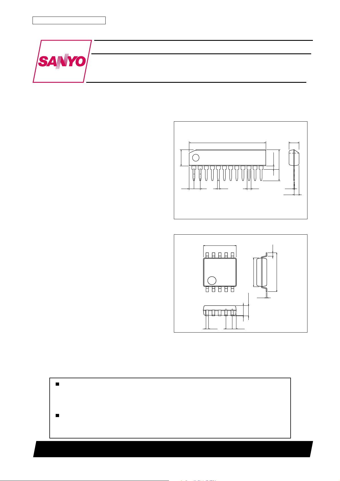
Package Dimensions
unit:mm
3116-SIP12S
[LA7151]
22.3
4.8
1
1.36
unit:mm
3086B-MFP10S
1.78
0.5
[LA7151M]
5.0
10
6
12
1.1
3.0
5.7max
0.51min
3.2
0.25
1.475
SANYO : SIP12S
0.63
1
5
1.7max
(1.5)˚
0.1
(0.5)
1.00.35
O2500TN (KT)/2182/D161TS No.4020–1/5
4.4
0.15
SANYO : MFP10S
6.4
Page 2
LA7151, 7151M
Specifications
Maximum Ratings at Ta = 25˚C
retemaraPlobmySsnoitidnoCsgnitaRtinU
egatlovylppusmumuxaMV
noitapissidrewopelbawollAxamdP 051Wm
erutarepmetgnitarepOrpoT 08+ot02–
erutarepmetegarotSgtsT 051+ot55–
Recommended Operating Conditions at Ta = 25˚C
retemaraPlobmySsnoitidnoCsgnitaRtinU
egatlovylppuSV
egnaregatlovylppuSV
Operating Characteristics at Ta = 25˚C, VCC=5V
retemaraPlobmySsnoitidnoC
niardtnerruCI
noitrotsidcinomrahlatoTDHTV
egatlovtuptuomumixaMV
egatlovesiontuptuOV
sehctiwsneewtebklatssorCTC
slennahcneewtebklatssorCTC
noitrotsidcinomrah-dnoceS2HV
noitrotsidcinomrah-drihT3HV
citsiretcarahcycneuqerFfGzHM01/zHk001=f,p-pV2=NIV1–01+Bd
niagegatloVGVV
tesffoCDtuptuOfoV
egatlovnoitnetertupniAhctiwSV
egatlovnoitnetertupniBhctiwSV
ecnadepmitupnIZ
ecnadepmituptuOZ
xam 51V
CC
Ta≤80˚C
CC
po 5.21ot5.4V
CC
CC
NI
MO
NO
S
C
AC
BC
NI
TUO
006=gR Ω retlifOIDUANID,011–001–Bd
05=gR Ω V,
05=gR Ω V,
NI
NI
NI
sgnitaR
nimpytxam
V,tupnioN
V5=5.50.75.8Am
CC
V,tupnioN
V9=0.65.70.9Am
CC
V,tupnioN
V21=5.60.85.9Am
CC
zHk1=f,p-pV1=600.01.0%
%1=DHT,zHk1=f2.25.2p-pV
NI
NI
BdnaAsehctiwsneewteb
2dna1slennahcneewteb
zHM34.4=f,p-pV2=05–04–Bd
zHM34.4=f,p-pV2=55–54–Bd
zHM34.4=f,p-pV2=3.0–03.0+Bd
BdnaAsehctiws
2LTC,1LTC:CD5.30.5V
2LTC,1LTC:CD05.1V
derusaem,zHM34.4=f,p-pV2=
derusaem,zHM34.4=f,p-pV2=
neewtebgnihctiwsnehwecnereffidegatlovtuptuO
06–55–Bd
56–06–Bd
03–003+Vm
05kΩ
01
˚C
˚C
21,9,5V
tinU
Ω
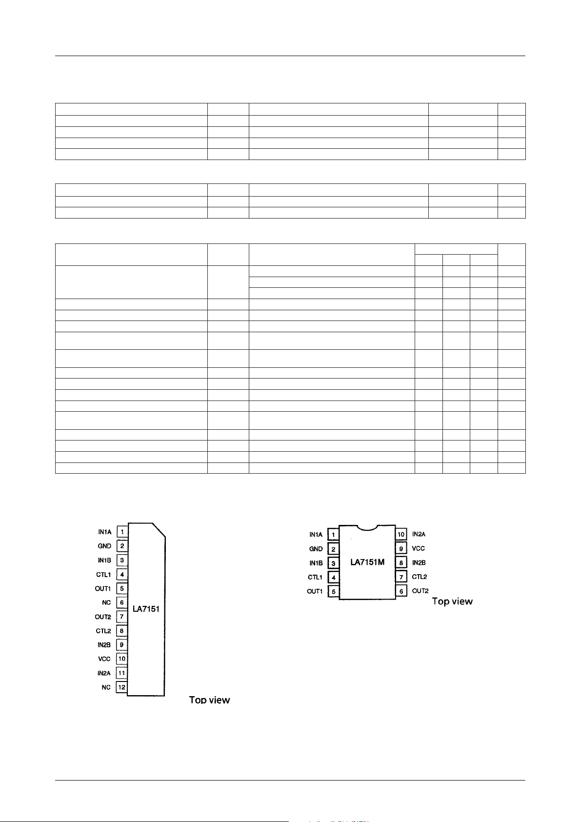
Pin Assignments
LA7151 LA7151M
No.4020–2/5
Page 3

Block Diagram
LA7151
LA7151, 7151M
LA7151M
1
IN1A
23
IN2A
10
A
B
IN1B
9
V
CC
B
A
A
B
CH-1
4
CTL15OUT1
IN2B
8
CH-2
CH-1
7
6
OUT28CTL29IN2B
N.C.
CTL2
7
CH-2
OUT2
A
B
V
CC
10
11
12
IN2A
N.C.
A13256
LTC
HAA
LBB
1HC2HC
6
Test Circuit
LA7151
1
IN1A
2
3
IN1B
4
CTL1
5
OUT1
LTC
HAA
LBB
LA7151
123456789101112
+
10µF
S1
BA
+
RG
S2
RG
+
BA
+
10µF
S3
BA
0.01µF
47µF
A
+
S6
BA
+
+
10µF
+
10µF
S4
BA
10kΩ
10kΩ
+
10µF
S5
BA
+
RG
CTL
RG
V
CC
+
+
47µF
0.01µF
1HC2HC
A13257
10µF
A13258
No.4020–3/5
Page 4

LA7151M
LA7151, 7151M
Pin Functions
.oNniP
PISPFM
11 A1NI
RG
+
BA
S6
+
10 9 8 7 6
+
47µF
0.01µF
12345
+
S1
BA
+
RG
emaNniPtiucrictnelaviuqE
10µF
10µF
RG
V
CC
A
LA7151M
RG
Input pin
BA
S5
+
+
S2
BA
+
+
10µF
10µF
V
AB
AB
CC
CTL
10kΩ
+
10µF
S4
0.01µF
+
47µF
S3
+
10µF
10kΩ
A13259
egatlovCD
V(
)V5
CC
noitpircseD
33 B1NI
500Ω 50kΩ
98 B2NI
200µA
1101A2NI
22 DNG V0
44 1LTC
1kΩ 1kΩ
50µA
15kΩ
A13260
CTL pin
65kΩ
87 2LTC
55 1TUO
100µA
A13261
V
CC
Output pin
V
V01.3
V83.2
CC
VCCV21V97.7:
V
CC
VCCV21V70.7:
V87.5:V9
V60.5:V9
76 2TUO
621–
–
019V
CC
1mA
A13262
.C.N DNGroNEPO
V0.5
No.4020–4/5
Page 5

LA7151, 7151M
Specifications of any and all SANYO products described or contained herein stipulate the performance,
characteristics, and functions of the described products in the independent state, and are not guarantees
of the performance, characteristics, and functions of the described products as mounted in the customer's
products or equipment. To verify symptoms and states that cannot be evaluated in an independent device,
the customer should always evaluate and test devices mounted in the customer's products or equipment.
SANYO Electric Co., Ltd. strives to supply high-quality high-reliability products. However, any and all
semiconductor products fail with some probability. It is possible that these probabilistic failures could
give rise to accidents or events that could endanger human lives, that could give rise to smoke or fire,
or that could cause damage to other property. When designing equipment, adopt safety measures so
that these kinds of accidents or events cannot occur. Such measures include but are not limited to protective
circuits and error prevention circuits for safe design, redundant design, and structural design.
In the event that any or all SANYO products(including technical data,services) described or
contained herein are controlled under any of applicable local export control laws and regulations,
such products must not be exported without obtaining the export license from the authorities
concerned in accordance with the above law.
No part of this publication may be reproduced or transmitted in any form or by any means, electronic or
mechanical, including photocopying and recording, or any information storage or retrieval system,
or otherwise, without the prior written permission of SANYO Electric Co. , Ltd.
Any and all information described or contained herein are subject to change without notice due to
product/technology improvement, etc. When designing equipment, refer to the "Delivery Specification"
for the SANYO product that you intend to use.
Information (including circuit diagrams and circuit parameters) herein is for example only ; it is not
guaranteed for volume production. SANYO believes information herein is accurate and reliable, but
no guarantees are made or implied regarding its use or any infringements of intellectual property rights
or other rights of third parties.
This catalog provides information as of October, 2000. Specifications and information herein are subject
to change without notice.
PS No.4020–5/5
 Loading...