

Page 1
Any and all SANYO products described or contained herein do not have specifications that can handle
applications that require extremely high levels of reliability, such as life-support systems, aircraft’s
control systems, or other applications whose failure can be reasonably expected to result in serious
physical and/or material damage. Consult with your SANYO representative nearest you before using
any SANYO products described or contained herein in such applications.
SANYO assumes no responsibility for equipment failures that result from using products at values that
exceed, even momentarily, rated values (such as maximum ratings, operating condition ranges,or other
parameters) listed in products specifications of any and all SANYO products described or contained
herein.
Monolithic Linear IC
2-Channel BTL-Use or 4-Channel Driver
Ordering number:ENN3266
LA6533
SANYO Electric Co.,Ltd. Semiconductor Company
TOKYO OFFICE Tokyo Bldg., 1-10, 1 Chome, Ueno, Taito-ku, TOKYO, 110-8534 JAPAN
Overview
The LA6533 is a 2-channel BTL-use driver
designed for compact disc pickup actuation
or a 4-channel driver for general-purpose
applications.
Functions and Features
• High output current (IO max=0.5A).
• Wide operating voltage range (4 to 15V).
• Low input bias current.
• On-chip thermal shutdown.
• Output of amps 1 to 4 at muting-ON.
mode:OFF.
Specifications
Maximum Ratings at Ta = 25˚C
retemaraPlobmySsnoitidnoCsgnitaRtinU
egatlovylppusmumixaMV
noitapissidrewopelbawollAxamdP 9.1W
egatlovtupnimumixaMV
tnerrucnipgnituMI
tnerructuptuomumixaMI
erutarepmetgnitarepOrpoT 57+ot02–
erutarepmetegarotSgtsT 051+ot55–
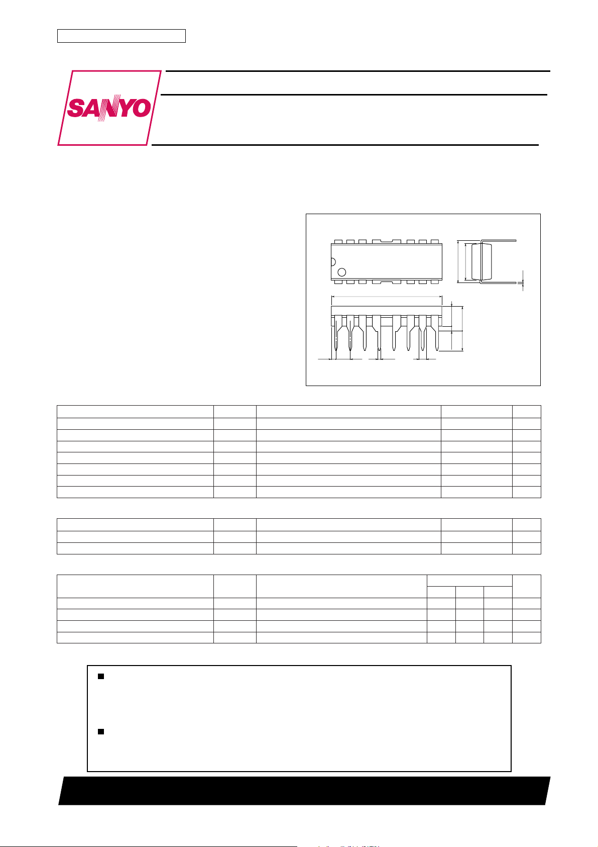
Package Dimensions
unit:mm
3054A-DIP16F
[LA6533]
16
1
0.81 2.54
xam 61V
CC
xamreifilpmareffuB 51V
BNI
xam 1Am
M
xam 7.0A
O
19.4
0.5
9
6.45
7.62
8
3.46
4.26max
3.5
0.51min
1.3
SANYO : DIP16F
0.4
˚C
˚C
Operating Conditions at Ta = 25˚C
retemaraPlobmySsnoitidnoCsgnitaRtinU
egatlovylppusmumixaMV
ecnatsiserdaoLR
CC
L
41ot11,6ot3sniP 8
Operating Characteristics at Ta = 25˚C, VCC=5.0V
retemaraPlobmySsnoitidnoC
1niardtnerrucdedaol-oNI
2niardtnerrucdedaol-oNI
3niardtnerrucdedaol-oNI
4niardtnerrucdedaol-oNI
11etoN,FFOetuM50102Am
CC
2NOetuM 3751Am
CC
32etoN,FFOetuM010203Am
CC
4NOetuM 4861Am
CC
40500TN (KOTO)/N019TA, TS No.3266–1/4
sgnitaR
nimpytxam
Continued on next page.
5V
Ω
tinU
Page 2
Continued from preceding page.
retemaraPlobmySsnoitidnoC
1egatlovtesffotuptuOV
2egatlovtesffotuptuOV
ecnereffidegatlovtuptuo-tupnireffuBV
egnaregatlovtupnireffuBV
egnaregatlovtupnipmAV
tnerrucsaibtupnII
egatlovtuptuOV
ecnereffidegatlovtuptuoegdirBV
niagegatlovtiucric-desolCV
egatlovetats-nonipgnituMV
tnerrucni-wolfnipgnituMI
Note 1) Pins 2, 7, 10, 15 : GND
Note 2) Pins 2, 7, 10, 15 : 1/2V
CC
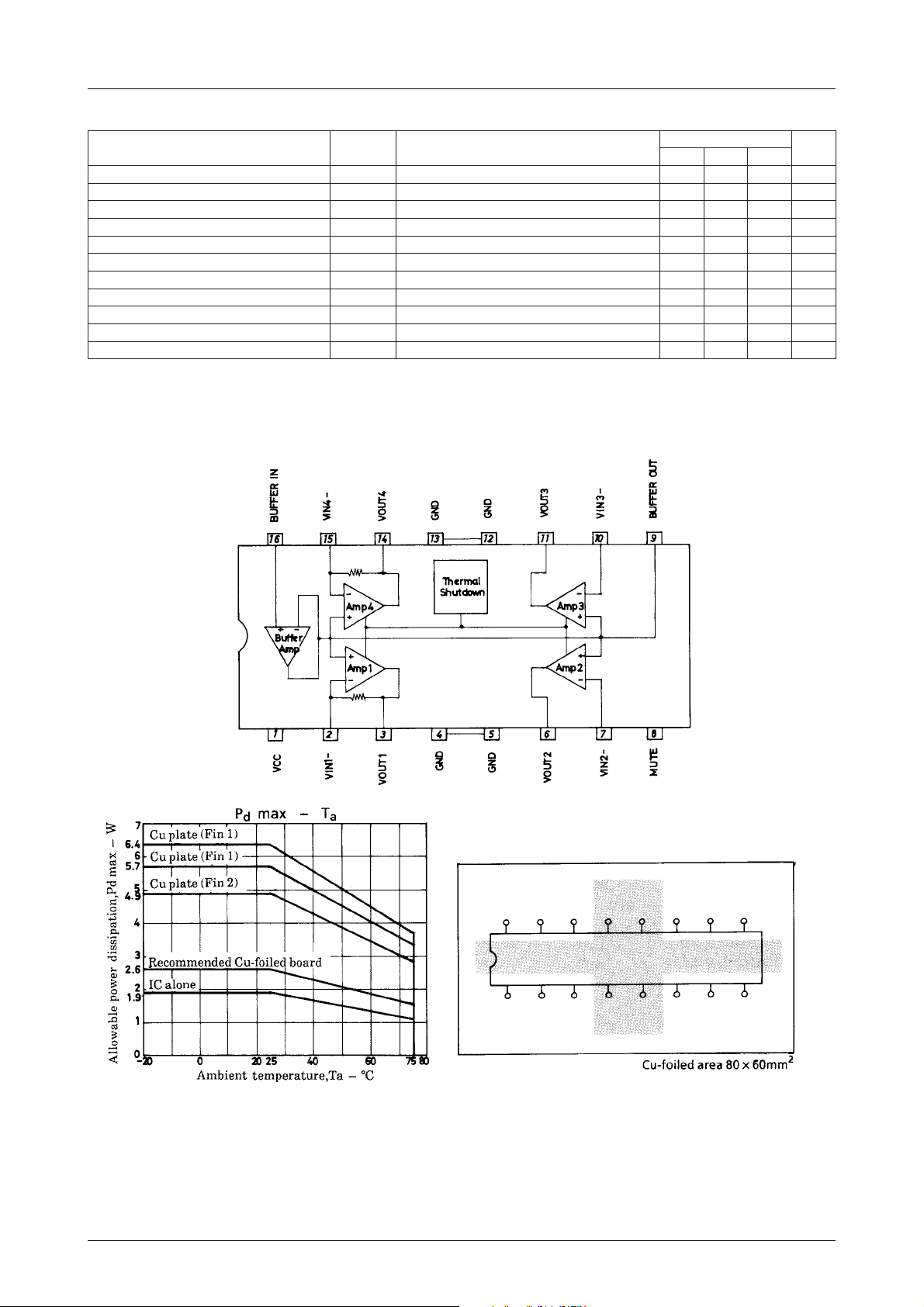
Equivalent Circuit Block Diagram
LA6533
sgnitaR
nimpytxam
12tuOdna1tuO05–05+Vm
FO
24tuOdna3tuO05–05+Vm
FO
OIB
MCIB
MCI
B
RL0.8= Ω 8.23.3V
O
8Ω .41dna11,6dna3snipneewtebdaol8.12.2V
DO
G
M
M
reifilpmareffuB03–03+Vm
reifilpmareffuB5.1
0.1
VCC5.1–
VCC5.1–
05An
0.6Bd
7.0V
0.3Aµ
tinU
V
V
Sample Printed Circuit Pattern
No.3266–2/4
Page 3

Sample Application Circuit
LA6533
No.3266–3/4
Page 4

LA6533
Specifications of any and all SANYO products described or contained herein stipulate the performance,
characteristics, and functions of the described products in the independent state, and are not guarantees
of the performance, characteristics, and functions of the described products as mounted in the customer's
products or equipment. To verify symptoms and states that cannot be evaluated in an independent device,
the customer should always evaluate and test devices mounted in the customer's products or equipment.
SANYO Electric Co., Ltd. strives to supply high-quality high-reliability products. However, any and all
semiconductor products fail with some probability. It is possible that these probabilistic failures could
give rise to accidents or events that could endanger human lives, that could give rise to smoke or fire,
or that could cause damage to other property. When designing equipment, adopt safety measures so
that these kinds of accidents or events cannot occur. Such measures include but are not limited to protective
circuits and error prevention circuits for safe design, redundant design, and structural design.
In the event that any or all SANYO products(including technical data,services) described or
contained herein are controlled under any of applicable local export control laws and regulations,
such products must not be exported without obtaining the export license from the authorities
concerned in accordance with the above law.
No part of this publication may be reproduced or transmitted in any form or by any means, electronic or
mechanical, including photocopying and recording, or any information storage or retrieval system,
or otherwise, without the prior written permission of SANYO Electric Co. , Ltd.
Any and all information described or contained herein are subject to change without notice due to
product/technology improvement, etc. When designing equipment, refer to the "Delivery Specification"
for the SANYO product that you intend to use.
Information (including circuit diagrams and circuit parameters) herein is for example only ; it is not
guaranteed for volume production. SANYO believes information herein is accurate and reliable, but
no guarantees are made or implied regarding its use or any infringements of intellectual property rights
or other rights of third parties.
This catalog provides information as of April, 2000. Specifications and information herein are subject to
change without notice.
PS No.3266–4/4
 Loading...