

Page 1
Any and all SANYO products described or contained herein do not have specifications that can handle
applications that require extremely high levels of reliability, such as life-support systems, aircraft’s
control systems, or other applications whose failure can be reasonably expected to result in serious
physical and/or material damage. Consult with your SANYO representative nearest you before using
any SANYO products described or contained herein in such applications.
SANYO assumes no responsibility for equipment failures that result from using products at values that
exceed, even momentarily, rated values (such as maximum ratings, operating condition ranges,or other
parameters) listed in products specifications of any and all SANYO products described or contained
herein.
Monolithic Linear IC
0.5A Power Operational Amplifier
Ordering number:ENN2612A
LA6515
SANYO Electric Co.,Ltd. Semiconductor Company
TOKYO OFFICE Tokyo Bldg., 1-10, 1 Chome, Ueno, Taito-ku, TOKYO, 110-8534 JAPAN
Overview
The LA6515 is a high-performance power operational amplifier IC capable of delivering larger output currents than
conventional operational amplifiers.
The LA6515 features an on-chip current limiter and provides high voltage gain and a high common-mode rejection ratio.
The LA6515 is an ideal choice for power applications such
as DC servos, capstan drivers, actuator drivers, programmable power supplies and high-quality audio amplifiers.
The LA6515 is available in 10-pin SIPs and operates from
–15V and 15V supplies.
Features
• 0.5A output current.
• 100dB voltage gain.
• 80dB common-mode rejection.
• 0.15 V/µs slew rate.
• 2mV offset voltage.
• 10nA offset current.
• On-chip current limiter.
• –15V and 15V supplies.
• 10-pin SIP.
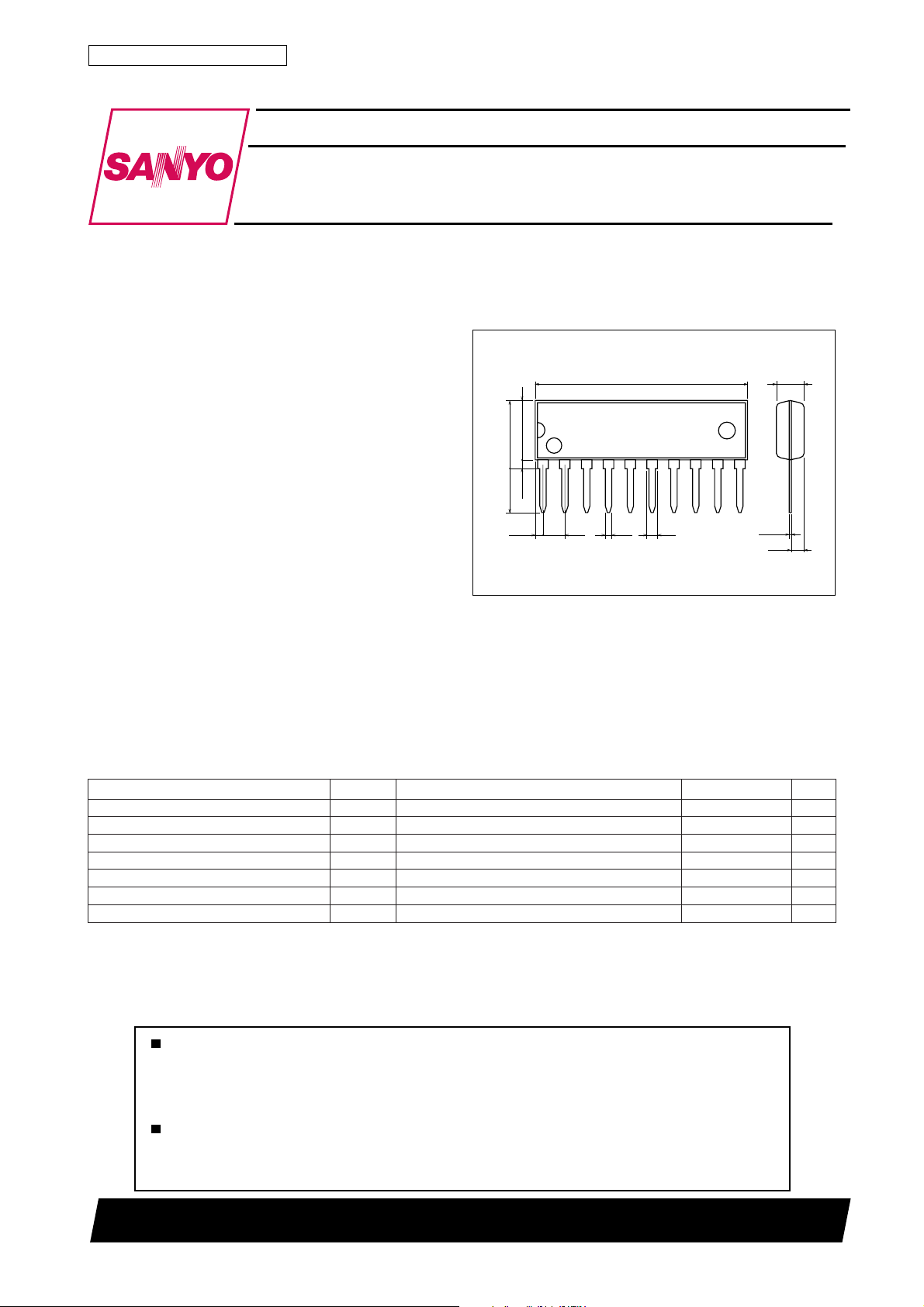
Package Dimensions
unit:mm
3043A-SIP10
[LA6515]
24.2
6.5
7.7max
4.9
1.1min
1
0.5
3.25
10
1.22.540.67
0.25
1.5
SANYO : SIP10
Specifications
Maximum Ratings at Ta = 25˚C
retemaraPlobmySsnoitidnoCsgnitaRtinU
egatlovylppuSV
egatlovtupnilaitnereffiDV
egatlovtupniedom-nommoCV
tnerructuptuOI
noitapissidrewopelbawollAxamdP 3.1W
erutarepmetgnitarepOrpoT 57+ot02–
erutarepmetegarotSgtsT 051+ot55–
CCV/EE
DI
MCI
xam 0.1A
O
40500TN (KT)/D250JK No.2612–1/3
81±V
03V
51±V
˚C
˚C
Page 2
LA6515
Electrical Characteristics at Ta = 25˚C, VCC/VEE=±15V
retemaraPlobmySsnoitidnoC
tnerructnecseiuQI
egatlovtesffotupnIV
tnerructesffotupnII
tnerrucsaibtupnII
egnaregatlovtupniedom-nommoCV
noitcejeredom-nommoCRMC0708Bd
egatlovtuptuomumixaMV
niagegatloVGV
etarwelSRSR,0=VG
egatlovesiontupnitnelaviuqEV
oitarnoitcejeregatlovylppuSRRVS 03051V/Vµ
tnerrucgnitimiLI
OCC
RS≤ k01 Ω 26Vm
OI
OI
B
MCI
RL33= Ω 21±31±V
O
O
L
IN
CS
k1=gR Ω OIDUANID,2Vµ
RCS2.2= Ω 53.0A
sgnitaR
nimpytxam
62102Am
01002An
001007An
51–31+V
001Bd
33= Ω 2.2=R, Ω Fµ1.0=L,51.0sµ/V
tinU
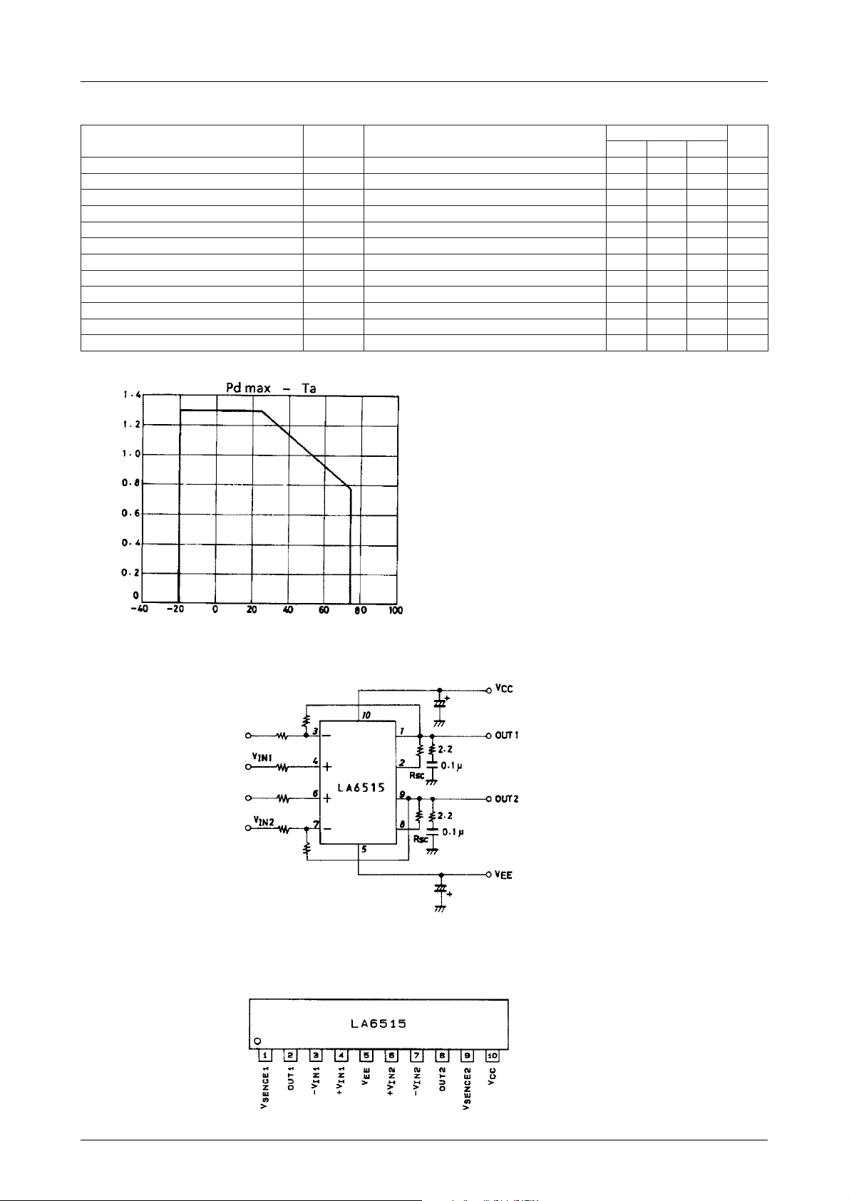
Allowable power dissipation, Pd max – W
Ambient temperature, Ta – °C
Sample Application Circuit
Pin Assignment
No.2612–2/3
Page 3

LA6515
Specifications of any and all SANYO products described or contained herein stipulate the performance,
characteristics, and functions of the described products in the independent state, and are not guarantees
of the performance, characteristics, and functions of the described products as mounted in the customer's
products or equipment. To verify symptoms and states that cannot be evaluated in an independent device,
the customer should always evaluate and test devices mounted in the customer's products or equipment.
SANYO Electric Co., Ltd. strives to supply high-quality high-reliability products. However, any and all
semiconductor products fail with some probability. It is possible that these probabilistic failures could
give rise to accidents or events that could endanger human lives, that could give rise to smoke or fire,
or that could cause damage to other property. When designing equipment, adopt safety measures so
that these kinds of accidents or events cannot occur. Such measures include but are not limited to protective
circuits and error prevention circuits for safe design, redundant design, and structural design.
In the event that any or all SANYO products(including technical data,services) described or
contained herein are controlled under any of applicable local export control laws and regulations,
such products must not be exported without obtaining the export license from the authorities
concerned in accordance with the above law.
No part of this publication may be reproduced or transmitted in any form or by any means, electronic or
mechanical, including photocopying and recording, or any information storage or retrieval system,
or otherwise, without the prior written permission of SANYO Electric Co. , Ltd.
Any and all information described or contained herein are subject to change without notice due to
product/technology improvement, etc. When designing equipment, refer to the "Delivery Specification"
for the SANYO product that you intend to use.
Information (including circuit diagrams and circuit parameters) herein is for example only ; it is not
guaranteed for volume production. SANYO believes information herein is accurate and reliable, but
no guarantees are made or implied regarding its use or any infringements of intellectual property rights
or other rights of third parties.
This catalog provides information as of April, 2000. Specifications and information herein are subject to
change without notice.
PS No.2612–3/3
 Loading...