

SANYO LA5616 Datasheet
Overview
The LA5616 is appropriate for use in power supplies for
microprocessor-controlled CD players, tuners, receivers,
and similar audio equipment.
Functions
• Low-saturation 5-V, 400-mA power supply
• 7.0-V, 1.0-A power supply
• Output reset generation function
• The 5.0-V system can be controlled (on/off) from the
provided active-high enable pin.
Features
• The reset output delay time can be set with an external
capacitor.
• Sharp-cutoff current limiter circuit and thermal
protection circuit
• Active pull-up element incorporated in reset output
circuit for improved noise suppression.
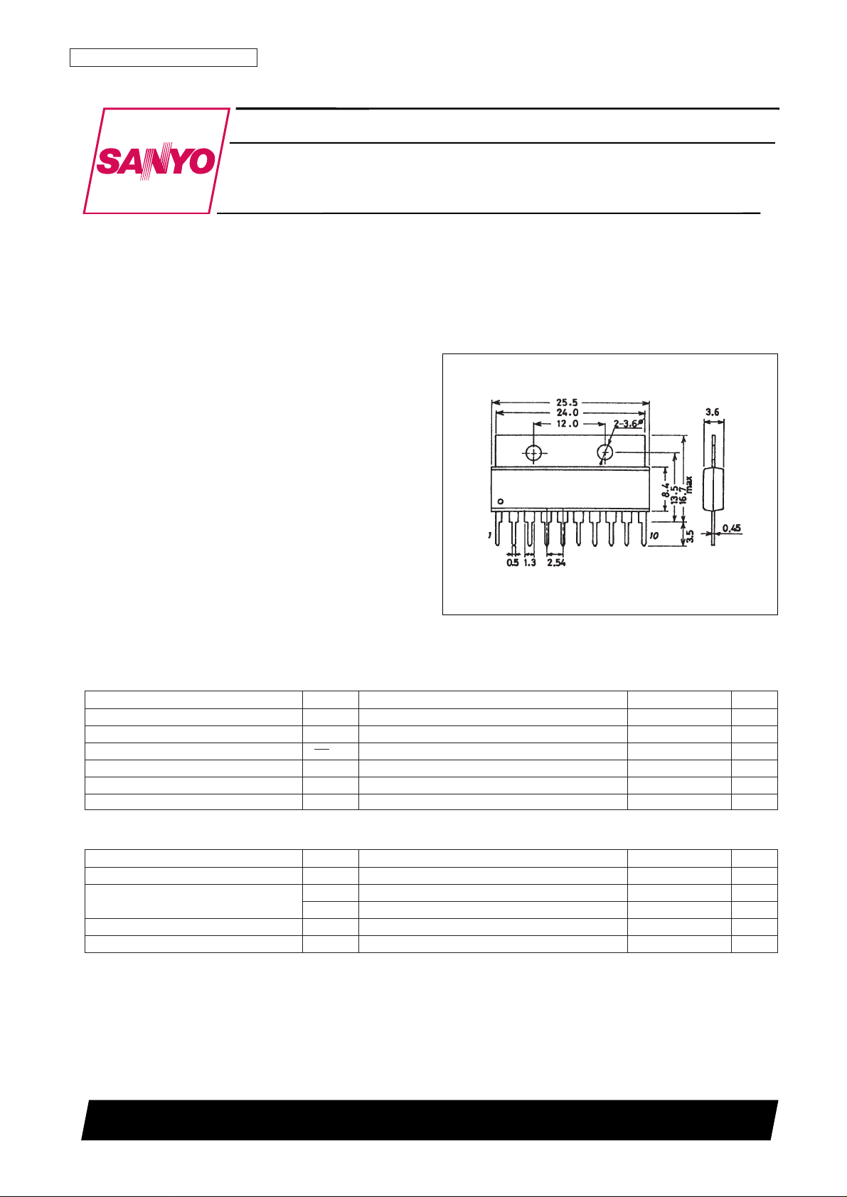
Package Dimensions
unit: mm
3018A-SIP10F
Monolithic Linear IC
93096HA (OT)No. 5286-1/5
SANYO: SIP10F
[LA5616]
SANYO Electric Co.,Ltd. Semiconductor Bussiness Headquarters
TOKYO OFFICE Tokyo Bldg., 1-10, 1 Chome, Ueno, Taito-ku, TOKYO, 110 JAPAN
Microprocessor-Controlled
Audio Power Supply
LA5616
Ordering number : EN5286
Specifications
Absolute Maximum Ratings at Ta = 25°C
Parameter Symbol Conditions Ratings Unit
Input voltage V
IN
max 18 V
Enable pin voltage V
EN
max VINmax V
Reset output pin voltage V
RES
max 18 V
Allowable power dissipation Pd max 2W
Operating temperature Topr –20 to +80 °C
Storage temperature Tstg –55 to +150 °C
Operating Conditions at Ta = 25°C
Parameter Symbol Conditions Ratings Unit
Input voltage V
IN
5.6 to 17 V
Output current
I
OUT
1 0 to 400 mA
I
OUT
2 0 to 1.0 A
Reset output source current I
ORH
High level 0 to 200 µA
Reset output sink current I
ORL
Low level 0 to 2 mA

No. 5286-2/5
LA5616
Parameter Symbol Conditions
Ratings
Unit
min typ max
[5.0-V Power Supply Block] V
IN
1 = VIN2, C
OUT
2 = 47 µF
Output voltage V
OUT
1 VIN1 = 12 V, I
OUT
1 = 400 mA 4.75 5.0 5.25 V
Dropout voltage V
DROP
1 VIN1 = 4.9 V, I
OUT
1 = 400 mA 0.5 1.0 V
Line regulation ∆V
OLN
1 5.6 ≤ VIN1 ≤ 17 V, I
OUT
1 = 400 mA 20 100 mV
Load regulation ∆V
OLD
1 5 mA ≤ IO≤ 400 mA, VIN1 = 12 V 50 150 mV
Peak output current I
OP
1 VIN1 = 12 V 400 500 mA
Output shorted current I
OSC
1 VIN1 = 12 V 100 400 mA
Output noise voltage V
N
1 10 Hz ≤ f ≤ 100 kHz 70 µVrms
Output voltage temperature
∆V
O
/∆Tal Tj = 25 to 125°C 1.6 mV/°C
coefficient
Ripple rejection Rref1 f = 120 Hz, 6 V ≤V
IN
1 ≤ 17 V 60 dB
Output on control voltage V
ENH
1 VIN1 = 12 V 2.6 V
Output off control voltage V
ENL
1 VIN1 = 12 V 1.0 V
Low-level output voltage V
O OFF
1 VIN1 = 12 V 0.3 V
[Reset Block] V
IN
1 = VIN2 = 12 V
High reset output voltage V
ORHIORH
= 200 µA, Cd pin open 4.73 4.98 5.23 V
Low reset output voltage V
ORLISRL
= 2 mA, with Cd shorted to GND 100 200 mV
Reset threshold voltage V
RT
3.95 4.2 4.45 V
Reset hysteresis voltage Vhys 40 100 200 mV
Reset output delay time td Cd = 0.1 µF 7.5 10 12.5 ms
[7.0-V Power Supply Block] V
IN
1 = VIN2, C
OUT
2 = 47 µF
Output voltage V
OUT
2 VIN2 = 12 V, I
OUT
2 = 1 A 6.5 7.0 7.5 V
Dropout voltage V
DROP
2 VIN2 = 6.5 V, I
OUT
2 = 1 A 1.0 2.0 V
Line regulation ∆V
OLN
2 9.0 ≤ VIN2 ≤ 17 V, I
OUT
2 = 1 A 200 mV
Load regulation ∆V
OLD
2 5 mA ≤ IO≤ 1.0 A, VIN2 = 12 V 300 mV
Peak output current I
OP
2 VIN2 = 12 V 1.0 A
Output shorted current I
OSC
2 VIN2 = 12 V 500 mA
Ripple rejection Rref2 f = 120 Hz, 9.0 V ≤ V
IN
2 ≤ 17 V 50 dB
Output on control voltage V
ENH
2 VIN2 = 12 V 2.6 V
Output off control voltage V
ENL
2 VIN2 = 12 V 1.0 V
Low-level output voltage V
O OFF
2 VIN2 = 12 V 0.3 V
Electrical Characteristics at Ta = 25°C
 Loading...