

SANYO LA5613 Datasheet
Parameter Symbol Conditions Ratings Unit
Maximum supply voltage
V
CC
1 max 14
V
V
CC
2 max VCC1 ≥ VCC2V
CC
1
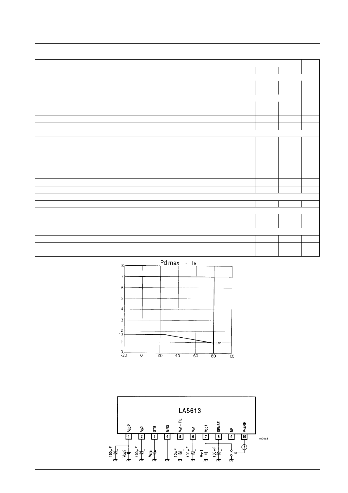
Allowable power dissipation Pd max No heat sink 1.7 W
Operating temperature Topr –20 to +80 °C
Storage temperature Tstg –40 to +150 °C
Ordering number : EN5669
53197HA(OT) No. 5669-1/4
Overview
The LA5613 is an IC that includes an independently
on/off switchable 5-V/0.7-A low-saturation regulator, an
11.3-V/0.3-A ripple filter, and a control amplifier on chip.
It is optimal for use in VCR and similar products.
Functions and Features
• 5-V/0.7-A low-saturation regulator
(Includes an on/off function.)
• 11.3-V/0.3-A ripple filter (Includes an on/off function.)
• Switching regulator control amplifier
• Includes input overvoltage and thermal protection
circuits on chip.
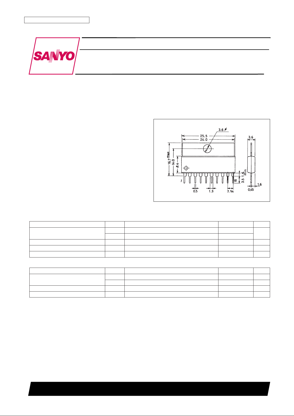
Package Dimensions
unit: mm
3046B-SIP10F
SANYO: SIP10H
[LA5613]
LA5613
SANYO Electric Co.,Ltd. Semiconductor Bussiness Headquarters
TOKYO OFFICE Tokyo Bldg., 1-10, 1 Chome, Ueno, Taito-ku, TOKYO, 110 JAPAN
Monolithic Linear IC
Specifications
Maximum Ratings at Ta = 25°C
Parameter Symbol Conditions Ratings Unit
Input voltage
V
CC
1 12.3 ± 0.4 V
V
CC
2 6 ± 0.5 V
Output current 1 I
O
1 0 to 0.3 A
Output current 2 I
O
2 0 to 0.7 A
Operating Conditions at Ta = 25°C
VCR Regulator and Control Amplifier
Parameter Symbol Conditions
Ratings
Unit
min typ max
[No Load] V
STB
= high, VCC1 = 12.3 V, VCC2 = 6 V, IO1 and IO2 = 0 A
Quiescent current
I
IN
1 – 20 30 mA
I
IN
2 – 0.2 0.3 mA
[Output 1] V
STB
= high, VCC1 = 12.3 V, VCC2 = 6 V, IO1 = 0.3 A
Output voltage 1 V
O
1 10.9 11.3 – V
Dropout voltage V
DROP
1 – 1.0 1.4 V
Peak output current I
OP
1 0.3 – – A
Output low-level voltage V
O1 OFF
– – 0.2 V
[Output 2] V
STB
= high, VCC1 = 12.3 V, VCC2 = 6 V, IO2 = 0.7 A
Output voltage 2 V
O
2 4.9 5.1 5.3 V
Dropout voltage V
DROP
2 – 0.3 0.5 V
Line regulation ∆V
OLN
2 6 V ≤ VCC2 ≤ 7 V – – 20 mV
Load regulation ∆V
OLD
2 0.1 A ≤ IO2 ≤ 0.7 A – – 300 mV
Peak output current I
OP
2 0.7 – – A
Output short-circuit current I
OSC
2 – – 0.75 A
Ripple rejection Rrej2 f = 120 Hz, 6 V ≤ V
CC
2 ≤ 7 V – 50 – dB
Output low-level voltage V
O
2 OFF – – 0.2 V
[Input Overvoltage Protection]
Detection voltage V
HVTH
7.6 8.0 8.4 V
[Output 1 and Output 2 On/Off Control] V
CC
1 = 12.3 V, VCC2 = 6 V
Output off control voltage V
STB
L VO1 and VO2: off – – 1.0 V
Output on control voltage V
STB
H VO1 and VO2: on 3.0 – VCC1
[Control Amplifier] V
CC
1 = 12.3 V, VCC2 = 6 V
Control output current (sink) I
CONT
VCC1 = 12.8 V 10 – – mA
Resistance ratio KR KR = R1/R2, V
REF
= 1.28 V typ – 8.61 –
Output inverted input voltage V
CC
1 - ERR IO1 = 0.3 A, IO2 = 0.7 A 11.9 12.3 12.7 V
No. 5669-2/4
LA5613
Electrical Characteristics at Ta = 25°C in the specified Test Circuit
Test Circuit
Ambient temperature, Ta – °C
Allowable power dissipation, Pd max – W
 Loading...