

SANYO LA2806M Datasheet
Ordering number: EN 3852D
Monolithic Linear IC
LA2806M
Signal Processor and Power Amplifier IC for
Telephone Answering Machines
Overview
The LA2806M is a one-chip voice signal processing IC for
single-mechanism answering machines that incorporates the
basic functions required for an answering machine as well as
the microcontroller interface and analog switches that are
needed in order to control those basic functions.
Functions
.
Recording preamplifier (with ALC : LINE/MIC input)
.
Playback equalizer amplifier
.
Recording amplifier (DC bias)
.
Analog switches
.
Voice-operated switch (VOX) with filter
.
Power amplifier (PO= 200 mW, RL=8Ω,VCC=5V)
.
Line output buffer
.
Microcontroller interface
Features
.
One-chip voice signal processing for single-mechanism
answering machines
.
Because the LA2806M incorporates all of the basic functions
required for an answering machine and can be controlled by
a microcontroller, this IC makes it possible to design an
original system
.
Built-in power amplifier
.
Allows conversation recording mode
.
Recording bias and amplifier gain control current can be set
separately using external resistors.
.
Small package (MFP30S)
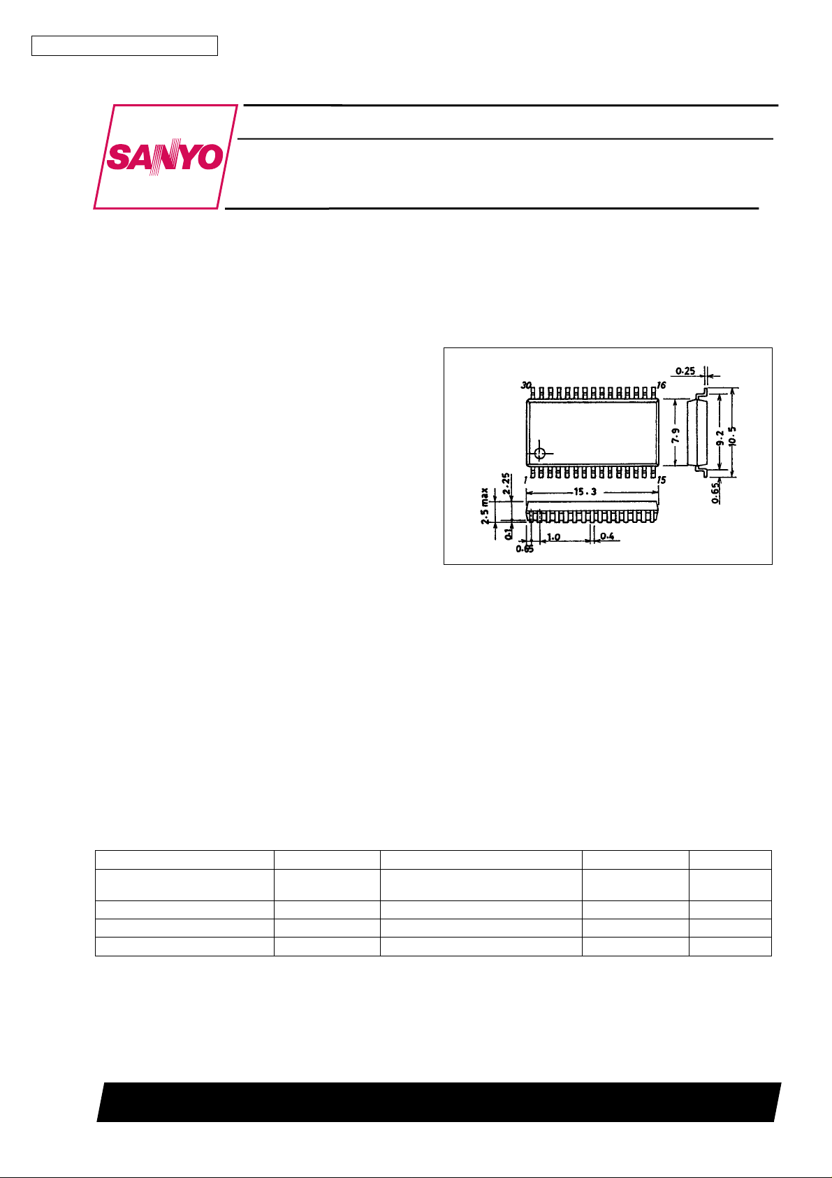
Package Dimensions
unit : mm
3073A-MFP30S
[LA2806M]
SANYO : MFP30S
Specifications
Maximum Ratings at Ta = 25°C
Parameter Symbol Conditions Ratings Unit
Maximum supply voltage V
Allowable power dissipation Pd max 800 mW
Operating temperature Topr –20 to +70 °C
Storage temperature Tstg –40 to +150 °C
P.V
CC
CC
max,
max
9V
SANYO Electric Co.,Ltd. Semiconductor Bussiness Headquarters
TOKYO OFFICE Tokyo Bldg., 1-10, 1 Chome, Ueno, Taito-ku, TOKYO, 110 JAPAN
O3097HA (II)/72495HA (ID)/3092HK/D111TS No.3852 - 1/11
LA2806M
Operating Conditions at Ta = 25°C
Parameter Symbol Conditions Ratings Unit
Recomended supply voltage V
Operating supply voltage range V
Recommended load resistance R
Preamplifier input voltage V
Operating Characteristics at Ta = 25°C, VCC=5V,f=1kHz
Parameter Symbol Conditions min typ max Unit
Quiescent current I
[Preamplifier]
Voltage gain VG
Total harmonic distortion THD
ALC turnover input voltage V
ALC output saturation voltage V
Equivalent input noise voltage V
ALC range ALC W
[Playback equalizer amplifier]
Voltage gain VG
Total harmonic distortion THD
Equivalent input noise voltage V
[Recording amplifier]
Voltage gain VG
Output bias voltage V
Total harmonic distortion THD –40 dBV preamplifier input 0.5 1.0 %
[LINE amplifier]: R
Voltage gain VG
Maximum output voltage V
=1kΩ
L
O
,P.V
CC
CC
op, P.VCCop 4.5 to 7.5 V
CC
L
IN
CC
–70 dBV input, measured between pins
C
5 and 8
Power amplifier 8 Ω
57 59 61 dB
–40 dBV input, measured between pins
5 and 8
Measured between pins 5 and 8 –68 –64 –60 dBV
ALC
–40 dBV input, measured between pins
OS
5 and 8
Input short circuited (internal 2.2 kΩ
NI
resistance)
From ALC ON to THD = 1 %
–70 dBV input, measured between pins
E
2 and 8
400 500 625 mVrms
40 45 dB
57 59 61 dB
–60 dBV input, measured between pins
2 and 8
Input short circuited (internal 2.2 kΩ
NI
resistance), Flat
50 kΩ impedance connected to pin 1
R
Z
, measured between pins 10 and 2
AC
100 kΩ resistance connected to pin 1
B
Z
, measured on pin 2
DC
Measured between pins 10 and 22 –1 0 +1 dB
L
–7.0 –4.0 –1.0 dB
0.4 0.8 1.2 V
5V
0 to 1.0 Vp-p
10 15 mA
0.5 1.0 %
1.5 5.0 µVrms
0.5 1.5 %
1.5 5.0 µVrms
Measured between pins 10 and 22,
max
THD = 1 % 0.6 Vrms
Total harmonic distortion THD –40 dBV preamplifier input 0.5 1.0 %
[Power amplifier]: R
Voltage gain VG
Output voltage P
Total harmonic distortion THD P
Input resistance r
Ripple rejection ratio SVRR Rg = 0, f
Output noise voltage V
=8kΩ, input pin 20
L
–30 dBV input, measured between pins
P
20 and 17
THD=10%
O
= 100 mW 0.5 1.0 %
O
i
Input short circuited, Flat 0.1 0.5 mVrms
NO
= 100 Hz, VCCr = –20 dBV 40 50 dB
r
26 28 30 dB
0.2 0.25 W
10 15 20 kΩ
[Voice-operated switch] Pin 25,R=20kΩapplied 5 V.
Sensitivity
V
V
–23 dBV input, f = 800 Hz 0.3 V
OXL
–27 dBV input, f = 800 Hz 4.5 5.0 V
OXH
Output ON voltage V sat 2 V supplied to pin24 0.3 V
[Control pin voltage]
1.5 (or
V
+ 0.3)
CC
1.5 V
CC
2.05 2.25 2.45 V
–0.7 V
Pin 26 to 30
Pin 24 (MUTE) V
[V
]
REF
Output voltage V
V
Input high-level voltage
H
V
Input low-level voltage 0 0.8 V
L
Input high-level voltage, supplied via
H
diode
REF
No. 3852 - 2/11
V
LA2806M
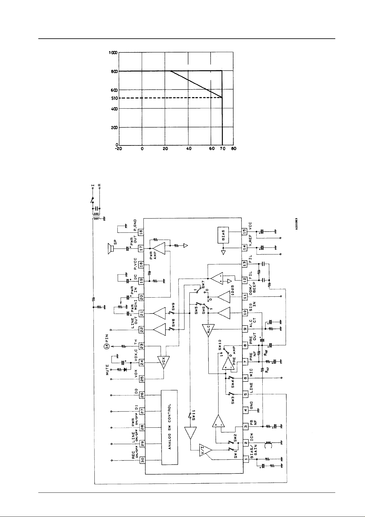
Pd max – Ta
Recommended mounting
Independent IC
Allowable power dissipation, Pd max – mW
Equivalent Block Diagram
Ambient temperature, Ta – °C
No. 3852 - 3/11
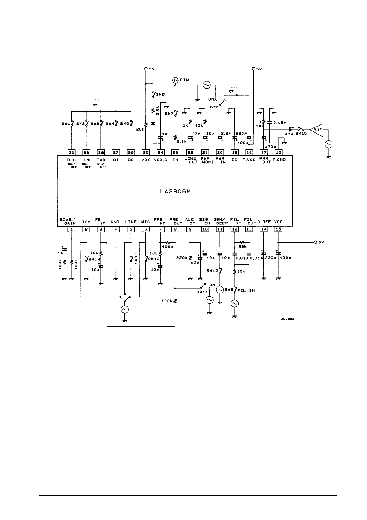
Test Circuit
LA2806M
Unit (resistance: Ω, capacitance: F)
No. 3852 - 4/11
 Loading...