

SANYO LA2650 Datasheet
Ordering number : EN5652
43097HA(OT) No. 5652-1/13
Overview
The LA2650 is a bass boost IC developed for use in minicomponent stereo systems, TV sets, and radio/cassette
player products. The cutoff frequency is determined by
external capacitors, and the boost gain, addition level, and
boost on/off state can be controlled by a microcontroller.
Features
• The bass boost gain is variable over a maximum range
of 20 to 35 dB in 5-dB steps, and the addition level into
the left and right channels can be controlled over a 0 to
–35 dB range in 3-dB and 5-dB steps. This allows an
optimal boost for the source and volume to be acquired
using microprocessor control.
• Includes two AGC circuits on chip: a level limiter (2 V
rms) for the maximum input in low-frequency boost
mode and a non-clipping limiter (i.e. clip prevention)
circuit.
• Can be switched between 2D and 3D systems.
Functions
• Variable boost gain (20, 25, 30, and 35 dB)
• Boost level limiter, non-clipping limiter
• Variable boost addition level (0, –3, –6, –9, –15, –20,
–25, and –35 dB)
• Left and right channel boost addition on/off
• Bass output pin for use in 3D systems
• Boost on/off
• LED on/off
• 8-bit serial microprocessor interface
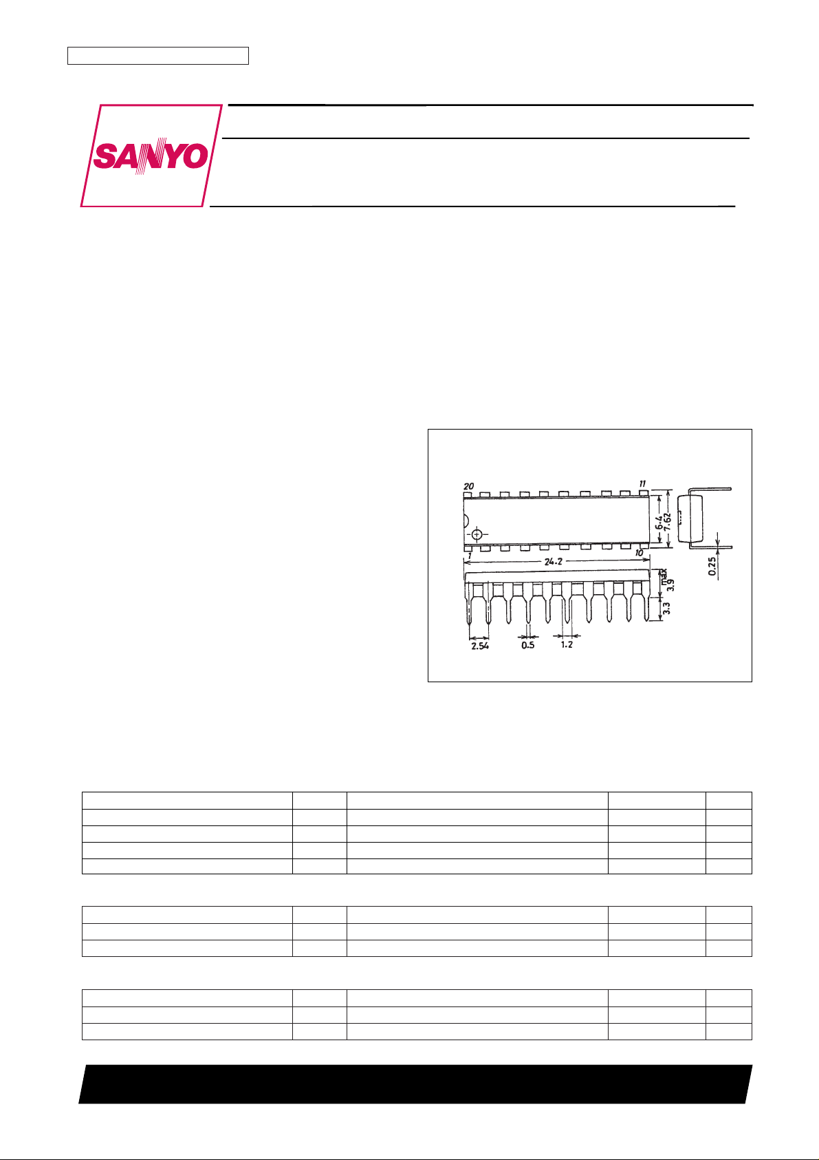
Package Dimension
unit: mm
3021B-DIP20
SANYO: DIP20
[LA2650]
LA2650
SANYO Electric Co.,Ltd. Semiconductor Bussiness Headquarters
TOKYO OFFICE Tokyo Bldg., 1-10, 1 Chome, Ueno, Taito-ku, TOKYO, 110 JAPAN
Bass Boost IC
Monolithic Linear IC
Parameter Symbol Conditions Ratings Unit
Maximum supply voltage V
CC
max 12 V
Allowable power dissipation Pd max Ta ≤ 70°C 450 mW
Operating temperature Topr –25 to +70 °C
Storage temperature Tstg –40 to +150 °C
Specifications
Maximum Ratings at Ta = 25°C
Parameter Symbol Conditions Ratings Unit
Recommended supply voltage V
CC
9V
Operating voltage range V
CC
op 5 to 10 V
Operating Conditions at Ta = 25°C
Parameter Symbol Conditions Ratings Unit
Low-level voltage V
IL
0 to 1.5 V
High-level voltage V
IH
3.5 to *5.5 V
Control Data Input Voltage Levels
Note: When VCCis under 5.7 V, the maximum value shall be VCC– 0.2 V.

No. 5652-2/13
LA2650
Parameter Symbol Conditions
Ratings
Unit
min typ max
Quiescent current
I
CCO
T Boost: off 5 8 13 mA
I
CCO
B Boost: on 6 9 14 mA
Voltage gain
VGT V
IN
= 0 dBm, Boost: off –2 0 +2 dB
VGB V
IN
= 0 dBm, Boost: on –2 0 +2 dB
BST1
Boost: on, f
i
= 50 Hz, BST = 35 dB,
25.5 28.5 31.5 dB
ADD = 0 dB, V
IN
= –30 dBm
BST2
Boost: on, f
i
= 50 Hz, BST = 35 dB,
21 24 27 dB
Boost level: high
ADD = 0 dB, V
IN
= –20 dBm
BST3
Boost: on, f
i
= 50 Hz, BST = 35 dB,
13 15 17 dB
ADD = 0 dB, V
IN
= –10 dBm
BST4
Boost: on, f
i
= 50 Hz, BST = 35 dB,
5 7 9 dB
ADD = 0 dB, V
IN
= 0 dBm
BST1
Boost: on, f
i
= 50 Hz, BST = 30 dB,
15 18 21 dB
ADD = –6 dB, V
IN
= –20 dBm
Boost level: low
BST2
Boost: on, f
i
= 50 Hz, BST = 30 dB,
8 10 12 dB
ADD = –6 dB, V
IN
= –10 dBm
BST3
Boost: on, f
i
= 50 Hz, BST = 30 dB,
1.5 3.5 5.5 dB
ADD = –6 dB, V
IN
= 0 dBm
Maximum output voltage
V
O
maxT THD = 1%, Boost: off 2.00 2.55 V
V
O
maxB THD = 1%, Boost: on 2.00 2.55 V
THD T
V
IN
= –10 dBm, Boost: off,
0.008 0.03 %
Total harmonic distortion
BPF = 400 Hz to 30 kHz
THD B
VIN= –10 dBm, Boost: on, fi= 50 Hz,
0.3 0.9 %
LPF = 30 kHz
CT T
VO= 0 dB, Rg = 10 kΩ, DIN AUDIO,
80 88 dB
Crosstalk
Boost: off
CT B
VO= 0 dB, Rg = 10 kΩ, DIN AUDIO,
50 59 dB
Boost: on
V
NO
T
Rg = 10 kΩ, JIS A, Boost: off,
–97 –90 dBm
Output noise voltage
Boost ADD = off
V
NO
B Rg = 10 kΩ, JIS A, Boost: on –91 –84 dBm
LED current I
LED
RED LED 11 15 19 mA
Electrical Characteristics at Ta = 25°C, VCC= 9 V, fi= 1 kHz, RL= 10 kΩ, BST = 35 dB, ADD = 0 dB, BST:ADD = ON
No. 5652-3/13
LA2650
Control Data for the Parameters in the Electrical Characteristics
*=don’t care
Parameter Conditions D1 D2 D3 D4 D5 D6 D7 D8
Quiescent current
I
CCO
T Boost: on L L L L L L L L
I
CCO
B Boost: off H H H H H H L H
Voltage gain V
IN
= 0 dBm
VG T Boost: off L L L L L L L L
VG B Boost: on H H H H H H L H
Boost level: high Boost: on, f
i
= 50 Hz, BST = 35 dB, ADD = 0 dB H H H H H H L H
Boost level: low Boost: on, f
i
= 50 Hz, BST = 30 dB, ADD = –6 dB H L H L H H L H
Maximum output voltage THD = 1%
V
O
maxT Boost: off L L L L L L L L
V
O
maxB Boost: on H H H H H H L H
Total harmonic distortion V
IN
= –10 dBm
THD T Boost: off, BPF = 400 Hz to 30 kHz L L L L L L L L
THD B Boost: on, f
i
= 50 Hz, LPF = 30 kHz H H H H H H L H
Crosstalk V
O
= 0 dBm, Rg = 10 kΩ, DIN AUDIO
CT T Boost: off L L L L L L L L
CT B Boost: on H H H H H H L H
Output noise voltage Rg = 10 kΩ, JIS A
V
NO
T Boost: off, Boost ADD = off L L L L L L L L
V
NO
B Boost: on H H H H H H L H
LED current
I
LED
RED LED * * * * * * H *
DC-CUT
VCA NF
5 to 10 V
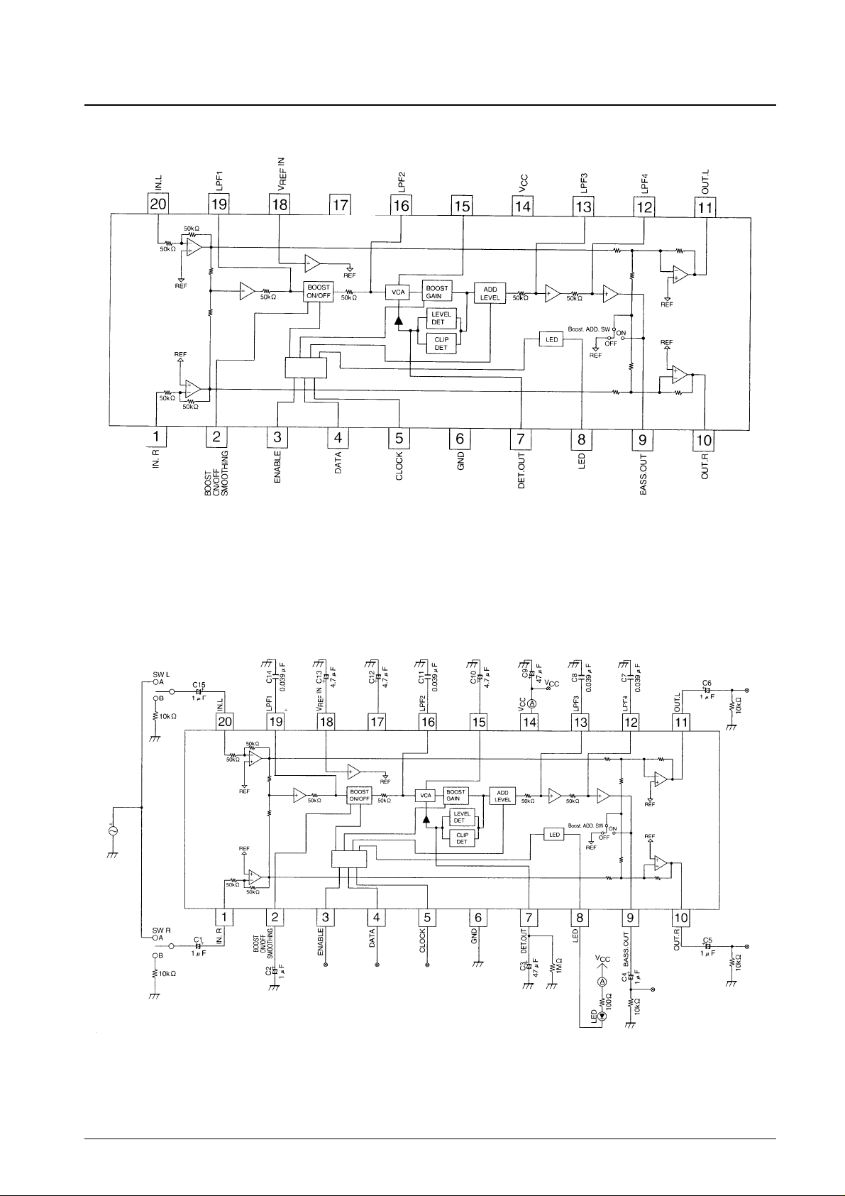
Block Diagram
No. 5652-4/13
LA2650
VCA NF
DC-CUT
DECODER
DECODER
Test Circuit
 Loading...