

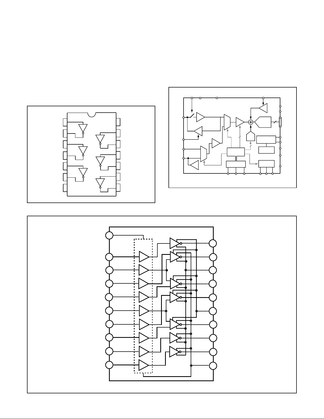
Page 1
SERVICE MANUAL
FILE NO.
Digital Disc Camera
Contents
1. iD PHOTO DISC ........................................................2
2. OUTLINE OF iD FORMAT DISC DRIVE CIRCUIT....4
3. OUTLINE OF CIRCUIT DESCRIPTION .................... 9
4. DISASSEMBLY........................................................20
5. ELECTRICAL ADJUSTMENT..................................24
6. MAC ADDRESS.......................................................29
7. TROUBLESHOOTING GUIDE.................................30
IDC-1000ZE
(Product Code : 126 250 01)
(U.K.)
IDC-1000ZEX
(Product Code : 126 250 02)
(Europe)
(General PAL area)
IDC-1000ZU
(Product Code : 126 250 03)
(U.S.A.)
(Canada)
8. PARTS LIST.............................................................31
ACCESSORIES & PACKING MATERIALS .............31
CABINET & CHASSIS PARTS 1 ............................. 32
CABINET & CHASSIS PARTS 2 ............................. 34
CABINET & CHASSIS PARTS 3 ............................. 35
ELECTRICAL PARTS ..............................................36
CIRCUIT DIAGRAM (Refer to the separate volume)
PRODUCT SAFETY NOTICE
The components designated by a symbol ( ! ) in this schematic diagram designates components whose value are of
special significance to product safety. Should any component designated by a symbol need to be replaced, use only the part
designated in the Parts List. Do not deviate from the resistance, wattage, and voltage ratings shown.
CAUTION
This product utilizes a laser.
The adjustment other than those specified herein may result in hazardous radiation exposure.
CAUTION : Danger of explosion if battery is incorrectly replaced.
Replace only with the same or equivalent type recommended by the manufacturer.
Discard used batteries according to the manufacturer’s instructions.
NOTE : 1. Parts order must contain model number, part number, and description.
Design and specification are subject to change without notice.
SX111/E, EX, U
2. Substitute parts may be supplied as the service parts.
3. N. S. P. : Not available as service parts.
REFERENCE No. SM5310255
Page 2
1. iD PHOTO DISC
1-1. iD PHOTO DISC HIGH-DENSITY TECHNOLOGY
The iD Photo Disc has a diameter of 5 centimeters and yet it
can store up to 730MB of information. A laser pulse magnetic
field modulation recording method and CAD-type ultra-high
magnetic resolution method have been used to record data
at a track pitch of 0.6 µm and an extremely short mark length
of 0.235 µ, which is smaller than the spot diameter of the
laser beam.
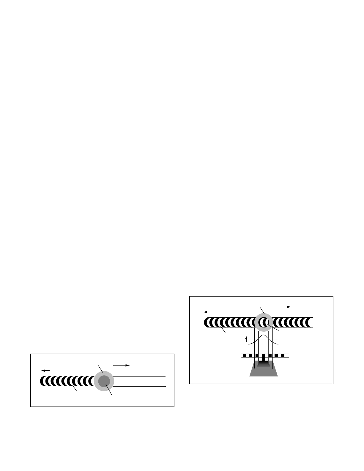
1-2. LASER PULSE MAGNETIC FIELD MODULA TION
RECORDING METHOD
The beam which is generated by the laser pickup in the iD
Photo disc drive focuses onto the disc recording medium as
a spot with a diameter of about 1 µm. During recording, a
mark with a diameter of 0.235 µm -- which is smaller than the
diameter of the laser beam spot-- is recorded. A “laser pulse
magnetic field modulation” recording method has been
adopted in order to achieve this. This recording method involves firstly a magnetic head which applies a magnetic field
which is modulated in accordance with the data supplied externally which is to be recorded. In this state, the laser beam
is directed to the reverse side of the disc. The radiated light
within an 0.6 µm-diameter area at the center of the beam
spot is momentarily heated to a temperature of around 200
degrees. The data is then recorded by means of the resulting
change in the magnetic polarity of the recording layer. The
recording mark which is made by this pulse-type laser beam
is accurately formed in the track at a diameter of 0.6 µm. The
rotation of the disc causes each recording mark to overlap
the preceding mark at a point 0.235 µm forward of the preceding mark. As a result, the circles formed according to the
state of the laser beam move along and leaves a continuous
series of minute crescent-shaped marks 0.235 µm across.
These marks are approximately one-quarter the size of the
recording marks which are made on other media such as CDs
and MOs. The iD Photo disc is a magneto-optical disc which
records data uses the principle of applying magnetism and
temperature sumultaneously so that the recording medium
can maintain its magnetic polarity. Because of this, the data
cannnot be erased simply by placing the disc within a magnetic field, and moreover the recording method does not result in any changes to the physical nature of the disc. This
means that stable characteristics can be maintained for respected disc writing operations.
recording laser beam
disc movement direction
1-3. CAD ULTRA-HIGH MAGNETIC RESOLUTION
METHOD
In order to play back the extremely small marks which have
been recorded using laser pulse magnetic field modulation,
the iD Photo disc uses a ultra-high magnetic resolution
method which incorporates CAD (Center Aperture Detection).
Ultra-high magnetic resolution is a form of technology in which
a magnetic signal taken from only the center of the spot is
extracted for playback. The iD Photo disc has a multi-layered structure which comprises a polycarbonate substrate,
upon which is the playback layer with magnetic characteristics, a recording layer which stores the data, and finally a
heat dispersion layer which rapidly allows the spot which has
been heated by the laser beam to cool. When data is played
back from the disc, the laser beam which is generated by the
pickup passes through the polycarbonate substrate to reach
the playback layer, and focuses on a 1-µm spot. This playback layer functions as a screen to shield the recording layer
on which the data is recorded from the laser beam, so that
only a 0.6 µm diameter area at the center of the laser beam
which reaches the playback layer passes through it and is
projected onto the magnetic recording area of the recording
layer by means of an increase in temperature (window). The
recorded data can be picked up and read through this “window”, and the surrounding area is shielded. Moreover, in general the spacing between the tracks is narrow and so signal
interference from tracks which are next to the track being read
can occur. However, CAD-type ultra- high magnetic resolution also solves this interference problem. With CAD-type ultra-high magnetic resolution, only the magnetic signal which
passes throught the window at the center of the beam spot is
read, so that the playback reading area can be restricted to a
very narrow area not only in the tracking direction, but also in
the transverse direction. As a result, signal interference is
suppressed, and the spacing between the tracks can also be
made smaller.
playback laser beam
disc movement direction
MO pit
0.235µm
T
ultra-high magnetic
resolution window
value
temparature
distribution
recording layer
playback layer
Fig. 2
MO pit
0.235µm
recording spot
Fig. 1
– 2 –
Page 3

1-4. PRML SIGNAL PROCESSING
When the data on the iD Photo disc is read, the 0.235 µm
overlapping recording marks which are made during laser
pulse magnetic field modulation recording are read through
an 0.6 µm window by means of a CAD-type ultra-high magnetic resolution reading method. Because this window has a
diameter of 0.6 µm, at least two or three recording marks can
be viewed through this window at any given time. With the iD
Photo disc, PRML signal processing has been adopted as
the signal processing method for this readable area. PRML
signal processing compares the signal wave pattern which is
detected when recording marks with several different pattern
types pass by the window with the signal wave pattern which
is actually obtained by the pickup in order to recreate the
data which has actually been recorded. This technology makes
it possible to accurately reproduce the recording marks which
are smaller than the window being used to read them, and if
a signal pattern which is not valid is read, then it is handled
as an error. In this way, recording and playback of data at
high densities can be couple with high data reliability.
1-5. ZCLV METHOD OF ROTATION CONTROL
A ZCLV (Zoned Constant Linear Velocity) method of rotation
control has been adopted for the iD Photo disc. The ZCLV
method increases the disc rotation speed on a zone basis in
accordance with the progression toward the center of the disc
as the speed of rotation of the disc recording surface with
respect to the pickup becomes progressively slower. The iD
Photo disc is devided into 12 bands from the outside to the
inside of the disc surface, and the rotation speed within each
band is varied within a range of 1900-3100 rpm in order to
maintain the speed of rotation of the recording surface with
respect to the pickup to a level of about 5 meters per second.
1-6. EXTERNAL CLOCK SIGNAL
The iD Photo disc uses an external clock method to gener-
ate the clock pulses which are used to regulate the timing for
reading and writing of data. With conventional methods, the
clock pulse is generated based on changes in the data being
read. However, with this external clock method, an FCM (Fine
Clock Mark) signal is created beforehand and recorded onto
the disc for use as a reference signal in order to generate the
clock pulse. The timing of this FCM signal is monitored during reading of data in order to control the oscillation frequency
of the clock signal generator in accordance with the rotation
of the disc. The Fine Clock Mark is engraved accurately onto
the disc when the disc is manufactured, and it can then be
used as an accurate reference for stable reading and writing.
– 3 –
Page 4
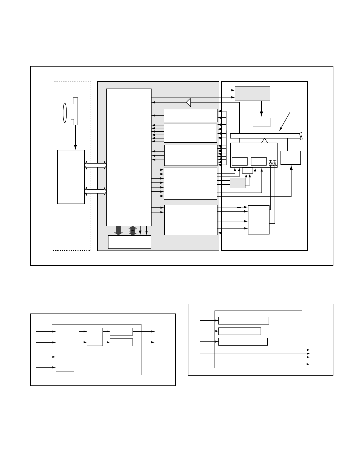
2. OUTLINE OF iD FORMAT DISC DRIVE
CIRCUIT
1. OUTLINE OF DRIVE CIRCUIT BOARD
A drive part is composed of the block diagram of the Fig. 1,
and a drive circuit board is composed of MC1, MC2 and MC3.
CAMERA
CAMERA
ASIC
CA2
CPU
Processor
BUS
ATA BUS
(IDE)
50øAS-MO DRIVE CIRCUIT BOARD (MC3)
WDTX(reverse of WDT)
(A/D) THERMO
MO signal (play signal)
(A/D) FCLKAMPL
(A/D) ADRSAMPL
DRIVE
ASIC
(PWM output) FCSR
(PWM output) FCSF
(PWM output) TRKR
(PWM output) TRKF
(PWM output) SLDR
(PWM output) SLDF
SDRAM
(64Mbit)
FCLKNP
FCLKPP
FCLKZ
ADRSPLS
(A/D) FES
(A/D) TES
(A/D) SUM
SPREF
16bit
WDT
WCLK
WG
SDCLK
96
168
167
186
136
190
161
160
162
163
189
193
192
191
209
208
212
211
207
206
205
165
171
"0" Rec
"1" Play
RF Amplifier
FCM/ADDR
Amplifier
Servo
Amplifier
Servo
Driver
(BD6603KVT)
Lazer POWER
Control
(TA6015F)
MAGNETIC HEAD
DRIVER CIRCUIT
THERMO
I
J
Photo
A
sensor
B
output
C
D
A
Temparature
B
sensor
C
D
E
F
Tracking
G
H
actuator
T+
T-
SLED+
SENSOR
SLED-
BOARD
(MC2)
F+
F-
U/V/W/COM
Iout
LD-ON/Off
RF-On/Off
(oscillation circuit
On/Off)
PS-On/Off(Power
saveOn/Off)
ST(abnormal
detection)
BOARD (MC1)
Magnetic
head
Pick Up
Focus
actuator
Sread
motor
Laser
APC IC
(included
PICK UP)
DRIVE MECHA and
MECHA CIRCUIT
BOARD
iD disc(50ø)
Spindle
VCC
motor
LD
PD
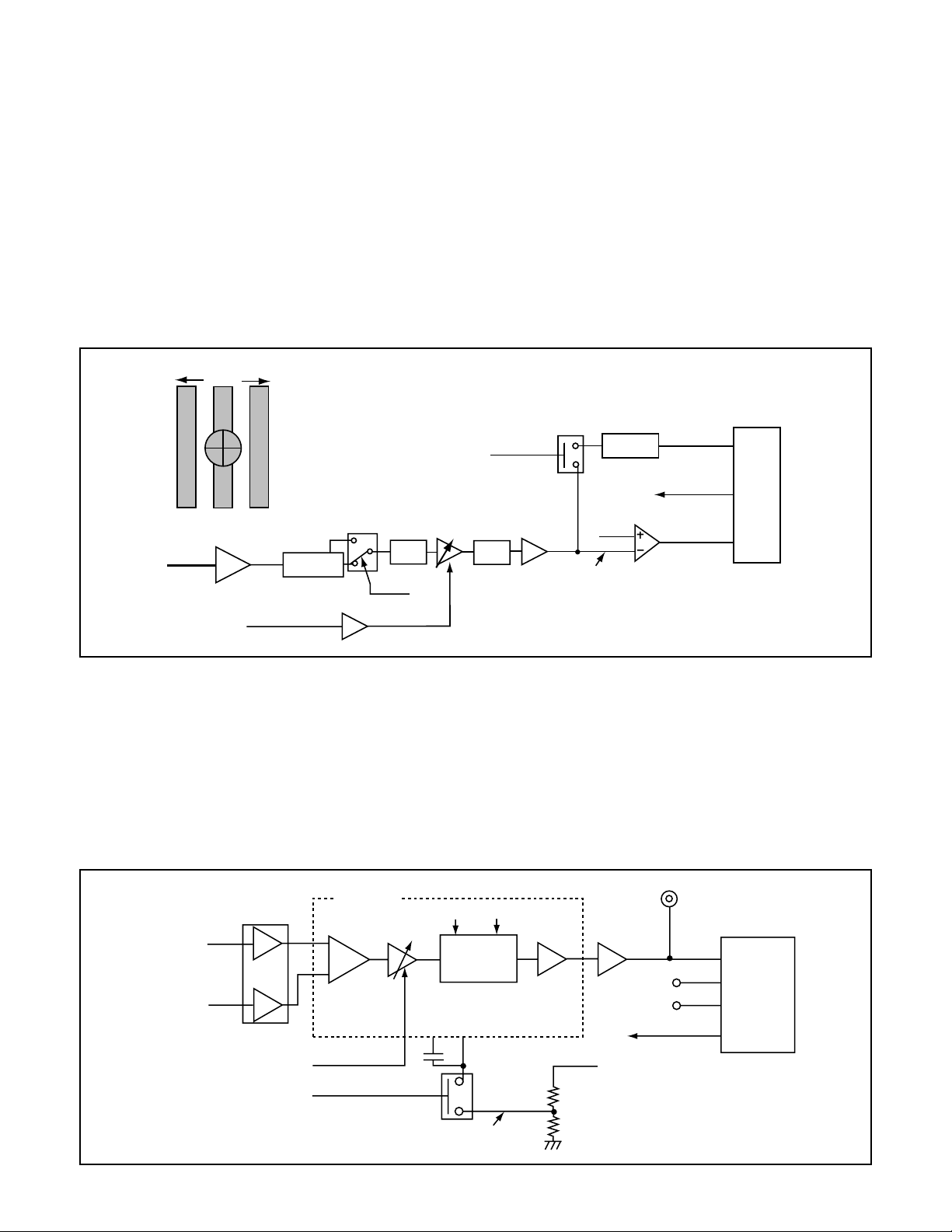
2. OUTLINE EXPLANATION OF DRIVE CIRCUIT
BOARD
2-1. MAGNETIC HEAD DRIVER CIRCUIT BOARD (MC1)
During recording, it is the driver circuit board to magnetize
toward the magnetic head.
WD_P
WD_N
EJULK
EJLK
Large current
buffer
Magnetic
head
UP/DOWN
sensor
FET array
Amplitude
limitation circuit
Amplitude
limitation circuit
+ MH+
- MH-
MC1
2-1-1. EXPLANATION OF OPERATION
During recording, the data (WD_P and WD_N) from the MC3
circuit board is used to operate the large current buffer at IC801
in order to turn the FET array on and off. This is turn determines the direction of the magnetic field applied to the magnetic head. Also an upper limit is decided so that a magnetic
field level may not be bigger at the amplitude limitation circuit
by the data.
To the
magnetic
head
To the
magnetic
head
Fig. 2
The ascent and descent condition of the magnetic head is
being watched with the magnetic head up and down sensor.
2-2. SENSOR CIRCUIT BOARD (MC2)
WRPROT
CARTRG
PUINI
SPDLW
SPDLU
SPDLV
SPDLCOM
S8003
Disc write protect detection switch
S8004
Disc setting detection switch
D8003
Pick up location detection sensor
MC2
2-2-1. EXPLANATION OF OPERATION
Sensor circuit board (MC2) is the relay circuit board for the
disc write protection detection, disc setting detection switch,
the pickup location detection sensor and spindle motor control signal.
– 4 –
Fig. 1
To the
spindle
motor
Fig. 3
Page 5
2-3. OUTLINE EXPLANA TION FOR EACH BLOCK OF
DRIVE CIRCUIT BOARD (MC3)
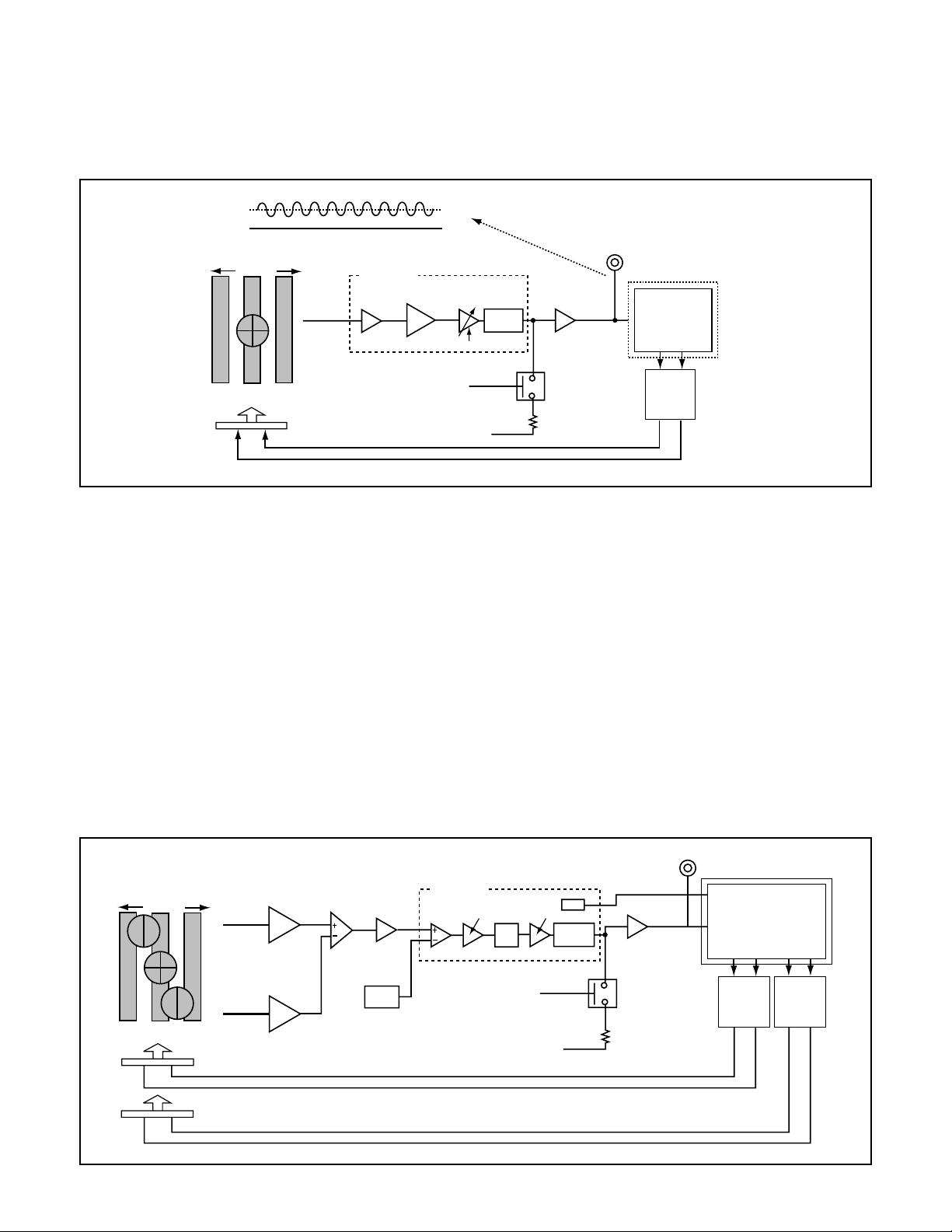
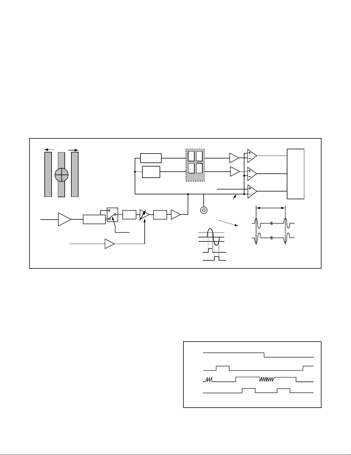
2-3-1. SERVO AMPLIFIER
They are amplifier part for the focus servo and the tracking
servo.
1. FOCUS SERVO (DISC SURF ACE RUNOUT TRACKING CONTROL)
Servo control is carried out by the DSP which is built into the
ASIC (IC402). This controls the focus actuator of the pickup in
order to carry out surface runout tracking control.
Minute
amplitude
inside
Land
Groove
C
B
Land
D
A
Groove
outside
Land
A, B, C, D
Focus
actuator
IC831
SSI33P3721
Gain-Amp
(x1.4)
2.5V
GND
FES Matrix
[Kf(A+C)-(B+D)]
AGC on/off
1. Focus offset adjustment
When the servo and laser are both off, the DSP of the ASIC
(IC402) samples the FE (focusing error) signal and obtains
average values which are used to control the offset cancel
registers of SSI33P3721 (IC402) in order to cancel the electrical offset. The signal level is set to 2.5 V DC.
2. Focus gain adjustment
The DSP of the ASIC (IC402) carries out focus searching to
measure the peak levels (+/–) for the S-shaped characteristics of the FE signal, and sets the ABCD gain (focus gain) for
the SSI (IC831) in accordance with these values. The above
The S-shaped curve amplitude of the focus error signal
(FE signal) is TYP 1.2Vp-p
Focus error singal
observation terminal
(TP810)
IC815
DRIVE ASIC
MACRO
FES
PWM 3/4
FCSF FCSR
4
IN2R
IN2F
H2F
H2R
OUT
OUT
14
DSP
5
12
The OA amplifiers and power supply
of the analog switches are all 5V.
AGC
WG
"0" REC
"1" PLAY
OFFSET
CANCEL
2.5V
Gain-Amp
Read (x1.22)
Write (x0.76)
IC835
(AD8532)
IC833
(ADG702)
FES
BD6603KVT
ABCD gain for the SSI is adjusted by the microprocessor in
order to maintain the VPP for the S-shaped characteristics of
the FE signal to approximately 1.18 V. The ABCD gain for the
SSI can be adjusted within the range of x1.2 to x4.3. During
recording (when the laser is at high power), the signal amplitude is reduced by about half before the FE signal is input to
the DSP of the ASIC (IC402).
3. Focus servo ON
The DSP of the ASIC (IC402) moves the focus actuator up
and down to control the FE signal so that its AC component is
“0”.
Fig. 4
2. TRACKING SERVO (MAIN PP AND PP SUBTRACTION METHOD)
Servo control is carried out by the DSP which is built into the
ASIC (IC402). This controls the tracking actuator and the thread
inside
Land
Groove
HF
C
B
Land
D
A
E
Groove
outside
G
Land
Tracking
actuator
Sread
actuator
A, B, C, D
E, F, G, H
Main Beam PP
[(A+D)-(B+C)]
IC814
(AD8054)
Sub Beam PP
α[(F+G)-(H+E)]
IC814
(AD8054)
IC814
(AD8054)
Gain-Amp
(±6dB)
IC837
(AD8051)
Offset
adjustment
SSI33P3721
2x[(A+D)-(B+C)]α[(F+G)-(H+E)]
actuator of the pickup in order to carry out rotation offset tracking control.
Tracking error signal
observation terminal
(TP811)
LPF
Gain-Amp
(x1~x2.2)
WG
"0" REC
"1" PLAY
TZC
OFFSET
CANCEL
2.5V
TZC
Buf
IC835
(AD8532)
IC834
(ADG702)
TES
IC815
BD6603KVT
TZC
(tracking
zero cross)
FES
PWM 5/6
TRKFTRKR
2
IN1R
IN1F
H1F
OUT
9
3
H1R
OUT
7
MACRO
PWM 1/2
SLDF
36
IN4F
H4F
OUT
40
DSP
SLDR
– 5 –
35
IN4R
H4R
OUT
42
Fig. 5
Page 6
1. Tracking offset adjustment
When the servo and laser are both off, the DSP of the ASIC
(IC402) samples the TE (tracking error) signal in order to control the offset cancel of SSI33P3721 (IC831) in order to cancel the electrical offset.
2. Tracking gain adjustment
When the focus servo is on, the DSP of the ASIC (IC402)
measures the amplitude of the TE signal and uses it to set
the CGA amp gain of the SSI (IC831).
2-3-2. FCM/ADDR AMPLIFIER
1. FCM AMPLIFIER
FCM is an abbreviation for Fine Clock Mark. This is used as
the external clock reference to generate the signal which becomes the syncronizing standard for the drive circuit board.
3. Balance adjustment of main PP and sub PP
This measures the DC offset when shifting to the inside and
to the outside occurs, with respect to the center of the TE
signal when the actuator is shifted 0.83 V to the outside, when
it is shifted 0.83 V to the inside and when it is at the standard
position.
4. Servo ON (disc rotation offset tracking)
The DSP of the ASIC (IC402) moves the tracking actuator to
the left or right to control the TE signal so that its AC component is “0”.
inside
Land
Groove
A, B, C, D
outside
C
D
B
A
Land
Groove
IC814
(AD8054)
TPP Matrix
[(A+B)-(C+D)]
The OA amplifiers, analog switch
and the power supply of the
comparator IC are all 5V.
Land
IC854
(AD8054)
Attenuator
gain fixing
play: x 6.356
rec: x 3.33
FCLKGC
IC855
(ADG701)
Amp
IC857
(AD8534)
LC
Filter
WG
"0" REC
"1" PLAY
PEAK HOLD
circuit
BOTTOM
HOLD
circuit
VCA variable
range (± 4dB)
Ctrl
IC853
(BA7655)
FCLKAMPBTM
LC
Filter
1. Fine clock mark (FCM)
A computation ((A+B)–(C+D)) is carried out on the signals
from the photosensor, after which they pass through the VCA
circuit (IC853) and LPF circuit, and then the FCM signal amplitudes pass through the peak hold and bottom hold circuits
and are input to the DSP of the ASIC (IC402), where A/D
conversion is carried out. At the DSP of the ASIC (IC402), the
D/A value of the signal (FCLKGC) which has had the control
voltage adjusted by the VCA (IC853) is changed so that the
FCM level is set to the level which is necessary for the
FCLKNP and FCLKPP signals to be generated. Furthermore,
DSP of the ASIC (IC402) and the above circuits set the slice
level to 50 % - 70 % of the +/– side FCM marks so that the
comparator (IC852) (FCLKPP and FCLKNP) singals do not
delay the transfer of the address signals. The above circuits
adjust the signals so that the FCM amplitude is at about the
same level when at the default recording and playback power.
Furthermore, a ratio of 60 % or more between the + side and
the – side of the FCM signal is necessary when LAND is on
and when GROOVE is on. The DSP controls the control potential of the VCA (IC853) so that the Vpp of the FCM signal
is about TYP 1.7 Vp-p. Furthermore, the signal interval for
the FCM signals is 532 x 50 ns = 26.6 µs.
FCLKAMPL
Gain-Amp
x2
IC854
(AD8054)
upper slice level
lower slice level
ASIC
D/A
A/D
D/A
A/D
DSP process
FCMK signal
obwervation
LAND
FCM
FCLKPP
FCLKNP
FCLKSLS
FCLKSLSBTM
IC857
(AD8534)
VC25
termanal
(TP808)
IC851
(AD8534)
primary
function
circuit
primary
function
circuit
comparator
input allowable
value (0.8~3.6V)
LAND
FCM
2.5V
GROOVE
Comparator
FCM-PP
IC852
(LT1721)
Comparator
FCM-NP
IC852
(LT1721)
Comparator
FCM-Z
IC852
(LT1721)
26.6[µs]
AS-MO ASIC
160
FCLKPP
161
FCLKNP
162
FCLKZ
2.5V
2.5V
Fig. 6
2. FCLKPP/FCLKNP/FCLKZ
These are generated from the FCM signal by the comparator
(IC852) according to the timing shown in Fig. 7.
1. When LAND is on, the lead channel macro of the ASIC
judges that a FCM has been detected after the FCLKPP
signal has been detected and the FCLKZ signal is rising.
2. When GROOVE is on, the lead channel macro of the ASIC
judges that a FCM has been detected after the FCLKNP
signal has been detected and the FCLKZ singal is falling.
LAND
FCLKPP
FCLKZ
FCLKNP
GROOVE
Fig. 7
– 6 –
Page 7
3. The principle of rec/play clock generated by the PLL
The clock is reproduced by the PLL with respect to the signal
which has been detected to be the FCM signal by the circuit
(primary function circuit) which generates the slice level from
the FCM signal. The frequency of the reproduced clock is 20
MHz.
4. LC filter
LC filters are located before and after the VCA (IC853). During recording, there is the possibility that the WCLK (20 MHz)
or other high-frequency interference can become mixed in with
2. ADDRESS DETECTION/AMPLIFIER
Mainly the address detection of the disc and signal process in
order to detect are done.
the FCM signal or the address signal. These LC filters remove
almost all of the signal components which are at 20 MHz or
above, leaving just the base frequencies (2-3 MHz) for the
FCM and address signals.
5. Peak hold for FCM signal and bottom hold circuit
These circuits use the amplitude modulation of the FCM signal to hold the peak level and the bottom level of the FCM
signal at the capacity which is connected to the transistor
emitter.
outside
Land
Groove
A, B, C, D
inside
C
D
B
A
Land
Groove
IC814
(AD8054)
Main Matrix
[(A+D)-(B+C)]
Land
ADRSGC
The OA amplifiers, analog switch
and the power supply of the comparator
IC are all 5V.
IC856
IC854
(AD8054)
Attenuator
Gain fixing
Read: x 6.81
Write: x 3.78
(ADG701)
IC857
(AD8534)
Amp
LC
Filter
WG
"0" REC
"1" PLAY
VCA
variable range
(± 4dB(min))
1. Address detection
The main PP signal ((A+D)–(B+D)) at the tracking servo amplifier shown in Fig. 5 passes through the VCA circuit (IC853)
and the LPF circuit, after which the address peak signal is
input to the DSP of the ASIC (IC402) and A/D conversion is
then carried out. As a result, the maximum amplitude of the
address signal is detected and the control potential of the VCA
AS-MO ASIC
189
173
163
A14
A02
ADRSPLS
Filter
Ctrl
IC853
(BA7655)
FCLKWIN
Gain-Amp
LC
IC859
(ADG702)
IC854
(AD8054)
PEAK HOLD
CIRCUIT
Comparator
VC25
comparator
input allowable value
(0.67~3.36V)
ADRSAMPL
ADRSGC
ADRSPLS
IC852
(LT1721)
(IC853) is changed so that the amplitude of the address signal can be changed to the appropriate level. Furthermore, it is
input to the comparator (IC852) to generate the address signal. This address signal is taken up by the DC macro of the
ASIC (IC402) to be used as the frame address and track address during recording and playback.
Fig. 8
2-3-3. RF AMPLIFIER
RF is the data signal that it is to be read by a pickup sensor (I, J).
Gain-Amplifier
x 8.17
I
J
IC838
(AD8062)
I/J is bias by 2.5 V (FREF).
SSI33P3721
Cutoff
AGC
Programmable
AGC on/off
MOAGCHLD
AGCOFFH
Boost
Equalizer
Filter
IC836
(ADG701)
During AGC OFF
Gain is decided.
– 7 –
+5VA
MO-RF
IC832
(AD8051)
2.0V
1.0V
AGCOFFH
TP801
(MO observation)
AS-MO ASIC
136
RF
137
REFTOP
138
REFBTM
221
P06
Fig. 9
Page 8
The signals from the sensors (I/J) are pre-amplified by the
gain amplifier, and then pass through the AGC/equalizer of
the SSI (IC831), and are then input to the RF signal terminal
of the ASIC (IC402). The AGC control signal (AGCOFFH) from
the ASIC (IC402) is modulated to control the on/off status of
the AGC. When the AGC is on, the wave pattern monitored at
TP801 is adjusted to a constant amplitude.
2-3-4. SERVO DRIVER
The driver circuit of spindle motor, sread motor and each actuators are accumulated inside BD6603KVT (IC815). The
spindle motor is used three aspect sensorless motor (DC
motor).
2-3-5. LASER POWER CONTROL
TA6015F (optical disc power control (LPC): IC841) and
TA6012F (optical disc high speed APC) are used in the pairs.
An APC IC appears on the pickup. LPC (IC841) control makes
it possible to set characteristics such as playback power, recording peak power, duty, laser on/off setting and low power
consumption standby mode using the register settings of the
LPC (IC841).
3. BLOCK DIAGRAM OF PLAY/REC AND SIGNAL PROCESS etc.
APC IC (on the pickup)
The APC IC functions to maintain the current detected by the
photosensor attached to the laser to a constant level. This
has the effect of canceling any fluctuations in characteristics
resulting from the semiconductor laser temparature, and any
variances in production lots, so that the laser power can be
maintained at a stable level. The ON/OFF laser high-frequency
currents, power save and laser are output open corrector from
LPC IC, and input to APC IC.
Superimposing high-frequency currents
When a high-output semiconductor laser is used, interference
can be generated from the light which is reflected back from
the disc. Because of this, high-frequency currents of 300-600
MHz are superimposed on the laser drive currnet to reduce
interference.
2-3-6. SDRAM
This is used as a WORK for ECC encoding and decoding, as
a buffer for seamless recording and playback, and as a drive
cache.
Magnetic field strength
MH
Driver
SSI
IC
Gain
G.C
Gain
G.C
DRIVE ASIC
A/D
2T signal
PLL
Slice Level
ADRS
Dec.
SH
APC
IC
LPC
IC
EQ, fc, Boost
MO
FCM
Adrs
WCLK
Duty Pr Pw
Temparature
sensor
1. Playback clock by PLL
The playback clock (20 MHz) which is generated from the
FCLKPP/FCLKNP signals (see Fig. 7) obtained from the FCM
is played back. The spindle motor operation is controlled by
CL V (constant linear velocity) to provide a constant FCM cycle
(26.6 µs). Accodingly, the rotation becomes faster as tracking
moves toward the center of the disc.
RCLK
Tap coefficient
Digital
EQI
Delay
Off Track
Tilt Mark
CPU
Delay
quantity
Expectation
value
PRML
PR(1, 1)
2T/8T
amplitude
ratio
ECC
Fig. 10
– 8 –
Page 9
3. OUTLINE OF CIRCUIT DESCRIPTION
10
9 6 5 4 3 2 1
13
14 15 16 17
18
19
20
G
R
G
R
G
R
B
G
B
G
B
G
G
R
G
R
G
R
B
G
B
G
B
G
Vertical register
Horizontal register
Note
Note: Photo sensor
VOUT
GND
NC
NC
V
ø3
øSUB
NC
C
SUB
NC
V
L
øRG
12
GND
11
VDD
7
GND
8
NC
V
ø2B
Vø2A
Vø1
Hø1
Hø2
3-1. CA1 CIRCUIT DESCRIPTION
Around CCD block
1. IC Configuration
IC903 (ICX267) CCD imager
IC902, IC904, IC908 (74ACT04MTC) H driver
IC907 (CXD3400N) V driver
IC905 (AD9803) CDS, AGC, A/D converter
2. IC903 (CCD)
[Structure]
Interline type CCD image sensor
Optical size 1/2 type
Effective pixels 1392 (H) ×1040 (V)
Pixels in total 1434 (H) ×1050 (V)
Actual pixels 1360 (H) × 1024 (V)
Optical black
Horizontal (H) direction: Front 2 pixels, Rear 40 pixels
Vertical (V) direction: Front 8 pixels, Rear 2 pixels
Dummy bit number Horizontal : 20 Vertical : 3
Pin 1
2
V
2
Pin 11
Fig. 1-1.Optical Black Location (Top View)
Pin No.
1
2, 3
4
5, 6, 8,
14, 16
7, 9, 12
10
11
13
15
Symbol
Vφ
φSUB
V φ
1
2A, Vφ2B
V φ3
NC
GND
VOUT
VDD
CSUB
8
H
40
Pin Description
Vertical register transfer clock
Vertical register transfer clock
Vertical register transfer clock
GND
Signal output
Circuit power
Substrate clock
Substrate bias
Waveform
GND
DC
DC
Fig. 1-2. CCD Block Diagram
Voltage
-8.0 V, 0 V
-8.0 V, 0 V, 15 V
-8.0 V, 0 V
0 V
Aprox. 7 V
15 V
Different from every CCD
Different from every CCD
17
18
19
20
VL
φRG
H φ
H φ
Protection transistor bias
1
2
Reset gate clock
Horizontal register transfer clock
Horizontal register transfer clock
DC
Table 1-1. CCD Pin Description
– 9 –
-8 V
12 V, 17 V
0 V, 5 V
0 V, 5 V
When sensor read-out
Page 10
3. IC902, IC904, IC908 (H Driver) and IC907 (V Driver)
An H driver and V driver are necessary in order to generate
the clocks (vertical transfer clock, horizontal transfer clock
and electronic shutter clock) which driver the CCD.
IC902, IC904 and IC908 are inverter IC which drives the horizontal CCDs (H1 and H2). In addition the XV1-XV3 signals
which are output from IC102 are the vertical transfer clocks,
and the XSG1 and XSG signal which is output from IC102 is
superimposed onto XV2A and XV2B at IC907 in order to generate a ternary pulse. In addition, the XSUB signal which is
output from IC102 is used as the sweep pulse for the electronic shutter, and the RG signal which is output from IC102
is the reset gate clock.
14
CC
1A
1Y
2A
2Y
3A
1
2
3
4
5
V
13
6A
12
6Y
11
5A
10
5Y
4. IC905 (CDS, AGC Circuit and A/D Converter)
The video signal which is output from the CCD is input to Pin
(30) of IC905. There are S/H blocks inside IC905 generated
from the XSHP and XSHD pulses, and it is here that CDS
(correlated double sampling) is carried out.
After passing through the CDS circuit, the signal passes
through the AGC amplifier. It is A/C converted internally into
a 10-bit signal, and is then input to IC102 of the CA2 circuit
board. The gain of the AGC amplifier is controlled by serial
data which is output from IC102 of the CA2 circuit board.
PBLK
CCDIN
CLPDM
AUX1IN
AUX2IN
AVDD
CDS
CLP
CLP
4 dB
MUX
AVSS
2~36 dB
2:1
VGA
MUX
10
BUF
2:1
CONTROL
REGISTERS
DIGITAL
INTERFACE
Offset
DAC
8
CLPOB
AD9840
CLP
10-BIT
ADC
BANDGAP
REFERENCE
INTERNAL
BIAS
INTERNAL
TIMING
DRVDD
DRVSS
10
DOUT
VRT
VRB
CML
DVDD
DVSS
4A
3Y
GND
6
7
9
4Y
8
Fig. 1-3. IC902, IC904 and IC908 Block Diagram
DD
V
1
Input
Buffer
XSHT
2
XV3
3
XSG3B
4
XSG3A
5
XV1
6
XSG1B
7
SDATA
SCK
SL
SEN
Fig. 1-5. IC905 Block Diagram
SHT
20
V3B
19
V
L
18
V3A
17
V1B
16
V
H
15
V1A
14
DATA
SHDSHP
CLK
8
9
10
XSG1A
XV4
XV2
Fig. 1-4. IC907 Block Diagram
– 10 –
V4
V2
GND
13
12
11
Page 11
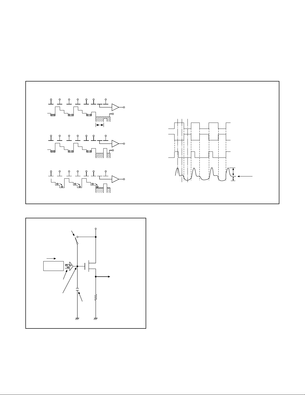
5. Transfer of Electric Charge by the Horizontal CCD
The transfer system for the horizontal CCD emplays a 2-phase drive method.
The electric charges sent to the final stage of the horizontal CCD are transferred to the floating diffusion, as shown in Fig. 1-6.
RG is turned on by the timing in (1), and the floating diffusion is charged to the potential of PD. The RG is turned off by the timing
in (2). In this condition, the floating diffusion is floated at high impedance. The H1 potential becomes shallow by the timing in (3),
and the electric charge now moves to the floating diffusion.
Here, the electric charges are converted into voltages at the rate of V = Q/C by the equivalent capacitance C of the floating
diffusion. RG is then turned on again by the timing in (1) when the H1 potential becomes deep.
Thus, the potential of the floating diffusion changes in proportion to the quantity of transferred electric charge, and becomes
CCD output after being received by the source follower. The equivalent circuit for the output circuit is shown in Fig. 1-7.
(1)
H1 H2 H1 H2 H1 HOG RG
CCD OUT
Floating diffusion
(2)
H1 H2 H1 H2 H1 HOG RG
PD
PD
CCD OUT
H1
H2
RG
15.5V
(1) (2) (3)
3.5V
0V
3.5V
0V
12V
(3)
H1 H2 H1 H2 H1 HOG RG
Fig. 1-6. Horizontal Transfer of CCD Imager and Extraction of Signal Voltage
Reset gate pulse
Direction of transfer
H Register
Electric
charge
Floating diffusion gate is
floated at a high impedance.
C is charged
equivalently
12V Pre-charge drain bias(PD)
Voltage output
Fig. 1-7. Theory of Signal Extraction Operation
CCD OUT
CCD OUT
RG pulse peak signal
Signal voltage
6-2. Iris drive
When in the aperture enable (AE SW) state, the target aperture value signal (IRIS PWM) which is output by the ASIC and
the aperture value signal (HALL OUT +/–) which is output by
the lens are compared so that feedback control can be carried
out.
6-3. Focus drive
When the drive signals (FRSTB, FCW, FOEB and FCLK) which
are output from the ASIC, the focus stepping motor is sinewave driven by the micro-step motor driver (IC953). Detection
of the standard focusing positions is carried out by means of
the photointerruptor (FOCUS PI) inside the lens block.
6-4. Zoom drive
When the drive signals (ZRSTB, ZCW, ZOEB and ZCLK) which
are output from the ASIC, the zoom stepping motor is sinewave driven by the micro-step motor driver (IC954). Detection
of the zoom positions is carried out by means of photoreflector
(ZOOM PI) inside the lens block.
Black level
6. Lens drive block
6-1. Shutter drive
The shutter drive signal (SHUTTER) which is output by the
ASIC and the aperture enable signal (AE SW) cause a positive and negative voltage are applied to the aperture drive coil
to open and close the lens aperture.
6-5. ND filter drive
When the drive signals (ND ON, ND OFF) which are output
from the ASIC, ND filter opens and closes.
– 11 –
Page 12

3-2. CA2 CIRCUIT DESCRIPTION
1. Circuit Description
1-1. Scannning converter (Interlace converter)
This circuit uses the function of a 64-Mbit SDRAMs to convert the non-interlaced signal which is output from the CCD
into an interlaced signal for the video monitor.
1-2. Camera signal processor
This comprises circuits such as the digial clamp circuit, white
balance circuit, γcircuit, color signal generation circuit, matrix circuit and horizontal aperture circuit.
1. Digital clamp circuit
The optical black section of the CCD extracts 16-pixel averaged values from the subsequent data to make the black level
of the CCD output data uniform for each line. The 16-pixel
averaged value for each line is taken as the sum of the value
for the previous line multiplied by the coefficient k and the
value for the current line multiplied by the coefficient 1-k.
2. White balance circuit
This circuit controls the white balance by using the A WB judgement value computed by the CPU to control the gain for each
R, G and B pixel based on the CCD data which has been
read.
3. γ circuit
This circuit performs (gamma) correction in order to maintain
a linear relat ionship b etween the light i nput to the camer a
and the light output from the picture screen.
4. Color generation circuit
This circuit converts the CCD da ta int o RGB signal s.
5. Matrix circuit
This circuit generates the Y s ignals , R-Y signals and B-Y signals from the RGB signals.
6. Horizontal aperture circuit
This circuit is used generate the aperture signal.
1-3. SDRAM controller
This circuit outputs address, RAS, CAS and AS data for controlling the SDRAM. It also refr eshes the S DRA M.
1-4. PIO
The expansion parallel port can be used for functions such
as stroboscope control and LCD driver control.
1-5. SIO (Serial control)
This is the interface for the 4-bit mic roprocessor.
1-6. USB control
This is comunicated PC with 12 Mbps.
1-7. TG, SG block
This is the timing generation circuit which generates the clocks
(vertical transfer clock and electronic shutter clock) which drive
the CCD.
1-8. 8-bit D/A circuit (Audio)
This circuit converts the audio signals (analog signals) from
the microphone to 8-bit digital signals.
1-9. 8-bit A/D circuit (Audio)
The audio signals which were converted to digial form by the
8-bit A/D circuit are temporarily to a sound buffer and then
recorded in the SSFDC card. During playback, the 8-bit D/A
circuit converts these signals into analog audio signals.
1-10. Sound buffer
Audio memory
1-11. LCD driver
The Y/C signals which are input to the LCD driver are converted to RGB signals, and the timing signal which is necessary for LCD monitor display and the RGB signals are then
supplied to the LCD monitor.
1-12. LCD monitor
This is the image display device which displays the image
signals supplied from the LCD driver.
1-13. UART
This circuit is used for transmitting serial data to a PC. The
interface is RS-232C-compatible.
1-14. MJPEG compression
Still and continuous frame data is converted to JPEG format,
and movie images are compressed and expanded in MJPEG
format.
2. Outline of Operation
When the shutter opens, the reset signals, TEST0, TEST1
and the serial signals (“take a picture” commands) from the
8-bit microprocessor are input and record operation starts.
When the TG drives the CCD, picture data passes through
the A/D and is then input to the ASIC as 10-bit data. This data
then passes through the DCLP, AWB, shutter and γ circuit,
after which it is input to the SDRAM. The AWB, shutter, γ,
and AGC value are computed from this data, and in case of
1-4 times exposures are made to obtain the optimum picture.
The data which has already been stored in the SDRAM is
read by the CPU and color generation is carried out. Each
pixel is interpolated from the surrounding data as being either R, G or B primary color data to produce R, G and B data.
At this time, correction of the lens distortion which is a characteristic of wide-angle lenses is carried out. Aperture correction is carried out, and in case of still picture the data is
then compressed by the JPEG method and in case of picture
it is compressed by MJPEG method and is transfered to MC3
block. And then it is written to iD photo disc. When the data is
to be output to an external device, it is read JPEG picture
data from the iD photo disc and output to PC via the USB or
IEEE1394.
– 12 –
Page 13

3. LCD Block
During EE, gamma conversion is carried out for the 10-bit
RGB data which is input from the A/D conversion block of the
CCD to the ASIC in order that the γrevised can be displayed
on the video. The YUV of 640 x 480 is then transferred to the
SVRAM.
The data which has accumulated in the SDRAM is after D/A
conversion is carried out by SDRAM control circuit inside the
ASIC, makes Y/C signal, the data is sent to the LCD panel
and displayed.
If the shutter button is pressed in this condition, the 10-bit
data which is output from the A/D conversion block of the
CCD is sent to the SDRAM (DMA transfer), and is displayed
on the LCD as a freeze-frame image.
During playback, the JPEG image data which has accumulated in the iD photo disc is converted to RGB signals. In the
same way as for EE, the data is then sent to the SDRAM,
after which D/A conversion is carried out inside the ASIC,
and then the data is sent to the LCD panel and displayed.
The LCD driver is converted Y/C signals to RGB signals from
ASIC, and these RGB signals and the control signal which is
output by the LCD driver are used to drive the LCD panel.
The RGB signals are 1H transposed so that no DC component is present in the LCD element, and the two horizontal
shift register clocks drive the horizontal shift registers inside
the LCD panel so that the 1H transposed RGB signals are
applied to the LCD panel.
Because the LCD closes more as the difference in potential
between the VCOM (common polar voltage: fixed at DC) and
the R, G and B signals becomes greater, the display becomes
darker; if the difference in potential is smaller, the element
opens and the LCD become brighter. In addition, the brightness and contrast settings for the LCD can be varied by means
of the serial data from the ASIC.
– 13 –
Page 14

3-3. PW1 POWER CIRCUIT DESCRIPTION
1. Outline
This is the PW1 power circuit for camera block. The oscillation frequency is 400 kHz, and it has no voltage adjustment.
1-1. IC501 and IC511
This is necessary for controlling the power supply for a PWMtype switching regulator, and IC501 is provided with four builtin channels step-down circuits. IC511 is provided with transformer control and step-up circuit for backlight. The oscillation frequency is approx. 200 kHz.
1-2. Short-circuit protection circuit
If output is short-circuited for the length of time (approx. 120
ms) determined by the condenser which are connected to
Pin (17) of IC501 and Pin (17) of IC511, all output is turned
off. The control signal (P ON) are recontrolled or reset on the
power to restore output.
1-3. Head 4 V Power Output
IC501 CH1 is output. It is used for head power supply of disc.
Feedback for output voltage is provided to Pin (29) of IC501
so that PWM control can be carried out.
1-4. Digital 3.3 V System Power Output
IC501 CH2 is output. It is used for digital circuit power supply
of camera. Feedback for output voltage is provided to Pin
(26) of IC501 so that PWM control can be carried out.
1-7. CCD Power Output
IC511 CH1 is output. It is output CCD power supply (5.1 V
(A), 15.0 V (A), –8 V (A)) and digital 5.1 V (D) by transformer
T5101. Feedback for 5.1 V (D) is provided to Pin (29) of IC51 1
so that PWM control can be carried out.
1-8. LCD Panel Power Output
IC511 CH2 is output. It is output LCD panel power supply
(5.1 V (L), 12.4 V (L), 15 V (L)) by transformer T5102. Feedback for 5.1 V (L) is provided to Pin (26) of IC511 so that
PWM control can be carried out.
1-9. EVF Back Light Power Output
IC511 CH3 is output. It is output EVF backlight power supply.
The backlight is controlled constant current 15 mA. Output
voltage is approx. 11-14 V by LED VF is scattered.
1-10. LCD Back Light Power Output
IC511 CH4 is output. It is output EVF backlight power supply.
The backlight is controlled constant current 8.3 mA. Output
voltage is approx. 20-24 V by LED VF is scattered.
1-5. Digital 2.4 V System Power Output
IC501 CH3 is output. It is used for core power supply of camera ASIC. Feedback for output voltage is provided to Pin (11)
of IC501 so that PWM control can be carried out.
1-6. Motor 5 V Power Output
IC501 CH4 is output. It is used for lens circuit power supply.
Feedback for output voltage is provided to Pin (7) of IC501
so that PWM control can be carried out.
– 14 –
Page 15

3-4. PW2 POWER CIRCUIT DESCRIPTION
1. Outline
This is the PW2 power circuit for iD disc drive. The oscillation
frequency is 400 kHz, and it has no voltage adjustment.
1-1. IC521
This is necessary for controlling the power supply for a PWMtype switching regulator, and is provided with four built-in channels step-down circuits. The oscillation frequency is approx.
400 kHz.
1-2. Short-circuit protection circuit
If output is short-circuited for the length of time (approx. 120
ms) determined by the condenser which is connected to Pin
(17) of IC501, all output is turned off. The control signal (P
ON) are recontrolled or reset on the power to restore output.
1-3. 4.9 V System Power Output
CH1 is output. It is divided 4.9 V (D) and 4.9 V (A). 4.9 V (A)
is mainly used for laser power supply. Feedback for output
voltage is provided to Pin (29) of IC521 so that PWM control
can be carried out.
1-4. Analog 3.1 V System Power Output
CH2 is output. It is used for disc servo etc. of analog circuit
power supply. Feedback for output voltage is provided to Pin
(26) of IC521 so that PWM control can be carried out.
1-5. Spindle 3.35 V System Power Output
CH3 is output. It is used for spindle motor power supply . Feedback for output voltage is provided to Pin (11) of IC521 so
that PWM control can be carried out.
1-6. Digital 3.15 V System Power Output
CH4 is output. It is used for digital circuit power supply of
disc. Feedback for output voltage is provided to Pin (7) of
IC521 so that PWM control can be carried out.
– 15 –
Page 16

3-5. ST1 STROBE CIRCUIT DESCRIPTION
1. Charging Circuit
When UNREG power is supplied to the charge circuit and the
CHG signal becomes High (3.3 V), the charging circuit starts
operating and the main electorolytic capacitor is charged with
high-voltage direct current.
However, when the CHG signal is Low (0 V), the charging
circuit does not operate.
1-1. Power switch
When the CHG signal switches to Hi, Q5406 turns ON and
the charging circuit starts operating.
1-2. Power supply filter
L5401, C5401 and C5402 constitute the power supply filter.
They smooth out ripples in the current which accompany the
switching of the oscillation transformer.
1-3. Oscillation circuit
This circuit generates an AC voltage (pulse) in order to increase the UNREG power supply voltage when drops in current occur. This circuit generates a drive pulse with a frequency
of approximately 50-100 kHz. Because self-excited light omission is used, the oscillation frequency changes according to
the drive conditions.
2. Light Emission Circuit
When RDY and TRIG signals are input from the ASIC expansion port, the stroboscope emits light.
2-1. Emission control circuit
When the RDY signal is input to the emission control circuit,
Q5409 switches on and preparation is made to let current
flow to the light emitting element. Moreover, when a STOP
signal is input, the stroboscope stops emitting light.
2-2. Trigger circuit
When a TRIG signal is input to the trigger circuit, D5405
switches on, a high-voltage pulse of several kilovolts is generated inside the trigger circuit, and this pulse is then applied
to the light emitting part.
2-3. Light emitting element
When the high-voltage pulse form the trigger circuit is applied to the light emitting part, currnet flows to the light emitting element and light is emitted.
Beware of electric shocks.
1-4. Oscillation transformer
The low-voltage alternating current which is generated by the
oscillation control circuit is converted to a high-voltage alternating current by the oscillation transformer.
1-5. Rectifier circuit
The high-voltage alternating current which is generated at
the secondary side of T5401 is rectified to produce a highvoltage direct current and is accumulated at electrolytic capacitor C5050 on the PW1 circuit board.
1-6. Voltage monitoring circuit
This circuit is used to maintain the voltage accumulated at
C5050 at a constance level.
After the charging voltage is divided and converted to a lower
voltage by R5417 and R5419, it is output to the SY1 circuit
board as the monitoring voltage VMONIT. When this VMONIT
voltage reaches a specified level at the SY1 circuit board, the
CHG signal is switched to Low and charging is interrupted.
– 16 –
Page 17

3-6. SY1 CIRCUIT DESCRIPTION
1. Configuration and Functions
For the overall configuration of the SY1 circuit board, refer to the block diagram. The configuration of the SY1 circuit board
centers around a 8-bit microprocessor (IC301).
The 8-bit microprocessor handles the following functions.
1. Operation key input, 2. Mode LCD display, 3. Clock control, 4. Power ON/OFF, 5. Storobe charge control
Pin
1
2~3
4~7
8 AVDD
9
10
11
12
13~19
20
21
22
23~25
26
27
28~30
31
32~51
52~56
57~59
60 DC IN
61~63 NOT USED
64 WAKE UP
65 NOT USED - -
66 MECHA SW
67 NOT USED - -
68 GND - GND
69 STROBE SW
70 PA ON
71 P ON
72 MIC JACK
73
74
75
76
77
78
79
80
81
82
83
Signal
CHG VOL
GND
SCAN IN 0~3
AVREF
TARRY LED
GND
VSS
NOT USED
AVREF ON
GND
CHG ON
COM1~COM3
NOT USED
BIAS
VLC0~VLC2
VSS
S1~S20
NOT USED
SCAN IN 4~6
GND
AV JACK
SI
SO
SCK
IC
XOUT
XIN
VDD
XCIN
XCOUT
I/O
I
I
-
I
O
-
-
-
O
O
O
-
-
-
-
O
I
I
I Signal for detection of access condition to disc H : Rotation
I
I
O DC/DC converter (analog) ON/OFF signal H : ON
O DC/DC converter ON/OFF signal H : ON
I
-
I
I
O
O
-
O
I
-
I
O
Outline
Strobe charge voltage input (analog input)
GND
Key matrix input
A/D converter analog power terminal
A/D converter standard voltage input terminal
Remote control LED L : LED light
GND
GND
A/D standard voltage ON/OFF signal L : ON
GND
Flash charge ON/OFF signal H : ON
Mode LCD common signal output
LCD motor voltage supply terminal
LCD motor voltage terminal
GND
Mode LCD segment signal output
-
Key matrix input
DC adaptor insertion detection L : ON
-
Detection of disc insertion & cover open/close L : Disc insertion and cover close
Strobe pop up detection H : Pop up
External microphone detection H : Insert microphone
GND
Video output cable connection detection signal H : Connection
Serial communication data input (←ASIC)
Serial communication data output (→ASIC)
Serial communication clock output (→ASIC)
Connect to VSS
Main clock oscillation terminal (4 MHz)
Main clock oscillation terminal
Power supply terminal
Sub clock oscillation terminal (32.768 kHz)
Sub clock oscillation terminal
See next page →
– 17 –
Page 18

84
85
86
87
88
89
90
91~94
95
96
97
98
99
100
RESET
BAT OFF
IR IN
SREQ
USB
JOG R I Jog right rotation
JOG L
SCAN OUT 0~3
LCD ON
ASIC TEST
ASIC RESET
ASIC TEST 1
AVSS
BATTERY
I
I
I
I
I
I
O
O
O
O
O
-
I
Table 4-1. 8-bit Microprocessor Port Specification
Reset input
Battery OFF detection signal L : OFF
Remote control signal input terminal
Serial communication request signal L : Request
USB connector connection detection signal L : Connection
Jog left rotation
Key matrix output
LCD monitor power ON/OFF signal H : ON
ASIC reset control signal
ASIC reset signal L : Reset output
ASIC test signal
A/D converter GND power terminal
Battery voltage input (analog input)
2. Internal Communication Bus
The SY1 circuit board carries out overall control of camera operation by detecting the input from the keyboard and the condition
of the camera circuits. The 8-bit microprocessor reads the signals from each sensor element as input data and outputs this data
to the camera circuits (ASIC) or to the LCD display device as operation mode setting data. Fig. 4-1 shows the internal communication between the 8-bit microprocessor and ASIC RISC CPU circuits.
ASIC TEST 1
ASIC TEST 0
S. REQ
8-bit
microprocessor
Fig. 4-1 Internal Bus Communication System
ASIC SO
ASIC SI
ASIC SCK
RESET
3. Key Operaiton
For details of the key operation, refer to the instruction manual.
SCAN
SCAN
OUT
IN
0
0
LEFT
1
DOWN
23
UP
RIGHT
ASIC RISC CPU
1 CHIP CPU
4
5
f2f1
6
Auto/Manual
1
2
3
1st
STILL IMAGE
SET
2nd
SEQUENTIAL
SHOT
MODE
EXE CUTE
SHOOTING
VIDEO CLIPS
-
Table 4-2. Key Matrix table
AF
OPT
-
– 18 –
AE
COMMUNICA-
TION
ZOOM TELE
AWB
POWER
ZOOM WIDE
CAMERA
-
-
Page 19

4. Power Supply Control
The 8-bit microprocessor controls the power supply for the overall system.
The following is a description of how the power supply is turned on and off. When the battery is attached, a regulated 3.2 V
voltage is normally input to the 8-bit microprocessor (IC301) by IC302, so that clock counting and key scanning is carried out
even when the power switch is turned off, so that the camera can start up again. When the battery is removed, the 8-bit microprocessor operates in sleep mode using the backup battery . At this time, the 8-bit microprocessor only carries out clock counting,
and waits in standby for the battery to be attached again. When a switch is operated, the 4-bit microprocessor supplies power to
the system as required.
The 8-bit microprocessor first sets both the P ON signal at pin (71) and the PA ON signal at pin (70) to high, and then turns on the
DC/DC converter. After this, Low pulse are output from pins (96), (98) and (97) in order so that the ASIC RISC CPU is set to the
active condition. If the LCD monitor is on, the LCD ON signal at pin (95) set to high, and the DC/DC converter for the LCD monitor
is turned on. Once RISC CPU processing is completed, the ASIC RISC CPU return to the reset condition, all DC/DC converters
are turned off and the power supply to the whole system is halted.
Power
ON
Supply voltage
Power OFF
No disc
Play back
Power switch ON-Auto power down
Shutter switch ON
Resolution, Flash,
Self timer switch ON
LCD finder
Table 4-3. Camera Mode (Battery Operation)
Supply voltage
ASIC, RISC
CPU,
CCD
memory
3.3 V, 2.5 V
3.3V(D) 5V(A)
+15 V -8 V
OFF OFF
OFF
ON
OFF
ON
OFF
OFF
OFF
OFF
ON→ OFF
OFF
ON ON 4MHz
ASIC, RISC
CPU,
CCD
memory
3.3 V
5 V (A)
+15 V -8 V
4bit
CPU
3.2 V
(ALWAYS)
MODE
LCD
3.2 V
(ALWAYS)
LCD (EVF)
MONITOR
5V (L)
+12V etc.
32KHz OFF
4MHz ON OFF
4MHz ON ON/OFF
4MHz ON OFF
4MHz ON OFF
4MHz ON OFF
4bit
CPU
3.2 V
(ALWAYS)
ON
MODE
LCD
3.2 V
(ALWAYS)
ON/OFF
LCD (EVF)
MONITOR
+12V etc.
OFF
5 V (L)
DRIVE
4.9V(D),3.15V(P),
4.9V(A),3.15V(D),
4V(H), 3.1V(A)
OFF
OFF
ON
OFF
ON
OFF
ON
DRIVE
↑
Power OFF
No disc
Power switch ON-Auto power down
Take a picture
OFF
OFF
OFF
ON
OFF
OFF
OFF
ON→ OFF
32 KHz OFF OFF
4 MHz ON
4 MHz ON OFF
4 MHz ON OFF
Power
Erase image
ON
OFF
4 MHz ON OFF
ON
Download image
Continuous image
Message from host
ON
ON
ON
OFF
ON
ON
4 MHz ON OFF
4 MHz ON OFF
4 MHz ON OFF
Note) P. SAVE = Power save mode, 4 MHz = Main clock operation, 32 kHz = Sub clock operation
Table 4-4. Host Mode (Battery Operation)
– 19 –
OFF
OFF OFF
OFF
ON
ON
ON
ON
ON
Page 20

4. DISASSEMBLY
4-1. REMOVING THE PROTECTIVE SPACER AND NOTES
If the camera is dropped or subjected to other strong shocks, it may damage the mechanical pickup function. To prevent the
possibility of this happening, attach the protective spacer to the camera when transporting the camera.
1. Push the eject lever in the direction
of the arrow to open the
disk holder.
4-2. REMOVAL OF CABINET ASSEMBLY
1. Three screws 1.7 x 5
2. Screws 1.7 x 4
3. Cabinet top
1
21
15
3
6
17
20
19
18
39
4. FPC
5. Two screws 1.7 x 3.5
6. Four screws 1.7 x 3
7. Cabinet lens L
8. Cabinet VF
9. Six screws 1.7 x 4
10. Screw 1.7 x 2.5
11. Cover bottom
12. Cabinet back
13. Screw 1.7 x 3.5
14. Screw 1.7 x 2.5
15. Screw 1.7 x 5
16. Cabinet front
17. Cabinet lens R
18. Connector
19. FPC
20. Screw 1.7 x 2.5
21. SY2 board
22. Screw 1.7 x 3.5
14
23. Flexible PWB unit
24. Two FPCs
25. Connector
26. Cabinet jog B
27. Two screws 1.7 x 2.5
28. Button AWB
29. Five screws 1.7 x 4
30. SY4 board
31. Two screws 1.7 x 4
32. Holder zoom A
33. Push the button.
34. Three screws 1.7 x 2.5
35. Screw 1.7 x 5
36. Holder flash B
37. Two screws 1.7 x 4
16
36
44
37
45
35
43
13
42
34
1
2
41
2. Gently pull out the
protective spacer.
38. Screw 1.7 x 6
39. Cabinet bottom
40. Open the cover
battery.
8
4
41. Screw 1.7 x 2.5
42. Screw 1.7 x 5
43. Screw 1.7 x 5
5
44. Connector
45. Ring MF
46. Cabinet side L
7
1
12
9
6
A
33
9
11
25
30
C
26
D
B
24
10
29
A
B
C
D
23
27
28
32
31
22
46
38
40
9
– 20 –
Page 21

4-3. REMOVAL OF LCD, SY1 BOARD, SY3 BOARD AND ST1 BOARD
E
G
G
F
F
E
1
2
3
4
5
6
7
8
9
10
11
12
13
14
15
17
18
19
20
21
22
23
16
1. Two screws 1.7 x 5
2. Connector
3. FPC
4. Holder LCD VF
5. Two screws 1.7 x 3.5
6. Unit control mode
7. Holder mode
8. Two screws 1.4 x 1.9
9. Connector
10. Holder speaker
11. Screw 1.7 x 3.5
12. FPC
13. Connector
14. Screw 1.7 x 2.5
15. Holder dec LCD
16. FPC
17. Unit flexible PWB
18. FPC
24
25
19. Connector
20. LCD
21. FPC
22. Flexible flat cable
23. SY1 board
26
27
31
30
26
28
24
29
32
H
33
34
35
H
33
37
36
24. Two screws 1.7 x 2.5
25. Holder brind
26. Two screws 1.7 x 3.5
27. Holder SY
28. Screw 1.7 x 2
29. Holder heat sink
30. Screw 1.7 x 3.5
31. SY3 board
32. Screw 1.7 x 3.5
33. Two connectors
34. ST1 board
35. Two screws 1.7 x 3.5
36. Screw 1.7 x 4.0
37. Holder lens MO
– 21 –
Page 22

4-4. REMOVAL OF CA3 BOARD, CA2 BOARD AND MECHANISM
1. Two screws 1.7 X 3.5
2. Connector
3. CA3 board
4. Two screws 1.7 x 3.5
5. Two screws 1.7 x 3.5
6. Two screws 1.7 x 4
7. FPC
8. Three connectors
9. CA2 board
10. Five screws 1.4 x 2.5
11. Cover mecha (protective housings)
12. Two screws 1.7 x 3.5
11
10
13. Holder lens back
14. Two screws 1.7 x 3.5
15. Two screws 1.7 x 2
16. Holder lens mecha
17. Heat sink A
10
12
13
14
15
17
16
4
5
9
5
8
6
7
2
1
1
4
6
3
– 22 –
Page 23

4-5. REMOVAL OF PW1 BOARD, PW2 BOARD, CA1 BOARD, SY5 BOARD AND BOARD LOCATION
10
6
18
8
9
5
7
4
11
15
1
3
12
2
14
13
1. Screw 1.7 x 3.5
2. Screw 1.7 x 4
3. PW1 board
4. Screw 1.7 x 3.5
5. PW2 board
6. Two screws 2.0 x 3.5
7. Holder lens top
8. Screw 1.7 x 2.5
9. Unit flexible PWB
10. Two screws 2.0 x 3.5
11. Holder lens front
12. Shield tape
13. Screw 2 x 2.5
14. Two screws 2 x 6
15. CA1 board
16. Screw 2.0 x 3.5
17. Holder battery C
18. Two screws 1.7 x 3
19. SY5 board
19
16
SY2 board
SY3 board
ST1 board
17
CA2 board
MC3 board
PW2 board
SY1 board
CA3 board
SY4 board
PW1 board
CA1 board
– 23 –
SY5 board
Page 24

5. ELECTRICAL ADJUSTMENT
5-1. Table for Servicing Tools
Ref. No.
J-1
J-2
J-3
J-4
J-5
Note: J-1 color viewer is 100 - 110 VAC only.
Color viewer 5,100 K
Siemens star chart
Calibration software
Chart for color adjustment
Extension cord
Name
Part code
VJ8-0007
VJ8-0178
VJ8-0155
VJ8-0176
6. Lens Adjustment
7. CCD Defect Detect Adjustment
8. LCD Panel Adjustment
8-1. LCD H AFC Adjustment
8-2. LCD RGB Offset Adjustment
8-3. LCD Gain Adjustment
8-4. LCD Blue Brightness Adjustment
8-5. LCD Red Brightness Adjustment
Note: If the lens, CCD and board in item 5-7, it is necessary
to adjust again. Adjustments should be carried out in
sequence. For 7, carry out adjustment after sufficient
charging has taken place.
J-1 J-2
J-3
J-4
J-5
5-4. Setup
1. System requirements
Windows 98 or Me
IBM R -compatible PC with Pentium processor
CD-ROM drive
3.5-inch high-density diskette drive
USB port, 40 MB RAM
Monitor which allows full-color or high-color display
IEEE1394 port (when carrying out IEEE1394 operation compliance checks)
2. Installing calibration software
1. Insert the calibration software installation diskette into your
diskette drive.
2. Open the explorer.
3. Copy the DscCal_162 folder on the floppy disk in the FD
drive to a folder on the hard disk.
3. Installing USB driver
Install the USB drive which are included in the computer connection kit.
4. Installing IEEE1394 driver (when carrying out IEEE1394
operation compliance checks)
Install the B’s CLip which are included in the computer connection kit.
5-2. Equipment
1. Oscilloscope
2. Digital voltmeter
3. PC (IBM R -compatible PC, Pentium processor, Window
98 or Me)
4. AC adaptor
5-3. Adjustment Items and Order
1. IC501 Oscillation Frequency Adjustment
2. 5.1 V (A) Voltage Adjustment
3. 12.4 V (L) Voltage Adjustment
4. Hall Element Adjustment
5. AWB Adjustment
5. Color Viewer
Turn on the switch and wait for 30 minutes for aging to take
place before using Color Pure.
6. Computer screen during adjustment
Calibration
AWB
Focus
UV Matrix
Cal Mode
Cal Data
USB strage
VID
Get
PID
Set
MAC address
Get
OK
OK
Upload
Firmware
Image
Initialize
EVF
LCD Type
LCD
R Bright
RGB Offset
Tint
H AFC Test
Serial
Set
Set
Rev.
B Bright
Gain
Phase
Set
Set
Set
– 24 –
VCOMDC
VCOMPP
Setting
Language
Video Mode
Page 25

5-5. Connecting the camera to the computer
1. Turn on the camera and PC.
2. Insert the camera-side connector of the USB cable into the USB port of the camera.
3. Insert the PC-side connector of the USB cable into the USB port of the PC.
CAUTION
This product utilizes a laser.
The adjustment other than those specified herein may result
in hazardous radiation exposure.
Laser
Type: Semiconductor laser AlGanP
Output power: 3.5 mW (read-average), 5.85 mW (write-average)
Beam divergence: 45.5 degrees (objective lens emission)
Wavelength: 655 to 666 nm (at 20 to 25 °C)
USB cable
To USB port
AC adaptor
– 25 –
Page 26

5-6. Adjust Specifications
[PW1 board (Side A and B)]
1. IC501 Oscillation Frequency Adjustment
Measuring Point
Measuring Equipment
ADJ. Location
ADJ. Value
Q5109 collector or CL540
Frequency counter
VR511
200 ±1 kHz
Q5109
CL525
Side A
CL540
VR513
CL529
VR512
Adjustment method:
1. Adjust with VR511 to 200 ±1 kHz.
2. 5.1 V (A) Voltage Adjustment
Measuring Point
Measuring Equipment
ADJ. Location
ADJ. Value
Adjustment method:
1. Adjust with VR512 to 5.15 ±0.05 V.
CL529
Digital voltmeter
VR512
5.15 ±0.05 V
3. 12.4 V (L) A Voltage Adjustment
Measuring Point
Measuring Equipment
ADJ. Location
ADJ. Value
Adjustment method:
1.Adjust with VR513 to 12.40 ±0.10 V
CL525
Digital voltmeter
VR513
12.40 ±0.10 V
4. Hall Element Adjustment
[CA2 board (Side A and B)]
VR511
Side B
Note:
1. Voltage adjustment is necessary to repair in the PW1 board
and replace the parts.
Storobe discharge:
1. Remove the solders of JW541 (pink, 330 V) and JW542
(blue, GND) on the ST1 board.
Preparation:
1. Do not activate the ST1 board when adjusting the voltage.
(If activating the circuits on the ST1 board, be sure to connect a stroboscope main condenser beween JW541 and
JW542 first.)
2. Connect CN107 on the CA2 board and CN501 on the PW1
board with extension cord.
3. Connect the LCD panel and EVF panel.
4. Set the iD disc.
3. Set the power on with still mode, and set the through im-
age. (S1703 open condition.)
VR972
VR971
Side A
TP971
TP973
TP974
TP972
Side B
Adjustment condition:
1. After adjustment, the readjustment is necessary to replace
the lens and the CA2 board.
Adjustment method:
1. Set the power on at the REC mode, and turn on the LCD.
2. Connect TP974 and TP972. The iris will close and get dark.
3. Adjust VR972 so that the voltage of TP971 is 1.0 ± 0.03 V.
4. Disconnect TP974 and TP972, and then connect TP973
and TP972. The iris will open, and display the monitor.
5. Adjust VR971 so that the voltage of TP971 is 3.0 ±0.03 V.
– 26 –
Page 27

5. AWB Adjustment
Cable
2. Double-click on the DscCalDi126a.
3. Click the Focus, and click the Yes.
4. Lens adjustment value will appear on the screen.
5. Click the OK.
7. CCD Defect Detect Adjustment
Preparation:
POWER switch: ON (Set the camera mode.)
Adjustment method:
1. Double-click on the DscCalDi126a.
2. Select “CCD Defect” on the LCD “Test”, and click the “Yes”.
3. After the adjustment is completed, OK will display.
4. Click the OK.
Camera
0 - 18 cm
All white pattern
Color viewer (5,100K)
Preparation:
POWER switch: ON
Adjusting method:
1. When setting the camera in place, set it to an angle so that
nothing appears in any part of the color viewer except the
white section. (Do not enter any light.)
2. Double-click on the DscCalDi126a.
3. Click the AWB, and click the Yes.
4. AWB adjustment value will appear on the screen.
5. Click the OK.
6. Lens Adjustment
Cable
8. LCD Panel Adjustment
[CA3 board (Side A)]
CL415
CL414
CL416
VR171
8-1. LCD H AFC Adjustment
Preparation:
POWER switch: ON
Adjusting method:
1. Double-click on the DscCalDi126a.
2. Select 0 on the LCD “H AFC”.
3. While watching the LCD monitor, adjust VR171 so that the
edge of the LCD adjustment frame are the same distance
from the left and right edge of the LCD screen. (A = B)
Camera
Approx.
100 cm ± 3 cm
Siemens
star chart
Preparation:
POWER switch: ON
Adjustment condition:
More than A3 size siemens star chart
Fluorescent light illumination with no flicker
Illumination above the subject should be 400 lux±10 %.
Adjustment method:
1. Set the siemens star chart 100 cm ± 3 cm so that it becomes center of the screen.
LCD
LCD screen
A
adjustment
B
frame
FPC
8-2. LCD RGB Offset Adjustment
Adjusting method:
1. Adjust LCD “RGB offset” so that the amplitude of the CL416
waveform is 7.3 V ± 0.3 Vp-p.
– 27 –
Page 28

7.3 V
± 0.3 Vp-p
VG
CL416 waveform
8-3. LCD Gain Adjustment
Adjusting method:
1. Adjust LCD “Gain” so that the amplitude of the CL416 waveform is 4.0 V ± 0.1 Vp-p.
Note:
8-2. LCD RGB Offset adjustment should always be carried
out first.
4.0 V
± 0.1Vp-p
CL416 waveform
8-4. LCD Blue Brightness Adjustment
Adjusting method:
1. Adjust LCD “B Bright” so that the amplitude of the CL414
waveform is VG + 0.2 ± 0.05 Vp-p with respect to the CL416
(VG) waveform.
Note:
8-2. LCD RGB Offset adjustment and 8-3. LCD Gain adjustment should always be carried out first.
CL416 waveform
VG + 0.2
± 0.05 Vp-p
CL414 waveform
8-5. LCD Red Brightness Adjustment
Adjusting method:
1. Adjust LCD “R Bright” so that the amplitude of the CL415
waveform is VG – 0.1 ± 0.05 Vp-p with respect to the CL416
(VG) waveform.
Note:
8-2. LCD RGB Offset adjustment and 8-3. LCD Gain adjustment should always be carried out first.
VG
– 28 –
CL416 waveform
VG – 0.1
± 0.05 Vp-p
CL415 waveform
Page 29

6. MAC ADDRESS
1. SETTING MAC ADDRESS
MAC addresses consist of 64-bit numbers (hexadecimal format) which are unique for each separate device which is compatible with IEEE1394. As a result, if these numbers are incorrect, it will cause problems with device identification if using this device while connected to a network which is being
used by a large number of other IEEE1394-compliant devices,
and this can result in inconvenience to the customer. Therefore, MAC addresses are assigned separately for each device and are written to the device’s memory during the manufacturing process. The first seven characters of the MAC address for this device (08007B5) are fixed (as indicated by the
manufacturer), and all subsequent characters are unique for
each separate device.
2. CHECKING AND WRITING THE MAC ADDRESS
1. Check the MAC address when rewriting the firmware. Before rewriting the firmware, click Get in the MAC Address
window of the adjustment screen, and write down the MAC
address.
2. After the CA2 board has been replaced, you need to write
the MAC address to the memory.
3. WRITING THE MAC ADDRESS TO THE MEMORY
1. Turn on the power for the computer and the camera. The
camera will be ready for use 30 seconds after the power
for the camera is turned on.
2. Set the camera to communication mode (“PC--U” will appear).
3. Connect the camera to the computer by the extension cord.
4. Start up the calibration software on the computer.
5-1. If the firmware has been rewritten
1. After rewriting the firmware, click Get in the MAC Address window of the adjustment screen, and check that
the MAC address is unchanged from what it was before
the firmware was rewritten.
2. If the MAC address is different from what it was before
the firmware was written, enter the MAC address code
before the firmware was written, and then click Set.
3. Click Get and check that the correct MAC address was
written correctly.
5-2. If the CA2 circuit has been replaced
1. Enter the MAC address code which was provided with
the sub-board in the MAC Address window of the adjustment screen, and then click Set.
6. Close the calibration software on the computer.
Calibration
AWB
Focus
UV Matrix
Cal Mode
Cal Data
USB strage
VID
Get
PID
Set
MAC address
08
Get
OK
OK
Upload
LCD Type
00
Firmware
Image
Initialize
EVF
50 00 00
7B
LCD
R Bright
RGB Offset
Tint
H AFC Test
Serial
Set
Set
Rev.
B Bright
Gain
Phase
00
00
Set
Set
Set
VCOMDC
VCOMPP
Setting
Language
Video Mode
– 29 –
Page 30

7. TROUBLESHOOTING GUIDE
POWER LOSS INOPERTIVE
CHECK ARREY INCLUD-
IC301-58 (SCAN IN 5)
PULSE INPUT
YES
IC302-7 (UNREG)
CHECK MORE THAN
6V
HIGH
IC301-81
(VDD)
CHECK 3.2V
HIGH
IC301-84 (RESET)
CHECK 3.2V
HIGH
IC301-85
(BAT OFF)
CHECK 3.2V
HIGH
IC301-80
CHECK
OSCILLATION
YES
IC301-82
CHECK
OSCILLATION
YES
CHECK IC301
NO
ING POWER SW, FPC,
CN307, R3062, D3003
LOW
(FUSE PR502)
LOW
LOW
CHECK IC302, R3051
LOW
NO
NO
CHECK R3052
CHECK X3001
X3002, R3004,
CHECK PW1
CHECK IC302
CHECK
C3001, C3002
NO PICTURE (USB)
CHECK OSCILLA-
TION IC111-9 MAIN
CLK (114MHz)
YES
CHECK OSCILLA-
TION IC111-14 CLK
(96MHz)
YES
CHECK OSCILLATION
IC106, IC107-38, IC103-
35 SDRAM CLK (57MHz)
YES
CHECK SERIAL
SIGNAL IC102-
139~142, IC301-75~78
YES
CHECK IC301-88
(USB CONNECT)
LOW
CHECK IC102-100
(Q1307 COLLECTOR)
HIGH
CHECK Q1305-2
(USB ON)
HIGH
CHECK SOLDER OF Q1305,
Q1306, R1308, R1355, R1359,
R1313, R1350, R1312, CN105
NO
NO
NO
HIGH
LOW
LOW
CLK FOR SYSTEM OPERATION
NO OPERATION IF ABSENT
CHECK X1101 OSCILLA T OR, R1 105 AND IC1 1 1
CLK FOR USB COMMUNICATION
NO OPERATION IF ABSENT
CHECK X1101 OSCILLA T OR, R1 103 AND IC1 1 1
SDRAM (IC106, IC107, IC103) MOVEMENT
NO
CLOCK. NO READ PROGRAM FROM IC121 IF
ABSENT. CHECK IC102, IC106, IC107, IC103.
INCORRECT HANDSHAKING BETWEEN 8-BIT
CPU (IC301) AND ASIC (IC102)
CHECK IC301, R3001
USB CONNECTION RECOGNITION
SIGNAL TO PC
CHECK IC301, R3006, Q1304, R1309
USB CONNECTION RECOGNITION
SIGNAL TO PC
CHECK IC102, R1307, Q1307
USB CONNECTION START
SIGNAL FROM ASIC
CHECK IC102
TAKING INOPERATIVE
PUSH SHUTTER
BUTTON
IC301-4, 5, 92
(SCAN IN 0, 1 SCAN
OUT 1) PULSE INPUT
YES
CHECK CN301-8, 9
or IC301-70, 71
(P ON, PA ON)
HIGH
CHECK CN301-7, 20,
21 (ASIC TEST 0, 1
RESET)
HIGH
CHECK SERIAL
COMMUNICATION
(IC102-139~142,
IC301-75~78)
OK
CHECK CA2, MC3
NO
LOW
LOW
NG
CHECK FPC INCLUDING
SHUTTER SW, CN302,
D3001, R3021, R3022
CHECK IC301, CN301,
CN106, CN104, CN107,
R3005, R3006, PW1, PW2
CHECK
IC301, CA2 (IC102,
IC121 etc.), PW1
CHECK
IC301, CA2 (IC102,
IC121 etc.)
NO PICTURE (IEEE1394)
CHECK OSCILLA-
TION IC111-9 MAIN
CLK (114MHz)
YES
CHECK OSCILLA-
TION IC111-14 CLK
(96MHz)
YES
CHECK OSCILLATION
IC106, IC107-38, IC103-
35 SDRAM CLK (57MHz)
YES
CHECK SERIAL
SIGNAL IC102-
139~142, IC301-75~78
YES
CHECK OSCILLA-
TION X4001-3 (MC3)
(24.576 MHz)
YES
CHECK SOLDER of
IC402, JK404,
R4011~R4015, IC404
CLK FOR SYSTEM OPERATION
NO
NO OPERATION IF ABSENT
CHECK X1101 OSCILLA T OR, R1 105 AND IC1 1 1
CLK FOR USB COMMUNICATION
NO
NO OPERATION IF ABSENT
CHECK X1101 OSCILLA T OR, R1 103 AND IC1 1 1
NO
INCORRECT HANDSHAKING BETWEEN 8-BIT
NO
CPU (IC301) AND ASIC (IC102)
CHECK IC301, R3001
CLOCK FOR IC402
NO
CHECK X4001,
R4801, R4802
SDRAM (IC106, IC107, IC103) MOVEMENT
CLOCK. NO READ PROGRAM FROM IC121 IF
ABSENT. CHECK IC102, IC106, IC107, IC103.
– 30 –
Page 31

8. PARTS LIST
ACCESSORIES & PACKING MATERIALS
1 636 057 7138 ASSY,HOLDER G BELT-111/J
2 636 057 7169 STRAP -SX111/J
3 645 024 7330 CABLE,A/V
4 645 041 0017 BATTERY,RECHARGE,LI-ION (BATTERY PACK)
5 645 040 4702 ADAPTOR,AC-DC/CHARGER
6 645 042 5813 CORD,POWER-1.2MK,CRAMP,
IDC-1000ZEX ONLY
6 645 042 5844 CORD,POWER-1.2MK,CRAMP,
IDC-1000ZE ONLY
6 645 042 5837 CORD,POWER-1.9MK,CRAMP,
IDC-1000ZU ONLY
7 645 040 4849 REMOCON,SX111/J (REMOTE CONTROL)
8 636 060 9501 SPACER, PROTECTOR
9 636 058 7953 ASSY,CAP LENS-SX111/J (CAP FOR LENZ)
10 645 024 6012 CABLE, SCART ADAPTOR, IDC-1000ZE ONLY
11 645 045 6916 MICROPHONE
12 645 024 8573 CORE,CLAMP
13 645 040 2883 CABLE,IEEE-1394 6P&4P
(IEEE-1394 INTERFACE CABLE)
14 645 042 7961 CORE,CLAMP
15 645 042 7954 CORE,CLAMP
16 645 040 2807 CABLE,DSC USB (USB INTERFACE CABLE)
17 645 040 6856 DISK, ID PHOTO
18 645 005 7991 BATTERY, LITHIUM (CR2025-PL)
9001 645 040 1091 DISC,CD-ROM CELIS SSP
(DIGITAL DISK CAMERA SOFTWARE PACK
SANYO UTILITY SOFTWARE)
9002 645 043 5546 DISC,CD-ROM MGI PS3 (PHOTOSUITE)
9003 645 043 3658 DISC,CD-ROM PREMIERE51
9112 636 055 8779 INSTRUCTION MANUAL CAMERA (ENGLISH)
LOCATION PARTS NO. DESCRIPTIONLOCATION PARTS NO. DESCRIPTION
9115 636 055 8786 INSTRUCTION MANUAL, DIGITAL DISK
CAMERA SANYO UTILITY SOFTWARE PACK
(ENGLISH)
9116 636 062 1541 INSTRUCTION MANUAL PDF, CAMERA &
DIGITAL DISK CAMERA SANYO UTILITY
SOFTWARE PACK (ENGLSH, FRENCH,
SPANISH, GERMAN)
9119 636 062 1596 INSTRUCTION MANUAL, PANORAMA (ENGLSH,
FRENCH, SPANISH, GERMAN)
9212 636 062 1572 INSTRUCTION MANUAL, QUICK GUIDE FOR
CAMERA (ENGLSH)
9213 636 062 1602 INSTRUCTION MANUAL, QUICK GUIDE FOR
CAMERA (FRENCH), EXCEPT IDC-1000ZE
9214 636 062 1619 INSTRUCTION MANUAL, QUICK GUIDE FOR
CAMERA (SPANISH), EXCEPT IDC-1000ZE
9215 636 062 1664 INSTRUCTION MANUAL, QUICK GUIDE FOR
CAMERA (KOREAN), IDC-1000ZU ONLY
9313 636 062 1633 INSTRUCTION MANUAL, QUICK GUIDE FOR
CAMERA (CHINESE), IDC-1000ZEX ONLY
9314 636 062 1640 INSTRUCTION MANUAL, QUICK GUIDE FOR
CAMERA (ITALIAN), IDC-1000ZEX ONLY
9315 636 062 1657 INSTRUCTION MANUAL, QUICK GUIDE FOR
CAMERA (SWEDISH), IDC-1000ZEX ONLY
7001 636 060 7101 CARTON CASE INNER-SX111/E,
IDC-1000ZE ONLY
7001 636 061 6363 CARTON CASE INNER-SX111/U,
IDC-1000ZU ONLY
7001 636 061 6356 CARTON CASE INNER-111/EX,
IDC-1000ZEX ONLY
7002 636 060 6029 CUSHION SHEET-SX111/J
7003 636 057 7213 REINFORCEMENT PAD,A-111/J
7004 636 057 7237 REINFORCEMENT PAD,B-111/J (TOP)
1234
5
6
91011
13, 14, 15
16
78
12
12:Ferrite
core
11:Cable of
michrophone
17
18
14:Ferrite core
(small)
13:
IEEE-1394
interface
cable
Approx. 5 cm
15:Ferrite core
(large)
Approx. 5 cm
14:Ferrite core
(small)
31
Page 32

CABINET & CHASSIS PARTS 1
101 636 060 9778 SPACER BOTTOM-SX111/J
102 636 056 8402 CABINET BOTTOM-SX111/J
103 636 059 2643 HOLDER BTM BAND-SX111/J
104 636 059 6320 HEAT SINK RUBBER BO-SX111
105 636 058 2170 ASSY,RING MF C-SX111/J
106 636 057 7077 COMPL,RING MF-SX111/J
107 645 040 4498 UNIT,CONTROL MF
108 636 056 8921 HOLDER MF RING B-SX111/J
109 636 057 7404 ASSY,COVER USB-SX111/J
110 636 056 8396 CABINET FRONT-SX111/J
111 636 059 6313 HEAT SINK RUBBER FR-SX111
112 636 056 5838 COMPL PWB,SY-2
113 636 056 8365 CABINET LENS R-SX111/J
114 636 056 8792 HOLDER FLASH B-SX111/J
115 636 056 9102 SHAFT FLASH B-SX111/J
116 412 062 8700 SPECIAL WASHER-0.7X0.2
117 636 056 8280 BUTTON FLASH-SX111/J
118 636 056 9119 SHAFT FLASH C-SX111/J
119 636 056 9201 SPRING FLASH B-SX111/J
120 636 056 9126 SHAFT FLASH D-SX111/J
121 636 056 8808 HOLDER HOOK F-SX111/J
122 636 056 8785 HOLDER FLASH A-SX111/J
123 636 056 9096 SHAFT FLASH A-SX111/J
124 636 056 9195 SPRING FLASH A-SX111/J
125 636 056 8471 CABINET FLASH B-SX111/J
126 636 057 7367 COMPL,FLASH UNIT A-111/J
127 636 056 9010 PANEL IR-SX111/J
128 636 056 9027 REFLECTOR SELF TIMER-111J
129 636 057 7282 ASSY,CABINET TOP-SX111/J
130 636 056 8587 DEC LCD-SX111/J
131 636 060 1215 SPACER CABI TOP LCD-111/J
132 636 060 2656 SPACER KNOB EJECT-SX111/J
133 636 056 8969 KNOB EJECT-SX111/J
134 645 040 4474 UNIT,CONTROL DAIAL
135 636 056 8846 HOLDER EJECT-SX111/J
136 636 057 7633 ASSY,HOOD VF-SX111/J
137 636 056 8389 CABINET VF-SX111/J
138 636 056 8341 CABINET LENS L-SX111/J
139 636 057 9002 HOLDER BAND-SX111/J
140 636 056 8976 KNOB MODE CH-SX111/J
LOCATION PARTS NO. DESCRIPTIONLOCATION PARTS NO. DESCRIPTION
141 636 056 8945 KNOB MONITOR CH-SX111/J
142 636 057 7343 ASSY,CABINET BACK-SX111J
143 636 056 8617 DEC MONITOR-SX111/J
144 636 059 0540 HOLDER,STRAP-SX111/J
145 411 008 4905 WASHER F 3X6X0.5
146 411 000 9403 RING E 2
147 636 057 6827 SPRING PLATE MODE B-111/J
148 636 057 6759 HOLDER MODE A-SX111/J
149 636 057 6629 COVER BOTTOM-SX111/J
150 636 056 5791 COMPL PWB,SY-4
151 636 056 8983 KNOB JOG-SX111/J
152 636 060 2939 SPACER MIC INNER B-SX111J
153 636 060 2946 SPACER MIC INNER A-SX111J
154 636 057 7312 ASSY,CABINET JOG B-111/J
155 636 056 8334 BUTTON JOG SET-SX111/J
156 645 040 9790 MICROPHONE
157 636 057 6803 SPACER MIC-SX111/J
158 636 057 6636 COVER MIC-SX111/J
159 636 057 7961 SPACER COVER MIC-SX111/J
160 636 057 7428 ASSY,COVER JACK DC-SX111J
161 636 056 8419 CABINET SIDE L-SX111/J
162 636 057 6674 HOLDER BATT SLIDE-SX111/J
163 636 056 8310 BUTTON AWB-SX111/J
164 636 057 9712 ADHESIVE CAP-SX111/J
165 645 040 3637 UNIT,FLEXIBLE-PWB-SX111 SY4
166 636 057 6711 HOLDER ZOOM B-SX111/J
167 636 060 6487 SPRING ZOOM-SX111/J
168 636 057 6704 HOLDER ZOOM A-SX111/J
169 636 059 6375 SPACER KNOB ZOOM-SX111/J
170 636 056 8938 KNOB ZOOM-SX111/J
S1 411 175 6405 SCR S-TPG PAN PCS 1.7X2.5
S2 411 174 1708 SCR S-TPG PAN PCS 1.7X3.5
S4 411 177 9206 SCR S-TPG PAN PCS 2X6
S5 411 178 8901 SCR S-TPG PAN PCS 1.7X3.0
S6 411 177 0906 SCR S-TPG PAN PCS 1.7X3.5
S7 411 177 4102 SCR S-TPG PAN PCS 1.7X4.0
S8 411 180 1808 SCR S-TPG PAN PCS 1.7X6.0
S9 411 176 7005 SCR S-TPG PAN PCS 1.7X5.0
S13 411 018 2304 SCR PAN PCS 1.7X3
S17 411 176 8903 SCR PAN PCS 1.7X2.5
S18 411 180 1402 SCR PAN PCS 1.7X4.0
S19 411 180 1709 SCR PAN PCS 1.7X5.0
N.S.P.: Not available as service parts.
32
Page 33

133
S19
132
129
130
134
S18
S19
D
135
S2
136
F
S17
S9
S13
113
110
109
S19
105
S2
112
S9
122
S8
115
111
108
123
S6
114
S1
106
126
S17
S9
116
102
F
127
120
107
103
S4
101
S1
121
119
S4
104
128
124
S17
S9
131
125
S19
S7
137
118
117
S17
S8
S5
S2
S2
S2
138
S13
S17
S19
140
141
142
S7
139
148
D
147
143
S7
144
S7
S7
146
E
145
B
S7
150
151
152
154
S17
S7
149
S7
S7
S7
153
S7
S17
163
A
164
167
S18
S17
169
170
165
166
S18
155
156
157
158
159
B
S2
C
E
168
S17
C
160
161
S17
162
A
SX111/J Parts List-01
CABINET & CHASSIS PARTS 1
33
Page 34

CABINET & CHASSIS PARTS 2
201 636 060 1406 SPACER SPEAKER HL-SX111/J
202 636 058 1364 SPACER SPEAKER-SX111/J
203 636 056 8839 HOLDER SPEAKER SX111/J
204 636 060 1369 SPACER RUBBER-SX111/J
205 645 041 0062 SPEAKER,8
206 636 056 5746 COMPL PWB,CA-3, IDC-1000ZU ONLY
206 636 057 5615 COMPL PWB,CA-3, EXCEPT IDC-1000ZU
207 636 056 5869 COMPL PWB,SY-3
208 636 056 5678 COMPL PWB,CA-2, IDC-1000ZU ONLY
208 636 057 9309 COMPL PWB,CA-2, EXCEPT IDC-1000ZU
209 636 056 5784 COMPL PWB,ST-1
210 636 060 1970 SPACER HOLDER HS-SX111/J
211 636 059 2889 HOLDER HEAT SINK-SX111/J
212 636 059 6344 HEAT SINK RUBBER TO-SX111
213 636 059 2896 HEAT SINK A-SX115/J
214 645 042 7862 PAD(L=7)
215 636 059 9796 HOLDER LENS MECHA-SX111/J
216 636 059 3398 SPACER LENS MECHA-SX111/J
217 636 060 9884 ASSY,COVER MECHA-SX111J
218 636 057 8999 DEC MECHA-SX111/J
219 636 059 6214 COMPL,MECHA,COVER-SX111J
220 636 059 6337 HEAT SINK RUBBER ME-SX111
229
LOCATION PARTS NO. DESCRIPTIONLOCATION PARTS NO. DESCRIPTION
221 636 056 8679 HOLDER LENS BACK-SX111/J
222 636 056 8709 HOLDER SY-SX111/J
223 636 060 6609 ADHESIVE SH-SX111/J
224 636 059 3374 SPACER HL MECHA-SX111/J
225 636 059 2650 HOLDER BRAIND-SX111/J
226 645 040 3408 UNIT,FLEXIBLE-PWB-SX111 SY1 & SY2
227 636 056 8860 HOLDER DEC LCD-SX111/J
228 636 057 9712 ADHESIVE CAP-SX111/J
229 636 056 5777 COMPL PWB,SY-1
230 645 042 7657 FLEXIBLE FLAT CABLE (SY1 & SY4)
231 636 057 9125 HOLDER LCD VF-SX111/J
232 645 040 0681 LCD
233 636 057 6698 HOLDER MODE-SX111/J
234 645 040 4481 UNIT,CONTROL MODE
235 645 040 3392 LCD(ALP228CGXB0)
236 636 057 9439 ADHESIVE MONITOR-SX111/J
237 636 059 9802 HOLDER LENS MO-SX111/J
S7 411 177 4102 SCR S-TPG PAN PCS 1.7X4.0
S10 412 061 6400 SPECIAL SCREW-1.4X1.9
S12 411 175 3602 SCR PAN PCS 1.7X2.0
S16 411 175 8904 SCR PAN PCS 1.7X3.5
S17 411 176 8903 SCR PAN PCS 1.7X2.5
S19 411 180 1709 SCR PAN PCS 1.7X5.0
S20 412 060 4902 SPECIAL SCREW-1.4X2.5
N.S.P.: Not available as service parts.
218
S20
216
218
S16
S12
S20
S16
215
S20
S12
226
223
S20
217
227
S16
S16
S17
214
228
S16
213
208
220
222
219
221
224
S16
S17
S16
S16
212
S16
S17
S12
211
S16
225
S16
S7
232
S16
230
210
S19
S16
233
231
S16
209
237
236
S16
234
235
S7
S16
CABINET & CHASSIS PARTS 2
SX111/J Parts List-02
S7
S16
207
34
204
203
S10
206
205
204
S10
201
202
Page 35

CABINET & CHASSIS PARTS 3
301 636 057 6810 SLIDE LOCK BATT-SX111/J
302 636 057 8753 SPRING LOCK BATTERY-111/J
303 636 056 8952 KNOB BATTERRY-SX111/J
304 636 057 6773 MOUNTING LOCK BATT-SX111J
305 636 057 7411 ASSY,COVER BATTERY-SX111J
306 636 057 9729 ADHESIVE JOG A-SX111/J
307 636 057 6322 CABINET BATTERY-SX111/J
308 636 056 8549 COVER LITHUM-SX111/J
309 636 057 7473 ASSY,HOLDER BAT C-111/J
310 636 060 6012 SPACER BAT C-SX111/J
311 636 056 9058 STAND-SX111/J, STAND
312 636 060 1703 HOLDER STAND-SX111/J
313 636 057 7527 ASSY,MOUNTING HINGE A-111
314 636 056 5845 COMPL PWB,SY-5
315 DO NOT USE
316 645 042 3673 LENS(ASSY)
317 636 060 1727 SPACER RUBBER B-SX111/J
318 636 060 1710 SPACER RUBBER A-SX111/J
319 636 059 0366 SPACER PHOTO-SX111/J
320 645 037 6412 OPTICAL FILTER
321 636 055 7734 SPACER
322 409 471 7202 IC ICX267AK-B
S3
336
S17
S3
334
333
335
337
S16
LOCATION PARTS NO. DESCRIPTIONLOCATION PARTS NO. DESCRIPTION
323 636 053 9174 MOUNTING,LENS
324 636 053 9198 SPACER INSULATOR
325 636 056 5739 COMPL PWB,CA-1
326 636 059 3961 SHIELD TAPE
327 636 059 5392 SHIELD TAPE
328 636 059 4777 SHIELD TAPE
329 636 057 6681 HOLDER LENS SIDE-SX111/J
330 636 059 0342 SPACER LENS L-SX111/J
331 636 056 8686 HOLDER LENS FRONT-SX111/J
332 645 037 1431 PAD(L=5)
333 636 059 9789 HOLDER LENS TOP-SX111/J
334 645 041 5746 UNIT,FLEXIBLE-PWB-SX111 SY1
335 636 059 3381 SPACER TOP A-SX111/J
336 636 060 6777 SPACER LENS TOP-SX111/J
337 636 060 9365 COMPL PWB,PW-2
338 636 056 5852 COMPL PWB,PW-1
S1 411 175 6405 SCR S-TPG PAN PCS 1.7X2.5
S3 411 174 8103 SCR S-TPG PAN PCS 2X3.5
S5 411 178 8901 SCR S-TPG PAN PCS 1.7X3.0
S7 411 177 4102 SCR S-TPG PAN PCS 1.7X4.0
S16 411 175 8904 SCR PAN PCS 1.7X3.5
S17 411 176 8903 SCR PAN PCS 1.7X2.5
S21 411 025 4209 SCR S-TPG BIN 2X6
S22 411 038 9000 SCR PAN 2X2.5
S16
S7
338
S3
317
318
S3
331
316
307
315
319
S1
312
330
311
S7
332
320
S5
S7
321
314
313
S5
S16
322
329
323
S17
324
S3
325
310
326
S21
327
309
S22
328
SX111/J Parts List-03
306
308
S7
302
301
304
S7
305
35
303
CABINET & CHASSIS PARTS 3
Page 36

ELECTRICAL PARTS
Note:
1. Materials of Capacitors and Resistors are abbreviated as follows ;
Resistors Capacitors
MT-FILM Metallized Film Resistor MT-POLYEST Metallized Polyester Capacitor
MT-GLAZE Metallized Glaze Resistor MT-COMPO Metallized Composite Capacitor
OXIDE-MT Oxide Metallized Film Resistor TA-SOLD Tantalum Solid Capacitor
AL-SOLID Aluminum Solid Capacitor
NP-ELECT Non-Polarized Electrolytic Capacitor
OS-SOLID Aluminum Solid Capacitors with Organic
2. Tolerance of Capacitor (10pF over) and Resistor are noted with follow symboles.
DL-ELECT Double Layered Electrolytic Capacitor
F ............1% G ............2% J ............5% K ............10%
M ..........20% N ..........30% Z ..........+80% ~ -20%
3. Capacitors
µ
F P : pF
U :
4. Inductors
µ
H MH : mH
UH :
5. N.S.P. : Not available as service parts.
LOCATION PARTS NO. DESCRIPTION LOCATION PARTS NO. DESCRIPTION
COMPL PWB,CA-1
636 056 5739
(SEMICONDUCTORS)
Q9001 405 153 6709 TR 2SC3931-D
Q9002 405 102 5609 TR 2SD1819A-R
OR 405 092 4101 TR 2SC4081-R
Q9003 405 102 5609 TR 2SD1819A-R
OR 405 092 4101 TR 2SC4081-R
Q9005 405 115 5108 TR 2SA1774 R
Q9041 405 133 8907 TR DTC114EUA
(INTEGRATED CIRCUITS)
IC902 409 435 3707 IC 74ACT04MTC
IC904 409 435 3707 IC 74ACT04MTC
IC905 409 471 1507 IC AD9840JST
IC907 409 446 8708 IC CXD3400N
IC908 409 435 3707 IC 74ACT04MTC
IC909 409 453 0702 IC TK11330BM
(DIODES)
D9001 407 198 9905 DIODE MA727
D9002 407 113 5609 DIODE DSH015
OR 407 134 7200 DIODE MA141K
(CAPACITORS)
C9020 403 276 1007 CERAMIC 0.01U K 16V
C9021 403 283 6309 CERAMIC 1U Z 10V
C9023 403 343 3101 CERAMIC 1U K 6.3V
C9024 403 276 1007 CERAMIC 0.01U K 16V
C9025 403 329 6508 TA-SOLID 10U M 6.3V
C9105 403 310 0201 CERAMIC 180P J 25V
C9106 403 310 0201 CERAMIC 180P J 25V
C9107 403 310 0201 CERAMIC 180P J 25V
C9108 403 310 0201 CERAMIC 180P J 25V
C9109 403 310 0201 CERAMIC 180P J 25V
C9110 403 310 0201 CERAMIC 180P J 25V
C9111 403 310 0201 CERAMIC 180P J 25V
C9112 403 322 1005 CERAMIC 0.1U Z 16V
C9113 403 276 1007 CERAMIC 0.01U K 16V
C9114 403 276 1007 CERAMIC 0.01U K 16V
C9115 403 345 4304 TA-SOLID 22U M 10V
C9116 403 322 1005 CERAMIC 0.1U Z 16V
C9117 403 320 5500 CERAMIC 1U Z 25V
C9118 403 322 1005 CERAMIC 0.1U Z 16V
C9119 403 283 5708 CERAMIC 2200P K 50V
C9120 403 283 6309 CERAMIC 1U Z 10V
C9121 403 296 1308 TA-SOLID 10U M 20V
C9122 403 322 1005 CERAMIC 0.1U Z 16V
C9123 403 345 4304 TA-SOLID 22U M 10V
C9124 403 320 5500 CERAMIC 1U Z 25V
C9125 403 283 6309 CERAMIC 1U Z 10V
C9126 403 283 6309 CERAMIC 1U Z 10V
C9127 403 276 1007 CERAMIC 0.01U K 16V
C9130 403 322 1005 CERAMIC 0.1U Z 16V
C9131 403 283 6309 CERAMIC 1U Z 10V
C9132 403 276 1007 CERAMIC 0.01U K 16V
C9133 403 283 6309 CERAMIC 1U Z 10V
C9134 403 276 1007 CERAMIC 0.01U K 16V
C9135 403 276 1007 CERAMIC 0.01U K 16V
C9136 403 322 1005 CERAMIC 0.1U Z 16V
C9137 403 276 1007 CERAMIC 0.01U K 16V
C9139 403 322 1005 CERAMIC 0.1U Z 16V
C9140 403 276 1007 CERAMIC 0.01U K 16V
C9142 403 322 1005 CERAMIC 0.1U Z 16V
C9143 403 276 1007 CERAMIC 0.01U K 16V
C9144 403 345 4304 TA-SOLID 22U M 10V
C9146 403 283 6309 CERAMIC 1U Z 10V
C9147 403 283 6309 CERAMIC 1U Z 10V
C9148 403 276 1007 CERAMIC 0.01U K 16V
C9149 403 320 5302 CERAMIC 0.15U K 25V
C9150 403 296 1308 TA-SOLID 10U M 20V
C9151 403 322 1005 CERAMIC 0.1U Z 16V
C9152 403 322 1005 CERAMIC 0.1U Z 16V
C9153 403 322 1005 CERAMIC 0.1U Z 16V
C9154 403 322 1005 CERAMIC 0.1U Z 16V
C9155 403 322 1005 CERAMIC 0.1U Z 16V
C9156 403 276 1007 CERAMIC 0.01U K 16V
C9157 403 283 6309 CERAMIC 1U Z 10V
C9158 403 276 1007 CERAMIC 0.01U K 16V
C9159 403 283 6309 CERAMIC 1U Z 10V
C9160 403 322 1005 CERAMIC 0.1U Z 16V
(RESISTORS)
R9000 401 226 1503 MT-GLAZE 0.000 ZA 1/16W
R9001 401 226 1503 MT-GLAZE 0.000 ZA 1/16W
R9002 401 225 1801 MT-GLAZE 47 JA 1/16W
R9003 401 224 8801 MT-GLAZE 100 JA 1/16W
R9004 401 225 0309 MT-GLAZE 33 JA 1/16W
R9005 401 226 1503 MT-GLAZE 0.000 ZA 1/16W
R9006 401 240 9004 MT-GLAZE 3.9 JA 1/16W
R9010 401 226 1503 MT-GLAZE 0.000 ZA 1/16W
R9011 401 240 9004 MT-GLAZE 3.9 JA 1/16W
R9012 401 240 9004 MT-GLAZE 3.9 JA 1/16W
R9013 401 224 8900 MT-GLAZE 100K JA 1/16W
R9014 401 224 9402 MT-GLAZE 1.0M JA 1/16W
R9015 401 225 0903 MT-GLAZE 82K JA 1/16W
R9016 401 224 8801 MT-GLAZE 100 JA 1/16W
R9017 401 224 8801 MT-GLAZE 100 JA 1/16W
R9018 401 225 0200 MT-GLAZE 3.3K JA 1/16W
R9019 401 226 1503 MT-GLAZE 0.000 ZA 1/16W
R9020 401 226 1503 MT-GLAZE 0.000 ZA 1/16W
R9022 401 224 8900 MT-GLAZE 100K JA 1/16W
R9023 401 224 9006 MT-GLAZE 10K JA 1/16W
R9027 401 226 1503 MT-GLAZE 0.000 ZA 1/16W
R9028 401 263 6905 MT-GLAZE 2K JA 1/16W
R9029 401 225 0606 MT-GLAZE 5.6K JA 1/16W
R9030 401 225 0903 MT-GLAZE 82K JA 1/16W
R9039 401 226 1503 MT-GLAZE 0.000 ZA 1/16W
Semiconductive Electrolytic Capacitor
36
Page 37

LOCATION PARTS NO. DESCRIPTION LOCATION PARTS NO. DESCRIPTION
R9040 401 267 3207 MT-GLAZE 330 DC 1/16W
R9041 401 262 1604 MT-GLAZE 2.2K DC 1/16W
R9042 401 224 9006 MT-GLAZE 10K JA 1/16W
(CONNECTOR)
CN901 645 023 1179 PLUG,PWB-PWB 50P (N.S.P)
COMPL PWB,CA-2
636 056 5678 IDC-1000ZU ONLY
636 057 9309 EXCEPT IDC-1000ZU
(SEMICONDUCTORS)
Q1304 405 115 7201 TR DTC144EE
Q1305 405 129 3107 TR UMD3N
Q1306 405 115 7201 TR DTC144EE
Q1307 405 144 3403 TR DTC115EE
Q1501 405 129 2100 TR UMT1N
Q1502 405 129 2308 TR UMZ1N
OR 405 106 4806 TR XP4601
Q1503 405 129 2308 TR UMZ1N
OR 405 106 4806 TR XP4601
Q1601 405 133 8907 TR DTC114EUA
Q1602 405 102 6705 TR 2SA1745-7
OR 405 102 8303 TR 2SA1745-6
Q9701 405 133 8907 TR DTC114EUA
Q9702 405 133 8907 TR DTC114EUA
Q9703 405 133 8907 TR DTC114EUA
Q9704 405 102 8501 TR 2SC4555-6
OR 405 102 8600 TR 2SC4555-7
Q9705 405 102 6705 TR 2SA1745-7
OR 405 102 8303 TR 2SA1745-6
Q9706 405 129 2803 TR UMH10N
Q9708 405 131 0408 TR DTC115EUA
OR 405 123 3707 TR DTC115EU
Q9709 405 139 7706 TR IMZ1A
Q9710 405 129 3107 TR UMD3N
Q9711 405 047 6709 TR 2SD1624-S
Q9712 405 129 3107 TR UMD3N
Q9713 405 047 6709 TR 2SD1624-S
Q9714 405 131 0408 TR DTC115EUA
OR 405 123 3707 TR DTC115EU
(INTEGRATED CIRCUITS)
IC102 410 353 3809 IC LC27302AT-SD9
IC103 409 432 6206 IC UPD4516161AG5-A10B-9NF
OR 409 469 6309 IC HY57V161610DTC-8
IC106 409 472 5900 IC M2V64S40DTP-7
IC107 409 472 5900 IC M2V64S40DTP-7
IC111 409 459 3202 IC IMISG589BTB
IC121 409 486 1301 IC 25001111A, EXCEPT IDC-1000ZU
IC121 409 504 6202 IC 25000111N, IDC-1000ZU ONLY
IC131 409 412 4109 IC ADM3202ARU
OR 409 495 2504 IC SP3232ECY
IC152 409 427 4101 IC TK15405M
IC154 409 368 5809 IC TC7SH08FU
IC161 409 395 5902 IC TC7SH00FU
IC181 409 471 4003 IC SN74LV273ADB
IC182 409 471 4003 IC SN74LV273ADB
IC183 409 471 4003 IC SN74LV273ADB
IC184 409 471 4003 IC SN74LV273ADB
IC191 409 466 6005 IC TC7W14FK
IC953 409 451 8700 IC MPC17AT85MTA
IC954 409 451 8700 IC MPC17AT85MTA
IC971 409 382 8305 IC NJM3414AV
IC972 409 449 4400 IC LA6358NT
IC973 409 449 4400 IC LA6358NT
IC974 409 449 4400 IC LA6358NT
IC976 409 301 5507 IC TC7S08FU
(DIODES)
D1501 407 109 4609 DIODE MA728
D1601 407 134 7408 DIODE MA141WK
OR 407 130 4401 DIODE DAN202U
D1801 407 134 7408 DIODE MA141WK
OR 407 130 4401 DIODE DAN202U
(CRYSTAL DEVICES)
X1101 645 024 0461 OSC,CRYSTAL 17.734476MHZ,
EXCEPT IDC-1000ZU
X1101 645 023 3951 OSC,CRYSTAL 14.31818MHZ, IDC-1000ZU ONLY
OR 645 040 0049 OSC,CRYSTAL 14.31818MHZ, IDC-1000ZU ONLY
VR971 645 039 6373 VR,SEMI,47K S
VR972 645 040 0018 VR,SEMI,10K S
L1073 645 020 1899 INDUCTOR,68 OHM
L1083 645 020 1912 INDUCTOR,240 OHM
L1085 645 020 1912 INDUCTOR,240 OHM
L1101 645 016 0363 INDUCTOR,600 OHM
L1501 645 021 1607 INDUCTOR,10U J
L1502 645 035 7190 INDUCTOR,33U J
L1601 645 016 0349 INDUCTOR,600 OHM
L1602 645 016 0349 INDUCTOR,600 OHM
L1603 645 016 0349 INDUCTOR,600 OHM
L1604 645 016 0349 INDUCTOR,600 OHM
C1002 403 346 2309 CERAMIC 0.1U K 10V
C1005 403 346 2309 CERAMIC 0.1U K 10V
C1007 403 343 8700 CERAMIC 1U M 12V
C1008 403 338 4403 CERAMIC 0.1U K 16V
C1011 403 346 2309 CERAMIC 0.1U K 10V
C1012 403 346 2309 CERAMIC 0.1U K 10V
C1014 403 283 6309 CERAMIC 1U Z 10V
C1030 403 329 6508 TA-SOLID 10U M 6.3V
C1031 403 329 6508 TA-SOLID 10U M 6.3V
C1032 403 312 6805 CERAMIC 0.1U Z 16V
C1033 403 329 6508 TA-SOLID 10U M 6.3V
C1034 403 312 6805 CERAMIC 0.1U Z 16V
C1035 403 312 6805 CERAMIC 0.1U Z 16V
C1036 403 312 6805 CERAMIC 0.1U Z 16V
C1037 403 312 6805 CERAMIC 0.1U Z 16V
C1038 403 312 6805 CERAMIC 0.1U Z 16V
C1039 403 312 6805 CERAMIC 0.1U Z 16V
C1040 403 312 6805 CERAMIC 0.1U Z 16V
C1041 403 312 6805 CERAMIC 0.1U Z 16V
C1042 403 312 6805 CERAMIC 0.1U Z 16V
C1043 403 312 6805 CERAMIC 0.1U Z 16V
C1044 403 329 6508 TA-SOLID 10U M 6.3V
C1045 403 312 6805 CERAMIC 0.1U Z 16V
C1046 403 312 6805 CERAMIC 0.1U Z 16V
C1047 403 329 6508 TA-SOLID 10U M 6.3V
C1048 403 312 6805 CERAMIC 0.1U Z 16V
C1051 403 329 6508 TA-SOLID 10U M 6.3V
C1052 403 312 6805 CERAMIC 0.1U Z 16V
C1053 403 312 6805 CERAMIC 0.1U Z 16V
C1054 403 312 6805 CERAMIC 0.1U Z 16V
C1055 403 312 6805 CERAMIC 0.1U Z 16V
C1056 403 329 6508 TA-SOLID 10U M 6.3V
C1057 403 312 6805 CERAMIC 0.1U Z 16V
C1058 403 329 6508 TA-SOLID 10U M 6.3V
C1059 403 312 6805 CERAMIC 0.1U Z 16V
C1070 403 329 6508 TA-SOLID 10U M 6.3V
C1071 403 346 2309 CERAMIC 0.1U K 10V
C1072 403 346 2309 CERAMIC 0.1U K 10V
C1073 403 346 2309 CERAMIC 0.1U K 10V
C1074 403 346 2309 CERAMIC 0.1U K 10V
C1075 403 346 2309 CERAMIC 0.1U K 10V
C1076 403 346 2309 CERAMIC 0.1U K 10V
C1077 403 346 2309 CERAMIC 0.1U K 10V
C1078 403 346 2309 CERAMIC 0.1U K 10V
C1083 403 329 6508 TA-SOLID 10U M 6.3V
C1085 403 329 6508 TA-SOLID 10U M 6.3V
C1090 403 311 4505 CERAMIC 1000P K 50V
C1091 403 311 4505 CERAMIC 1000P K 50V
C1093 403 311 4505 CERAMIC 1000P K 50V
C1101 403 155 1807 CERAMIC 0.01U K 25V
C1102 403 309 8409 CERAMIC 10P D 50V
C1103 403 343 8700 CERAMIC 1U M 12V
C1104 403 155 1807 CERAMIC 0.01U K 25V
C1105 403 155 1807 CERAMIC 0.01U K 25V
C1106 403 285 6802 TA-SOLID 10U M 6.3V
C1109 403 309 8102 CERAMIC 5P C 50V, IDC-1000ZU ONLY
C1109 403 309 8201 CERAMIC 6P D 50V, EXCEPT IDC-1000ZU
C1111 403 309 8102 CERAMIC 5P C 50V, IDC-1000ZU ONLY
C1111 403 309 8201 CERAMIC 6P D 50V, EXCEPT IDC-1000ZU
C1211 403 207 0307 CERAMIC 1U Z 16V
C1310 403 312 6805 CERAMIC 0.1U Z 16V
C1311 403 164 0204 CERAMIC 0.1U Z 25V
C1312 403 164 0204 CERAMIC 0.1U Z 25V
(VARIABLE RESISTORS)
(INDUCTORS)
(CAPACITORS)
37
Page 38

LOCATION PARTS NO. DESCRIPTION LOCATION PARTS NO. DESCRIPTION
C1313 403 164 0204 CERAMIC 0.1U Z 25V
C1314 403 164 0204 CERAMIC 0.1U Z 25V
C1501 403 334 3806 CERAMIC 10U K 6.3V
C1508 403 311 5007 CERAMIC 33P J 50V, EXCEPT IDC-1000ZU
C1508 403 312 6508 CERAMIC 56P J 50V, IDC-1000ZU ONLY
C1510 403 312 6805 CERAMIC 0.1U Z 16V
C1511 403 323 6207 CERAMIC 1U K 10V
C1512 403 345 3802 TA-SOLID 22U M 4V
C1513 403 345 4205 TA-SOLID 47U M 6.3V
C1517 403 312 6805 CERAMIC 0.1U Z 16V
C1519 403 334 3806 CERAMIC 10U K 6.3V
C1521 403 312 6805 CERAMIC 0.1U Z 16V
C1601 403 345 4304 TA-SOLID 22U M 10V
C1602 403 345 4304 TA-SOLID 22U M 10V
C1603 403 345 4205 TA-SOLID 47U M 6.3V
C1604 403 345 4205 TA-SOLID 47U M 6.3V
C1605 403 346 2309 CERAMIC 0.1U K 10V
C1901 403 346 2309 CERAMIC 0.1U K 10V
C1902 403 346 2309 CERAMIC 0.1U K 10V
C1903 403 312 6805 CERAMIC 0.1U Z 16V
C9500 403 312 6805 CERAMIC 0.1U Z 16V
C9501 403 155 1807 CERAMIC 0.01U K 25V
C9502 403 155 1807 CERAMIC 0.01U K 25V
C9503 403 155 1807 CERAMIC 0.01U K 25V
C9504 403 155 2200 CERAMIC 3300P K 50V
C9508 403 164 0204 CERAMIC 0.1U Z 25V
C9509 403 155 1807 CERAMIC 0.01U K 25V
C9510 403 155 1807 CERAMIC 0.01U K 25V
C9511 403 155 1807 CERAMIC 0.01U K 25V
C9512 403 155 2200 CERAMIC 3300P K 50V
C9702 403 164 0204 CERAMIC 0.1U Z 25V
C9703 403 113 3805 CERAMIC 1000P K 50V
C9704 403 157 7203 CERAMIC 3900P K 50V
C9705 403 215 1006 CERAMIC 470P J 50V
C9706 403 164 0204 CERAMIC 0.1U Z 25V
C9709 403 155 2309 CERAMIC 4700P K 50V
C9713 403 345 4304 TA-SOLID 22U M 10V
C9715 403 207 0307 CERAMIC 1U Z 16V
C9717 403 207 0307 CERAMIC 1U Z 16V
(RESISTORS)
R1002 401 226 1503 MT-GLAZE 0.000 ZA 1/16W
R1003 401 224 9006 MT-GLAZE 10K JA 1/16W
R1004 401 226 1503 MT-GLAZE 0.000 ZA 1/16W
R1005 401 226 1503 MT-GLAZE 0.000 ZA 1/16W
R1007 401 261 4903 MT-FILM 820 DU 1/16W
R1008 401 261 6402 MT-FILM 200 DU 1/16W
R1011 401 261 4309 MT-FILM 1.2K DU 1/16W
R1012 401 261 4507 MT-FILM 1.5K DU 1/16W
R1017 401 105 0603 MT-GLAZE 10K JA 1/16W
R1021 401 225 1405 MT-GLAZE 47K JA 1/16W
R1022 401 225 1405 MT-GLAZE 47K JA 1/16W
R1023 401 225 1405 MT-GLAZE 47K JA 1/16W
R1031 401 225 7902 MT-GLAZE 220 JA 1/16W
R1032 401 225 7902 MT-GLAZE 220 JA 1/16W
R1033 401 225 7902 MT-GLAZE 220 JA 1/16W
R1034 401 226 1503 MT-GLAZE 0.000 ZA 1/16W
R1035 401 226 1503 MT-GLAZE 0.000 ZA 1/16W
R1036 401 105 7909 MT-GLAZE 0.000 ZA 1/16W
R1037 401 225 7902 MT-GLAZE 220 JA 1/16W
R1038 401 225 7902 MT-GLAZE 220 JA 1/16W
R1039 401 225 7902 MT-GLAZE 220 JA 1/16W
R1040 401 225 7902 MT-GLAZE 220 JA 1/16W
R1041 401 225 7902 MT-GLAZE 220 JA 1/16W
R1042 401 225 7902 MT-GLAZE 220 JA 1/16W
R1043 401 105 7909 MT-GLAZE 0.000 ZA 1/16W
R1044 401 105 5103 MT-GLAZE 47 JA 1/16W
R1045 401 225 7902 MT-GLAZE 220 JA 1/16W
R1046 401 226 1503 MT-GLAZE 0.000 ZA 1/16W
R1050 401 224 9006 MT-GLAZE 10K JA 1/16W
R1051 401 224 9006 MT-GLAZE 10K JA 1/16W
R1053 401 226 1503 MT-GLAZE 0.000 ZA 1/16W
R1056 401 224 9006 MT-GLAZE 10K JA 1/16W
R1057 401 224 9006 MT-GLAZE 10K JA 1/16W
R1058 401 224 9006 MT-GLAZE 10K JA 1/16W
R1061 401 226 1503 MT-GLAZE 0.000 ZA 1/16W
R1069 401 105 7909 MT-GLAZE 0.000 ZA 1/16W
R1070 401 226 1503 MT-GLAZE 0.000 ZA 1/16W
R1071 401 226 1503 MT-GLAZE 0.000 ZA 1/16W
R1072 401 226 1503 MT-GLAZE 0.000 ZA 1/16W
R1073 401 226 1503 MT-GLAZE 0.000 ZA 1/16W
R1074 401 226 1503 MT-GLAZE 0.000 ZA 1/16W
R1075 401 226 1503 MT-GLAZE 0.000 ZA 1/16W
R1076 401 226 1503 MT-GLAZE 0.000 ZA 1/16W
R1077 401 226 1503 MT-GLAZE 0.000 ZA 1/16W
R1081 401 105 7909 MT-GLAZE 0.000 ZA 1/16W
R1082 401 105 7909 MT-GLAZE 0.000 ZA 1/16W
R1083 401 105 7909 MT-GLAZE 0.000 ZA 1/16W
R1090 401 224 9006 MT-GLAZE 10K JA 1/16W
R1091 401 224 9006 MT-GLAZE 10K JA 1/16W
R1092 401 224 9006 MT-GLAZE 10K JA 1/16W
R1093 401 224 9006 MT-GLAZE 10K JA 1/16W
R1102 401 105 0405 MT-GLAZE 100 JA 1/16W
R1103 401 224 9709 MT-GLAZE 22 JA 1/16W
R1105 401 105 0306 MT-GLAZE 10 JA 1/16W
R1106 401 226 1503 MT-GLAZE 0.000 ZA 1/16W,
EXCEPT IDC-1000ZU
R1107 401 226 1503 MT-GLAZE 0.000 ZA 1/16W
R1212 401 105 0306 MT-GLAZE 10 JA 1/16W
R1213 401 037 5004 MT-GLAZE 0.000 ZA 1/10W
R1307 401 224 9006 MT-GLAZE 10K JA 1/16W
R1308 401 225 1405 MT-GLAZE 47K JA 1/16W
R1309 401 226 1503 MT-GLAZE 0.000 ZA 1/16W
R1312 401 105 7909 MT-GLAZE 0.000 ZA 1/16W
R1313 401 105 7909 MT-GLAZE 0.000 ZA 1/16W
R1322 401 226 1503 MT-GLAZE 0.000 ZA 1/16W
R1323 401 226 1503 MT-GLAZE 0.000 ZA 1/16W
R1324 401 226 1503 MT-GLAZE 0.000 ZA 1/16W
R1325 401 226 1503 MT-GLAZE 0.000 ZA 1/16W
R1326 401 224 9006 MT-GLAZE 10K JA 1/16W
R1350 401 166 4206 MT-FILM 24 DC 1/16W
R1351 401 105 7909 MT-GLAZE 0.000 ZA 1/16W
R1355 401 261 4507 MT-FILM 1.5K DU 1/16W
R1359 401 166 4206 MT-FILM 24 DC 1/16W
R1507 401 261 9908 MT-FILM 91 DD 1/16W
R1508 401 261 9908 MT-FILM 91 DD 1/16W
R1509 401 261 6303 MT-FILM 180 DU 1/16W
R1510 401 226 2401 MT-GLAZE 560 JA 1/16W
R1511 401 226 1503 MT-GLAZE 0.000 ZA 1/16W
R1512 401 225 3805 MT-GLAZE 1.5K JA 1/16W
R1513 401 261 6105 MT-FILM 390 DU 1/16W
R1514 401 261 5108 MT-FILM 1.0K DU 1/16W
R1515 401 261 5108 MT-FILM 1.0K DU 1/16W
R1516 401 261 3807 MT-FILM 2.0K DU 1/16W
R1519 401 225 2006 MT-GLAZE 680 JA 1/16W
R1522 401 225 3805 MT-GLAZE 1.5K JA 1/16W
R1523 401 105 5806 MT-GLAZE 56 JA 1/16W
R1525 401 226 1503 MT-GLAZE 0.000 ZA 1/16W
R1526 401 261 9601 MT-FILM 68 DD 1/16W
R1527 401 226 1503 MT-GLAZE 0.000 ZA 1/16W
R1528 401 224 9303 MT-GLAZE 1K JA 1/16W
R1530 401 226 2401 MT-GLAZE 560 JA 1/16W
R1531 401 226 2401 MT-GLAZE 560 JA 1/16W
R1532 401 226 1503 MT-GLAZE 0.000 ZA 1/16W
R1534 401 224 8900 MT-GLAZE 100K JA 1/16W
R1602 401 226 1503 MT-GLAZE 0.000 ZA 1/16W
R1604 401 225 1207 MT-GLAZE 4.7K JA 1/16W
R1605 401 225 1207 MT-GLAZE 4.7K JA 1/16W
R1607 401 224 9303 MT-GLAZE 1K JA 1/16W
R1612 401 225 1405 MT-GLAZE 47K JA 1/16W
R1801 401 226 1503 MT-GLAZE 0.000 ZA 1/16W
R1802 401 226 1503 MT-GLAZE 0.000 ZA 1/16W
R1804 401 224 8900 MT-GLAZE 100K JA 1/16W
R1901 401 225 0200 MT-GLAZE 3.3K JA 1/16W
R1902 401 225 0200 MT-GLAZE 3.3K JA 1/16W
R9540 401 225 0606 MT-GLAZE 5.6K JA 1/16W
R9541 401 225 1207 MT-GLAZE 4.7K JA 1/16W
R9542 401 223 2404 MT-GLAZE 4.3 JA 1/16W
R9543 401 224 8900 MT-GLAZE 100K JA 1/16W
R9545 401 223 2404 MT-GLAZE 4.3 JA 1/16W
R9548 401 225 0606 MT-GLAZE 5.6K JA 1/16W
R9549 401 225 1207 MT-GLAZE 4.7K JA 1/16W
R9550 401 223 2404 MT-GLAZE 4.3 JA 1/16W
R9551 401 224 8900 MT-GLAZE 100K JA 1/16W
R9553 401 223 2404 MT-GLAZE 4.3 JA 1/16W
R9701 401 225 0507 MT-GLAZE 33K JA 1/16W
R9702 401 224 9006 MT-GLAZE 10K JA 1/16W
38
Page 39

LOCATION PARTS NO. DESCRIPTION LOCATION PARTS NO. DESCRIPTION
R9703 401 224 9006 MT-GLAZE 10K JA 1/16W
R9704 401 225 1702 MT-GLAZE 39K JA 1/16W
R9705 401 224 8900 MT-GLAZE 100K JA 1/16W
R9706 401 224 8900 MT-GLAZE 100K JA 1/16W
R9707 401 224 9808 MT-GLAZE 220K JA 1/16W
R9708 401 224 9907 MT-GLAZE 22K JA 1/16W
R9709 401 225 2105 MT-GLAZE 12K JA 1/16W
R9710 401 224 8900 MT-GLAZE 100K JA 1/16W
R9711 401 224 9006 MT-GLAZE 10K JA 1/16W
R9712 401 224 9006 MT-GLAZE 10K JA 1/16W
R9713 401 225 1405 MT-GLAZE 47K JA 1/16W
R9714 401 224 8900 MT-GLAZE 100K JA 1/16W
R9715 401 225 0606 MT-GLAZE 5.6K JA 1/16W
R9716 401 224 9303 MT-GLAZE 1K JA 1/16W
R9717 401 225 1504 MT-GLAZE 3.9K JA 1/16W
R9718 401 224 9303 MT-GLAZE 1K JA 1/16W
R9719 401 225 0606 MT-GLAZE 5.6K JA 1/16W
R9720 401 224 9501 MT-GLAZE 2.2K JA 1/16W
R9721 401 224 9501 MT-GLAZE 2.2K JA 1/16W
R9722 401 225 0606 MT-GLAZE 5.6K JA 1/16W
R9723 401 225 0507 MT-GLAZE 33K JA 1/16W
R9724 401 225 0606 MT-GLAZE 5.6K JA 1/16W
R9725 401 224 9501 MT-GLAZE 2.2K JA 1/16W
R9726 401 224 9501 MT-GLAZE 2.2K JA 1/16W
R9727 401 038 0503 MT-GLAZE 22 JA 1/10W
R9728 401 224 9303 MT-GLAZE 1K JA 1/16W
R9729 401 224 9303 MT-GLAZE 1K JA 1/16W
R9730 401 224 8900 MT-GLAZE 100K JA 1/16W
R9731 401 224 9303 MT-GLAZE 1K JA 1/16W
R9732 401 224 9303 MT-GLAZE 1K JA 1/16W
R9733 401 225 0705 MT-GLAZE 56K JA 1/16W
R9734 401 224 8900 MT-GLAZE 100K JA 1/16W
R9735 401 038 5003 MT-GLAZE 390 JA 1/10W
R9736 401 225 0705 MT-GLAZE 56K JA 1/16W
R9737 401 038 5003 MT-GLAZE 390 JA 1/10W
R9738 401 226 1503 MT-GLAZE 0.000 ZA 1/16W
R9739 401 226 1503 MT-GLAZE 0.000 ZA 1/16W
R9744 401 224 9600 MT-GLAZE 2.7K JA 1/16W
R9745 401 225 0507 MT-GLAZE 33K JA 1/16W
R9746 401 225 1207 MT-GLAZE 4.7K JA 1/16W
R9747 401 224 9006 MT-GLAZE 10K JA 1/16W
R9748 401 224 9006 MT-GLAZE 10K JA 1/16W
R9750 401 038 0602 MT-GLAZE 220 JA 1/10W
R9751 401 224 9303 MT-GLAZE 1K JA 1/16W
R9752 401 038 0602 MT-GLAZE 220 JA 1/10W
R9753 401 224 9303 MT-GLAZE 1K JA 1/16W
R9756 401 278 3807 MT-FILM 3.3 FA 1/4W
R9757 401 278 3807 MT-FILM 3.3 FA 1/4W
(CONNECTORS)
CN101 645 023 2503 SOCKET,PWB-PWB 50(N.S.P)
CN102 645 039 9800 SOCKET,PWB-PWB 11(N.S.P)
CN103 645 023 2503 SOCKET,PWB-PWB 50(N.S.P)
CN104 645 023 2497 SOCKET,PWB-PWB 40(N.S.P)
CN105 645 038 1843 PULG,4P (N.S.P)
CN106 645 023 1155 PLUG,PWB-PWB 30P (N.S.P)
CN107 645 023 2473 SOCKET,PWB-PWB 20(N.S.P)
CN109 645 027 5340 PLUG,3P (N.S.P)
CN110 645 040 2432 PLUG,6P (N.S.P)
CN971 645 038 5292 SOCKET,FPC 23P (N.S.P)
(MISCELLANEOUS)
Y1102 636 059 0359 SPACER CA2-SX111/J
COMPL PWB,CA-3
636 056 5746 IDC-1000ZU ONLY
636 057 5615 EXCEPT IDC-1000ZU
(SEMICONDUCTORS)
Q1701 405 102 5609 TR 2SD1819A-R
OR 405 092 4101 TR 2SC4081-R
Q1702 405 115 7201 TR DTC144EE
Q1704 405 102 5500 TR 2SB1218A-R
OR 405 137 2000 TR 2SA1576A-R
OR 405 092 4200 TR 2SA1576-R
Q1705 405 102 5500 TR 2SB1218A-R
OR 405 137 2000 TR 2SA1576A-R
OR 405 092 4200 TR 2SA1576-R
Q1706 405 115 7201 TR DTC144EE
Q2001 405 102 5609 TR 2SD1819A-R
OR 405 092 4101 TR 2SC4081-R
Q2002 405 115 7201 TR DTC144EE
Q2003 405 102 5609 TR 2SD1819A-R
OR 405 092 4101 TR 2SC4081-R
Q2004 405 129 3008 TR UMD2N
(INTEGRATED CIRCUITS)
IC171 409 452 4206 IC LV4127W
IC174 409 423 6802 IC TK11245BM
IC176 409 463 5506 IC TC7W74FK
IC177 409 471 6809 IC TC7WH08FK
IC178 409 471 6700 IC TC7WH00FK
IC201 409 468 5303 IC LA74202W
IC204 409 407 0505 IC TK11331BM
IC205 409 432 2505 IC LMV321M7X
IC206 409 432 2505 IC LMV321M7X
(DIODE)
D1701 407 166 0606 DIODE MA365
(CRYSTAL DEVICES)
X1701 645 025 6004 OSC,CRYSTAL 3.579545MHZ, IDC-1000ZU ONLY
X1701 645 030 0431 OSC,CRYSTAL 4.433619MHZ,
EXCEPT IDC-1000ZU
(VARIABLE RESISTOR)
VR171 645 028 2294 VR,SEMI,47K S
(INDUCTORS)
L1701 645 035 7183 INDUCTOR,10U J
L1702 645 021 1607 INDUCTOR,10U J
L1710 645 020 2070 INDUCTOR,750 OHM
L1711 645 020 2070 INDUCTOR,750 OHM
L1712 645 014 8064 INDUCTOR,120 OHM
(CAPACITORS)
C1700 403 346 2309 CERAMIC 0.1U K 10V
C1701 403 068 0409 CERAMIC 0.1U Z 25V
C1702 403 332 9503 CERAMIC 1U M 6.3V
C1703 403 311 4505 CERAMIC 1000P K 50V
C1705 403 312 6003 CERAMIC 39P J 50V
C1706 403 319 3005 CERAMIC 220P J 25V
C1707 403 311 3409 CERAMIC 0.01U K 16V
C1708 403 332 9503 CERAMIC 1U M 6.3V
C1709 403 317 1904 CERAMIC 6800P K 25V
C1710 403 332 9503 CERAMIC 1U M 6.3V
C1711 403 207 0307 CERAMIC 1U Z 16V
C1712 403 332 9503 CERAMIC 1U M 6.3V
C1714 403 311 3409 CERAMIC 0.01U K 16V
C1715 403 311 3409 CERAMIC 0.01U K 16V
C1718 403 338 0405 CERAMIC 0.47U K 25V
C1719 403 338 0405 CERAMIC 0.47U K 25V
C1720 403 338 0405 CERAMIC 0.47U K 25V
C1721 403 338 0405 CERAMIC 0.47U K 25V
C1722 403 332 9503 CERAMIC 1U M 6.3V
C1724 403 309 8607 CERAMIC 18P J 50V, EXCEPT IDC-1000ZU
C1724 403 311 4505 CERAMIC 1000P K 50V, IDC-1000ZU ONLY
C1726 403 346 2309 CERAMIC 0.1U K 10V
C1727 403 346 2309 CERAMIC 0.1U K 10V
C1730 403 346 2309 CERAMIC 0.1U K 10V
C1731 403 347 9406 CERAMIC 0.22U Z 10V
C1739 403 327 0300 CERAMIC 10U Z 25V
C1740 403 332 8209 CERAMIC 10U M 16V
C1741 403 348 1201 CERAMIC 0.068U K 10V
C1742 403 349 5109 CERAMIC 0.22U K 10V
C1776 403 332 9503 CERAMIC 1U M 6.3V
C1777 403 334 3806 CERAMIC 10U K 6.3V
C1778 403 332 8209 CERAMIC 10U M 16V
C1779 403 332 9503 CERAMIC 1U M 6.3V
C1780 403 334 3806 CERAMIC 10U K 6.3V
C1781 403 283 6309 CERAMIC 1U Z 10V
C1785 403 311 4505 CERAMIC 1000P K 50V
C1786 403 311 4505 CERAMIC 1000P K 50V
C1790 403 334 3806 CERAMIC 10U K 6.3V
C1791 403 283 6309 CERAMIC 1U Z 10V
C1795 403 312 6805 CERAMIC 0.1U Z 16V
C1796 403 312 6805 CERAMIC 0.1U Z 16V
C1797 403 312 6805 CERAMIC 0.1U Z 16V
C2004 403 314 8104 TA-SOLID 33U M 6.3V
C2005 403 311 4505 CERAMIC 1000P K 50V
C2006 403 349 9206 TA-SOLID 4.7U M 10V
C2007 403 346 2309 CERAMIC 0.1U K 10V
C2008 403 348 1300 CERAMIC 0.047U K 10V
39
Page 40

LOCATION PARTS NO. DESCRIPTION LOCATION PARTS NO. DESCRIPTION
C2009 403 334 3806 CERAMIC 10U K 6.3V
C2010 403 338 0405 CERAMIC 0.47U K 25V
C2011 403 346 2309 CERAMIC 0.1U K 10V
C2012 403 332 9503 CERAMIC 1U M 6.3V
C2013 403 332 9503 CERAMIC 1U M 6.3V
C2014 403 314 8104 TA-SOLID 33U M 6.3V
C2015 403 345 4205 TA-SOLID 47U M 6.3V
C2016 403 346 2309 CERAMIC 0.1U K 10V
C2017 403 346 2309 CERAMIC 0.1U K 10V
C2018 403 332 9503 CERAMIC 1U M 6.3V
C2020 403 347 9406 CERAMIC 0.22U Z 10V
C2021 403 346 2309 CERAMIC 0.1U K 10V
C2028 403 346 2309 CERAMIC 0.1U K 10V
C2030 403 347 9406 CERAMIC 0.22U Z 10V
C2031 403 347 9406 CERAMIC 0.22U Z 10V
C2032 403 332 9503 CERAMIC 1U M 6.3V
C2033 403 323 6207 CERAMIC 1U K 10V
C2034 403 346 2309 CERAMIC 0.1U K 10V
C2035 403 346 2309 CERAMIC 0.1U K 10V
C2036 403 311 5601 CERAMIC 1500P K 50V
C2037 403 349 9206 TA-SOLID 4.7U M 10V
C2038 403 312 6805 CERAMIC 0.1U Z 16V
C2039 403 347 9406 CERAMIC 0.22U Z 10V
C2040 403 346 2309 CERAMIC 0.1U K 10V
C2041 403 311 3409 CERAMIC 0.01U K 16V
C2042 403 311 3409 CERAMIC 0.01U K 16V
C2043 403 344 0505 CERAMIC 0.033U K 10V
C2044 403 347 9406 CERAMIC 0.22U Z 10V
(RESISTORS)
R1701 401 261 9304 MT-FILM 15K DD 1/16W
R1702 401 261 9304 MT-FILM 15K DD 1/16W
R1703 401 105 7909 MT-GLAZE 0.000 ZA 1/16W
R1704 401 224 9204 MT-GLAZE 15K JA 1/16W
R1705 401 224 9006 MT-GLAZE 10K JA 1/16W
R1706 401 261 8901 MT-FILM 27K DD 1/16W
R1707 401 261 8505 MT-FILM 47K DD 1/16W
R1709 401 105 7909 MT-GLAZE 0.000 ZA 1/16W
R1710 401 105 7909 MT-GLAZE 0.000 ZA 1/16W
R1711 401 224 9006 MT-GLAZE 10K JA 1/16W
R1712 401 224 9006 MT-GLAZE 10K JA 1/16W
R1713 401 224 9006 MT-GLAZE 10K JA 1/16W
R1714 401 261 3104 MT-FILM 6.8K DU 1/16W
R1715 401 261 7706 MT-FILM 56K DD 1/16W
R1716 401 261 3609 MT-FILM 4.3K DU 1/16W
R1717 401 261 5108 MT-FILM 1.0K DU 1/16W
R1718 401 148 6006 MT-GLAZE 2.2 JA 1/16W
R1719 401 226 2401 MT-GLAZE 560 JA 1/16W
R1720 401 226 2401 MT-GLAZE 560 JA 1/16W
R1721 401 226 2401 MT-GLAZE 560 JA 1/16W
R1725 401 225 0507 MT-GLAZE 33K JA 1/16W
R1726 401 224 9303 MT-GLAZE 1K JA 1/16W
R1727 401 224 9006 MT-GLAZE 10K JA 1/16W
R1728 401 148 6006 MT-GLAZE 2.2 JA 1/16W
R1729 401 224 9006 MT-GLAZE 10K JA 1/16W
R1731 401 261 8802 MT-FILM 24K DD 1/16W
R1732 401 224 9006 MT-GLAZE 10K JA 1/16W
R1733 401 226 1503 MT-GLAZE 0.000 ZA 1/16W
R1736 401 262 4508 MT-FILM 30K DD 1/16W
R1740 401 261 2602 MT-FILM 10K DU 1/16W
R1741 401 261 8208 MT-FILM 36K DD 1/16W
R1742 401 261 8703 MT-FILM 20K DD 1/16W
R1743 401 226 1503 MT-GLAZE 0.000 ZA 1/16W
R1745 401 261 2701 MT-FILM 4.7K DU 1/16W
R1746 401 261 8505 MT-FILM 47K DD 1/16W
R1747 401 261 8505 MT-FILM 47K DD 1/16W
R1748 401 226 1503 MT-GLAZE 0.000 ZA 1/16W
R1750 401 261 2602 MT-FILM 10K DU 1/16W
R1751 401 261 8307 MT-FILM 39K DD 1/16W
R1752 401 261 8703 MT-FILM 20K DD 1/16W
R1753 401 261 3906 MT-FILM 2.2K DU 1/16W
R1755 401 226 1503 MT-GLAZE 0.000 ZA 1/16W
R1756 401 226 1503 MT-GLAZE 0.000 ZA 1/16W
R1757 401 226 1503 MT-GLAZE 0.000 ZA 1/16W
R1758 401 226 1503 MT-GLAZE 0.000 ZA 1/16W
R1763 401 226 1503 MT-GLAZE 0.000 ZA 1/16W
R1780 401 226 1503 MT-GLAZE 0.000 ZA 1/16W
R1781 401 261 6709 MT-FILM 100 DU 1/16W
R1782 401 261 6709 MT-FILM 100 DU 1/16W
R2003 401 225 0507 MT-GLAZE 33K JA 1/16W
R2004 401 225 0507 MT-GLAZE 33K JA 1/16W
R2005 401 225 0507 MT-GLAZE 33K JA 1/16W
R2006 401 224 9006 MT-GLAZE 10K JA 1/16W
R2007 401 224 9006 MT-GLAZE 10K JA 1/16W
R2008 401 228 4403 MT-GLAZE 2.7 JA 1/16W
R2009 401 228 4403 MT-GLAZE 2.7 JA 1/16W
R2025 401 224 9204 MT-GLAZE 15K JA 1/16W
R2026 401 226 1503 MT-GLAZE 0.000 ZA 1/16W
R2030 401 224 9501 MT-GLAZE 2.2K JA 1/16W
R2031 401 226 1503 MT-GLAZE 0.000 ZA 1/16W
R2034 401 224 9303 MT-GLAZE 1K JA 1/16W
R2035 401 226 1503 MT-GLAZE 0.000 ZA 1/16W
R2036 401 105 7909 MT-GLAZE 0.000 ZA 1/16W
R2038 401 226 1503 MT-GLAZE 0.000 ZA 1/16W
R2039 401 225 1405 MT-GLAZE 47K JA 1/16W
R2040 401 226 1503 MT-GLAZE 0.000 ZA 1/16W
R2042 401 224 9303 MT-GLAZE 1K JA 1/16W
R2043 401 246 2009 MT-GLAZE 43K JA 1/16W
R2044 401 225 0606 MT-GLAZE 5.6K JA 1/16W
R2046 401 226 1503 MT-GLAZE 0.000 ZA 1/16W
R2047 401 224 9303 MT-GLAZE 1K JA 1/16W
R2048 401 261 5108 MT-FILM 1.0K DU 1/16W
R2050 401 261 3708 MT-FILM 1.8K DU 1/16W
R2051 401 226 1503 MT-GLAZE 0.000 ZA 1/16W
R2052 401 226 1503 MT-GLAZE 0.000 ZA 1/16W
R2053 401 226 1503 MT-GLAZE 0.000 ZA 1/16W
R2060 401 226 1503 MT-GLAZE 0.000 ZA 1/16W
R2061 401 225 0408 MT-GLAZE 330K JA 1/16W
R2062 401 225 0408 MT-GLAZE 330K JA 1/16W
R2063 401 225 0200 MT-GLAZE 3.3K JA 1/16W
R2064 401 225 0200 MT-GLAZE 3.3K JA 1/16W
R2065 401 224 9501 MT-GLAZE 2.2K JA 1/16W
(SWITCHES)
S1701 645 029 5898 SWITCH,SLIDE 2P-2T, LED BL SW
S1702 645 034 1564 SWITCH,PUSH 1P-1T, AUTO/MANU
S1703 645 030 7287 SWITCH,DETECTOR 1P-1T, CAMERA
(JACKS)
JK171 645 040 3620 JACK,PHONE D3.6 AV JACK
JK172 645 026 5471 JACK,PHONE D3.6 MIC JACK
(CONNECTORS)
CN171 645 023 1179 PLUG,PWB-PWB 50P (N.S.P)
CN172 645 028 6087 SOCKET,FPC 24P (N.S.P)
CN173 645 015 7370 SOCKET,FPC 22P (N.S.P)
CN174 645 023 1148 PLUG,PWB-PWB 20P (N.S.P)
CN201 645 037 7778 PLUG,2P (N.S.P)
CN202 645 002 2876 PLUG,2P (N.S.P)
(MISCELLANEOUS)
Y1701 636 059 3367 SPACER AV-SX111/J
COMPL PWB,PW-1
636 056 5852
(SEMICONDUCTORS)
Q5001 405 150 7303 TR CPH6702
Q5002 405 150 7303 TR CPH6702
Q5003 405 150 7303 TR CPH6702
Q5004 405 150 7303 TR CPH6702
Q5101 405 153 4606 TR 2SA2013
Q5102 405 092 1407 TR 2SA1577-R
Q5103 405 115 5207 TR 2SC4617 R
Q5104 405 129 8409 TR UMC2N
Q5105 405 150 5002 TR CPH3109
Q5106 405 129 2902 TR UMH11N
Q5107 405 115 6402 TR DTA114YE
Q5108 405 115 5207 TR 2SC4617 R
Q5109 405 150 5507 TR CPH3105
Q5110 405 115 7201 TR DTC144EE
Q5111 405 129 2308 TR UMZ1N
OR 405 106 4806 TR XP4601
Q5112 405 150 5200 TR CPH5703
Q5113 405 137 2000 TR 2SA1576A-R
Q5114 405 115 6907 TR DTC114EE
Q5115 405 129 2308 TR UMZ1N
OR 405 106 4806 TR XP4601
Q5116 405 150 5200 TR CPH5703
40
Page 41

LOCATION PARTS NO. DESCRIPTION LOCATION PARTS NO. DESCRIPTION
Q5117 405 137 2000 TR 2SA1576A-R
Q5118 405 115 6907 TR DTC114EE
(INTEGRATED CIRCUITS)
IC501 409 418 1201 IC BA9737KV
IC511 409 418 1201 IC BA9737KV
IC512 409 301 5507 IC TC7S08FU
(DIODES)
D5001 407 210 5403 DIODE RB551V-30
D5002 407 190 3703 DIODE RB050L-40-TE25
D5003 407 190 3703 DIODE RB050L-40-TE25
D5101 407 203 5809 DIODE F02J9
D5102 407 203 5809 DIODE F02J9
D5103 407 010 0707 DIODE SB05-05CP
D5104 407 187 8407 ZENER DIODE UDZ16B
D5105 407 203 5809 DIODE F02J9
D5106 407 203 5809 DIODE F02J9
D5107 407 210 5403 DIODE RB551V-30
D5108 407 187 8407 ZENER DIODE UDZ16B
D5109 407 187 8704 ZENER DIODE UDZ27B
(VARIABLE RESISTORS)
VR511 645 019 5150 VR,SEMI,10K S
VR512 645 028 2201 VR,SEMI,2.2K S
VR513 645 028 2201 VR,SEMI,2.2K S
(INDUCTORS)
L5001 645 031 3622 INDUCTOR,47U M
L5002 645 037 0632 INDUCTOR,47U M
L5003 645 037 0632 INDUCTOR,47U M
L5004 645 037 0632 INDUCTOR,47U M
L5006 645 030 9854 INDUCTOR,600 OHM
L5007 645 021 5315 INDUCTOR,110 OHM
L5101 645 037 1530 INDUCTOR,47U K
L5102 645 037 1530 INDUCTOR,47U K
L5103 645 037 1530 INDUCTOR,47U K
L5104 645 037 1523 INDUCTOR,10U K
L5105 645 037 1530 INDUCTOR,47U K
L5106 645 037 1530 INDUCTOR,47U K
L5107 645 037 1523 INDUCTOR,10U K
L5108 645 037 0632 INDUCTOR,47U M
L5109 645 037 0632 INDUCTOR,47U M
(TRANSFORMERS)
T5101 645 038 6411 TRANS,POWER,PULSE
T5102 645 038 7050 TRANS,POWER,PULSE
(CAPACITORS)
C5001 403 341 4803 CERAMIC 10U K 10V
C5002 403 341 4803 CERAMIC 10U K 10V
C5003 403 311 4901 CERAMIC 470P K 50V
C5004 403 346 2309 CERAMIC 0.1U K 10V
C5005 403 311 7704 CERAMIC 4700P K 25V
C5006 403 338 4403 CERAMIC 0.1U K 16V
C5007 403 311 7704 CERAMIC 4700P K 25V
C5008 403 319 3005 CERAMIC 220P J 25V
C5009 403 348 9108 CERAMIC 0.47U K 6.3V
C5010 403 311 1801 CERAMIC 1U K 10V
C5011 403 311 1801 CERAMIC 1U K 10V
C5012 403 337 9508 CERAMIC 0.15U K 10V
C5013 403 311 7704 CERAMIC 4700P K 25V
C5014 403 311 7605 CERAMIC 2200P K 50V
C5015 403 338 4403 CERAMIC 0.1U K 16V
C5016 403 312 6508 CERAMIC 56P J 50V
C5017 403 311 4901 CERAMIC 470P K 50V
C5018 403 312 6508 CERAMIC 56P J 50V
C5019 403 311 4901 CERAMIC 470P K 50V
C5020 403 312 6508 CERAMIC 56P J 50V
C5021 403 311 4901 CERAMIC 470P K 50V
C5023 403 311 1801 CERAMIC 1U K 10V
C5024 403 311 1801 CERAMIC 1U K 10V
C5025 403 312 6508 CERAMIC 56P J 50V
C5030 403 311 1801 CERAMIC 1U K 10V
C5031 403 329 2302 POS-SOLID 47U M 6.3V
C5032 403 311 7704 CERAMIC 4700P K 25V
C5033 403 334 3806 CERAMIC 10U K 6.3V
C5034 403 311 1801 CERAMIC 1U K 10V
C5035 403 329 2302 POS-SOLID 47U M 6.3V
C5036 403 311 7704 CERAMIC 4700P K 25V
C5037 403 334 3806 CERAMIC 10U K 6.3V
C5038 403 311 1801 CERAMIC 1U K 10V
C5039 403 329 2302 POS-SOLID 47U M 6.3V
C5040 403 311 7704 CERAMIC 4700P K 25V
C5041 403 334 3806 CERAMIC 10U K 6.3V
C5042 403 311 1801 CERAMIC 1U K 10V
C5043 403 329 2302 POS-SOLID 47U M 6.3V
C5044 403 311 7704 CERAMIC 4700P K 25V
C5045 403 334 3806 CERAMIC 10U K 6.3V
C5050 404 085 7808 ELECT 120U A 330V
C5103 403 311 4901 CERAMIC 470P K 50V
C5104 403 338 4403 CERAMIC 0.1U K 16V
C5105 403 311 3409 CERAMIC 0.01U K 16V
C5106 403 338 4403 CERAMIC 0.1U K 16V
C5107 403 311 3409 CERAMIC 0.01U K 16V
C5108 403 319 3005 CERAMIC 220P J 25V
C5109 403 348 9108 CERAMIC 0.47U K 6.3V
C5110 403 311 1801 CERAMIC 1U K 10V
C5111 403 311 1801 CERAMIC 1U K 10V
C5112 403 338 4403 CERAMIC 0.1U K 16V
C5113 403 311 7704 CERAMIC 4700P K 25V
C5114 403 311 3409 CERAMIC 0.01U K 16V
C5115 403 325 6304 CRAMIC 0.22U K 10V
C5116 403 309 8706 CERAMIC 100P J 50V
C5117 403 311 4901 CERAMIC 470P K 50V
C5118 403 311 1801 CERAMIC 1U K 10V
C5119 403 309 8706 CERAMIC 100P J 50V
C5120 403 311 4901 CERAMIC 470P K 50V
C5122 403 311 4901 CERAMIC 470P K 50V
C5123 403 311 1801 CERAMIC 1U K 10V
C5130 403 311 1801 CERAMIC 1U K 10V
C5131 403 340 1803 CERAMIC 1U M 25V
C5132 403 340 6907 CERAMIC 1U K 16V
C5133 403 334 3806 CERAMIC 10U K 6.3V
C5134 403 311 7605 CERAMIC 2200P K 50V
C5135 403 338 4403 CERAMIC 0.1U K 16V
C5137 403 332 8209 CERAMIC 10U M 16V
C5138 403 311 1801 CERAMIC 1U K 10V
C5139 403 348 1300 CERAMIC 0.047U K 10V
C5140 403 341 4803 CERAMIC 10U K 10V
C5141 403 311 1801 CERAMIC 1U K 10V
C5142 403 346 2309 CERAMIC 0.1U K 10V
C5143 403 334 3806 CERAMIC 10U K 6.3V
C5144 403 334 3806 CERAMIC 10U K 6.3V
C5145 403 352 6209 TA-SOLID 10U M 6.3V
C5146 403 311 1801 CERAMIC 1U K 10V
C5147 403 340 6907 CERAMIC 1U K 16V
C5148 403 340 6907 CERAMIC 1U K 16V
C5149 403 334 3806 CERAMIC 10U K 6.3V
C5150 403 311 7704 CERAMIC 4700P K 25V
C5151 403 325 0500 CERAMIC 2.2U K 16V
C5152 403 325 0500 CERAMIC 2.2U K 16V
C5153 403 311 1801 CERAMIC 1U K 10V
C5155 403 309 8706 CERAMIC 100P J 50V
C5156 403 311 1801 CERAMIC 1U K 10V
C5157 403 332 8209 CERAMIC 10U M 16V
C5158 403 340 6907 CERAMIC 1U K 16V
C5159 403 311 7704 CERAMIC 4700P K 25V
C5160 403 309 8706 CERAMIC 100P J 50V
C5161 403 311 1801 CERAMIC 1U K 10V
C5162 403 327 0300 CERAMIC 10U Z 25V
C5163 403 340 1803 CERAMIC 1U M 25V
C5164 403 311 7704 CERAMIC 4700P K 25V
(RESISTORS)
R5001 401 225 8008 MT-GLAZE 330 JA 1/16W
R5003 401 258 7009 MT-GLAZE 150K DC 1/16W
R5004 401 224 9402 MT-GLAZE 1.0M JA 1/16W
R5006 401 261 7508 MT-FILM 100K DD 1/16W
R5007 401 267 6604 MT-GLAZE 270K DC 1/16W
R5008 401 224 9402 MT-GLAZE 1.0M JA 1/16W
R5009 401 261 3609 MT-FILM 4.3K DU 1/16W
R5010 401 224 9303 MT-GLAZE 1K JA 1/16W
R5011 401 261 8505 MT-FILM 47K DD 1/16W
R5012 401 224 9303 MT-GLAZE 1K JA 1/16W
R5013 401 267 6604 MT-GLAZE 270K DC 1/16W
R5014 401 261 7508 MT-FILM 100K DD 1/16W
R5015 401 224 9402 MT-GLAZE 1.0M JA 1/16W
R5016 401 224 9303 MT-GLAZE 1K JA 1/16W
R5017 401 224 9402 MT-GLAZE 1.0M JA 1/16W
R5019 401 261 7508 MT-FILM 100K DD 1/16W
R5020 401 267 6604 MT-GLAZE 270K DC 1/16W
R5021 401 260 5307 MT-GLAZE 6.2K JA 1/16W
41
Page 42

LOCATION PARTS NO. DESCRIPTION LOCATION PARTS NO. DESCRIPTION
R5022 401 225 8008 MT-GLAZE 330 JA 1/16W
R5023 401 261 2305 MT-FILM 7.5K DU 1/16W
R5024 401 225 8008 MT-GLAZE 330 JA 1/16W
R5025 401 261 2305 MT-FILM 7.5K DU 1/16W
R5026 401 225 8008 MT-GLAZE 330 JA 1/16W
R5027 401 261 2305 MT-FILM 7.5K DU 1/16W
R5030 401 224 9303 MT-GLAZE 1K JA 1/16W
R5031 401 226 1503 MT-GLAZE 0.000 ZA 1/16W
R5032 401 261 9304 MT-FILM 15K DD 1/16W
R5033 401 261 2404 MT-FILM 8.2K DU 1/16W
R5034 401 261 5306 MT-FILM 470 DU 1/16W
R5035 401 261 5900 MT-FILM 330 DU 1/16W
R5036 401 224 9303 MT-GLAZE 1K JA 1/16W
R5037 401 226 1503 MT-GLAZE 0.000 ZA 1/16W
R5038 401 261 9106 MT-FILM 12K DD 1/16W
R5039 401 261 2602 MT-FILM 10K DU 1/16W
R5040 401 226 1503 MT-GLAZE 0.000 ZA 1/16W
R5041 401 226 1503 MT-GLAZE 0.000 ZA 1/16W
R5042 401 224 9303 MT-GLAZE 1K JA 1/16W
R5043 401 226 1503 MT-GLAZE 0.000 ZA 1/16W
R5044 401 261 9304 MT-FILM 15K DD 1/16W
R5045 401 261 9304 MT-FILM 15K DD 1/16W
R5046 401 261 2602 MT-FILM 10K DU 1/16W
R5047 401 226 1503 MT-GLAZE 0.000 ZA 1/16W
R5048 401 229 7205 MT-GLAZE 18K JA 1/16W
R5049 401 225 2105 MT-GLAZE 12K JA 1/16W
R5050 401 226 1503 MT-GLAZE 0.000 ZA 1/16W
R5051 401 261 8703 MT-FILM 20K DD 1/16W
R5052 401 261 2404 MT-FILM 8.2K DU 1/16W
R5053 401 261 5108 MT-FILM 1.0K DU 1/16W
R5054 401 261 6501 MT-FILM 220 DU 1/16W
R5101 401 226 1503 MT-GLAZE 0.000 ZA 1/16W
R5102 401 267 6604 MT-GLAZE 270K DC 1/16W
R5103 401 258 7009 MT-GLAZE 150K DC 1/16W
R5104 401 224 9402 MT-GLAZE 1.0M JA 1/16W
R5105 401 267 6604 MT-GLAZE 270K DC 1/16W
R5106 401 258 7009 MT-GLAZE 150K DC 1/16W
R5107 401 224 9402 MT-GLAZE 1.0M JA 1/16W
R5108 401 224 9303 MT-GLAZE 1K JA 1/16W
R5109 401 224 9303 MT-GLAZE 1K JA 1/16W
R5110 401 261 8505 MT-FILM 47K DD 1/16W
R5111 401 224 9303 MT-GLAZE 1K JA 1/16W
R5112 401 224 9303 MT-GLAZE 1K JA 1/16W
R5113 401 225 1207 MT-GLAZE 4.7K JA 1/16W
R5114 401 267 6604 MT-GLAZE 270K DC 1/16W
R5115 401 258 7009 MT-GLAZE 150K DC 1/16W
R5116 401 224 9402 MT-GLAZE 1.0M JA 1/16W
R5117 401 224 9402 MT-GLAZE 1.0M JA 1/16W
R5118 401 258 7009 MT-GLAZE 150K DC 1/16W
R5119 401 267 6604 MT-GLAZE 270K DC 1/16W
R5120 401 261 2305 MT-FILM 7.5K DU 1/16W
R5121 401 225 8008 MT-GLAZE 330 JA 1/16W
R5122 401 261 2305 MT-FILM 7.5K DU 1/16W
R5123 401 225 8008 MT-GLAZE 330 JA 1/16W
R5124 401 224 9006 MT-GLAZE 10K JA 1/16W
R5125 401 226 1503 MT-GLAZE 0.000 ZA 1/16W
R5126 401 224 9006 MT-GLAZE 10K JA 1/16W
R5127 401 226 1503 MT-GLAZE 0.000 ZA 1/16W
R5130 401 224 8900 MT-GLAZE 100K JA 1/16W
R5131 401 225 0903 MT-GLAZE 82K JA 1/16W
R5132 401 224 8900 MT-GLAZE 100K JA 1/16W
R5133 401 225 0507 MT-GLAZE 33K JA 1/16W
R5134 401 224 8900 MT-GLAZE 100K JA 1/16W
R5135 401 260 5307 MT-GLAZE 6.2K JA 1/16W
R5136 401 224 9303 MT-GLAZE 1K JA 1/16W
R5137 401 261 8703 MT-FILM 20K DD 1/16W
R5138 401 261 2404 MT-FILM 8.2K DU 1/16W
R5139 401 261 8703 MT-FILM 20K DD 1/16W
R5140 401 261 9106 MT-FILM 12K DD 1/16W
R5143 401 224 9907 MT-GLAZE 22K JA 1/16W
R5144 401 224 8900 MT-GLAZE 100K JA 1/16W
R5145 401 225 1207 MT-GLAZE 4.7K JA 1/16W
R5146 401 258 7009 MT-GLAZE 150K DC 1/16W
R5147 401 224 9303 MT-GLAZE 1K JA 1/16W
R5148 401 224 9303 MT-GLAZE 1K JA 1/16W
R5149 401 224 9303 MT-GLAZE 1K JA 1/16W
R5150 401 229 7205 MT-GLAZE 18K JA 1/16W
R5151 401 225 2105 MT-GLAZE 12K JA 1/16W
R5152 401 224 9303 MT-GLAZE 1K JA 1/16W
R5153 401 261 8703 MT-FILM 20K DD 1/16W
R5154 401 261 2404 MT-FILM 8.2K DU 1/16W
R5155 401 225 1504 MT-GLAZE 3.9K JA 1/16W
R5156 401 224 8900 MT-GLAZE 100K JA 1/16W
R5157 401 235 1402 MT-GALZE 1.2K JA 1/16W
R5159 401 235 2102 MT-GLAZE 82 JA 1/16W
R5160 401 267 6604 MT-GLAZE 270K DC 1/16W
R5161 401 224 8900 MT-GLAZE 100K JA 1/16W
R5162 401 225 0507 MT-GLAZE 33K JA 1/16W
R5163 401 224 9303 MT-GLAZE 1K JA 1/16W
R5164 401 225 7902 MT-GLAZE 220 JA 1/16W
R5165 401 225 0309 MT-GLAZE 33 JA 1/16W
R5166 401 261 6709 MT-FILM 100 DU 1/16W
R5167 401 224 9303 MT-GLAZE 1K JA 1/16W
R5168 401 267 6604 MT-GLAZE 270K DC 1/16W
R5169 401 267 6604 MT-GLAZE 270K DC 1/16W
R5170 401 235 1402 MT-GALZE 1.2K JA 1/16W
R5172 401 235 2102 MT-GLAZE 82 JA 1/16W
R5173 401 224 9808 MT-GLAZE 220K JA 1/16W
R5174 401 224 8900 MT-GLAZE 100K JA 1/16W
R5175 401 225 1405 MT-GLAZE 47K JA 1/16W
R5176 401 224 9303 MT-GLAZE 1K JA 1/16W
R5177 401 225 0309 MT-GLAZE 33 JA 1/16W
R5178 401 261 6303 MT-FILM 180 DU 1/16W
R5179 401 224 9303 MT-GLAZE 1K JA 1/16W
R5180 401 224 9204 MT-GLAZE 15K JA 1/16W
R5181 401 229 7205 MT-GLAZE 18K JA 1/16W
(PROTECTORS)
PR501 645 029 2378 PROTECTOR,IC 1.5A 32V
PR502 645 029 2378 PROTECTOR,IC 1.5A 32V
PR503 645 029 2361 PROTECTOR,IC 1A 32V
(JACK)
JK501 645 009 0486 SOCKET,DC DC JACK
(CONNECTORS)
CN501 645 023 1162 PLUG,PWB-PWB 40P (N.S.P)
CN502 636 059 1844 ASSY,WIRE PW1&ST1-SX111
CN511 645 040 1466 PLUG,SIDE-ZR-SM3-(N.S.P)
CN512 645 005 6901 PLUG,SIDE-ZR-SM3 (N.S.P)
(MISCELLANEOUS)
636 058 2002 SPACER PW1-SX111/J
Y5001 636 056 9218 TERMINAL BATTERY A-111/J
Y5002 636 056 9225 TERMINAL BATTERY B-111/J
COMPL PWB,PW-2
636 060 9365
(SEMICONDUCTORS)
Q5201 405 150 5002 TR CPH3109
Q5202 405 150 7303 TR CPH6702
Q5203 405 150 5903 TR CPH3107
Q5204 405 150 7303 TR CPH6702
Q5205 405 150 5002 TR CPH3109
Q5206 405 115 7201 TR DTC144EE
(INTEGRATED CIRCUIT)
IC521 409 418 1201 IC BA9737KV
(DIODES)
D5201 407 210 9401 DIODE RB491D
D5203 407 210 9401 DIODE RB491D
(INDUCTORS)
L5201 645 038 2000 INDUCTOR,33U M
L5202 645 031 3622 INDUCTOR,47U M
L5203 645 038 2000 INDUCTOR,33U M
L5204 645 031 3622 INDUCTOR,47U M
L5205 645 037 0625 INDUCTOR,4.7U M
(CAPACITORS)
C5201 403 341 4803 CERAMIC 10U K 10V
C5203 403 215 1006 CERAMIC 470P J 50V
C5204 403 337 9508 CERAMIC 0.15U K 10V
C5205 403 113 4109 CERAMIC 2200P K 50V
C5206 403 337 9508 CERAMIC 0.15U K 10V
C5207 403 113 4109 CERAMIC 2200P K 50V
C5208 403 157 4202 CERAMIC 220P J 50V
C5209 403 338 2904 CERAMIC 0.47U K 10V
C5210 403 311 1801 CERAMIC 1U K 10V
C5211 403 311 1801 CERAMIC 1U K 10V
C5212 403 337 9508 CERAMIC 0.15U K 10V
C5213 403 113 4109 CERAMIC 2200P K 50V
C5214 403 113 4109 CERAMIC 2200P K 50V
C5215 403 337 9508 CERAMIC 0.15U K 10V
42
Page 43

LOCATION PARTS NO. DESCRIPTION LOCATION PARTS NO. DESCRIPTION
C5216 403 157 3106 CERAMIC 56P J 50V
C5217 403 215 1006 CERAMIC 470P J 50V
C5218 403 311 1801 CERAMIC 1U K 10V
C5219 403 157 3106 CERAMIC 56P J 50V
C5220 403 215 1006 CERAMIC 470P J 50V
C5221 403 157 3106 CERAMIC 56P J 50V
C5222 403 215 1006 CERAMIC 470P J 50V
C5223 403 311 1801 CERAMIC 1U K 10V
C5224 403 157 3106 CERAMIC 56P J 50V
C5230 403 311 1801 CERAMIC 1U K 10V
C5231 403 325 0807 POS-SOLID 150U M 6.3V
C5232 403 155 2309 CERAMIC 4700P K 50V
C5234 403 334 3806 CERAMIC 10U K 6.3V
C5235 403 311 1801 CERAMIC 1U K 10V
C5236 403 351 0406 POS-SOLID 220U M 4V
C5237 403 155 2309 CERAMIC 4700P K 50V
C5238 403 334 3806 CERAMIC 10U K 6.3V
C5239 403 311 1801 CERAMIC 1U K 10V
C5240 403 351 0406 POS-SOLID 220U M 4V
C5241 403 155 2309 CERAMIC 4700P K 50V
C5243 403 334 3806 CERAMIC 10U K 6.3V
C5244 403 311 1801 CERAMIC 1U K 10V
C5245 403 351 0406 POS-SOLID 220U M 4V
C5246 403 155 2309 CERAMIC 4700P K 50V
C5247 403 334 3806 CERAMIC 10U K 6.3V
(RESISTORS)
R5201 401 105 4007 MT-GLAZE 330 JA 1/16W
R5202 401 250 6208 MT-GLAZE 270K DC 1/16W
R5203 401 250 5003 MT-GLAZE 100K DC 1/16W
R5204 401 105 8005 MT-GLAZE 1M JA 1/16W
R5205 401 250 6208 MT-GLAZE 270K DC 1/16W
R5206 401 250 5003 MT-GLAZE 100K DC 1/16W
R5207 401 105 8005 MT-GLAZE 1M JA 1/16W
R5209 401 105 0504 MT-GLAZE 1K JA 1/16W
R5210 401 241 5807 MT-GLAZE 22K DC 1/16W
R5211 401 241 2400 MT-GLAZE 2.2K DC 1/16W
R5212 401 105 0504 MT-GLAZE 1K JA 1/16W
R5213 401 250 6208 MT-GLAZE 270K DC 1/16W
R5214 401 250 5003 MT-GLAZE 100K DC 1/16W
R5215 401 105 8005 MT-GLAZE 1M JA 1/16W
R5216 401 105 8005 MT-GLAZE 1M JA 1/16W
R5217 401 250 5003 MT-GLAZE 100K DC 1/16W
R5219 401 105 6001 MT-GLAZE 5.6K JA 1/16W
R5220 401 105 4007 MT-GLAZE 330 JA 1/16W
R5221 401 105 6001 MT-GLAZE 5.6K JA 1/16W
R5222 401 105 4007 MT-GLAZE 330 JA 1/16W
R5223 401 105 6001 MT-GLAZE 5.6K JA 1/16W
R5224 401 105 4007 MT-GLAZE 330 JA 1/16W
R5225 401 105 6001 MT-GLAZE 5.6K JA 1/16W
R5227 401 105 0603 MT-GLAZE 10K JA 1/16W
R5228 401 105 0603 MT-GLAZE 10K JA 1/16W
R5229 401 105 5905 MT-GLAZE 560 JA 1/16W
R5230 401 105 2102 MT-GLAZE 18K JA 1/16W
R5231 401 105 1105 MT-GLAZE 12K JA 1/16W
R5232 401 105 0504 MT-GLAZE 1K JA 1/16W
R5233 401 241 5708 MT-GLAZE 18K DC 1/16W
R5234 401 241 5005 MT-GLAZE 7.5K DC 1/16W
R5235 401 241 0802 MT-GLAZE 220 DC 1/16W
R5236 401 241 0802 MT-GLAZE 220 DC 1/16W
R5237 401 105 0504 MT-GLAZE 1K JA 1/16W
R5238 401 105 0504 MT-GLAZE 1K JA 1/16W
R5239 401 241 5401 MT-GLAZE 12K DC 1/16W
R5240 401 241 5302 MT-GLAZE 10K DC 1/16W
R5241 401 241 2004 MT-GLAZE 1.2K DC 1/16W
R5242 401 105 7909 MT-GLAZE 0.000 ZA 1/16W
R5243 401 105 0504 MT-GLAZE 1K JA 1/16W
R5244 401 105 0504 MT-GLAZE 1K JA 1/16W
R5245 401 241 5401 MT-GLAZE 12K DC 1/16W
R5246 401 241 5104 MT-GLAZE 8.2K DC 1/16W
R5247 401 241 2004 MT-GLAZE 1.2K DC 1/16W
R5248 401 241 1007 MT-GLAZE 330 DC 1/16W
R5249 401 105 0504 MT-GLAZE 1K JA 1/16W
R5250 401 105 0504 MT-GLAZE 1K JA 1/16W
R5251 401 241 5401 MT-GLAZE 12K DC 1/16W
R5252 401 241 5104 MT-GLAZE 8.2K DC 1/16W
R5253 401 241 2608 MT-GLAZE 2.7K DC 1/16W
R5254 401 105 7909 MT-GLAZE 0.000 ZA 1/16W
(PROTECTOR)
PR521 645 029 2378 PROTECTOR,IC 1.5A 32V
CN521 645 023 1148 PLUG,PWB-PWB 20P (N.S.P)
COMPL PWB,SY-1
Q3001 405 078 6105 TR 2SA1677
OR 405 138 5703 TR DTA124EUA
OR 405 096 1205 TR DTA124EU
OR 405 119 1007 TR UN5112
Q3002 405 115 7201 TR DTC144EE
Q3003 405 115 7201 TR DTC144EE
Q3004 405 159 0206 TR DTC123EUA
OR 405 096 3100 TR DTC123EU
IC301 410 399 4402 IC UPD78P064GC-A03-8EU
IC302 409 383 1008 S-8423NFS
D3001 407 165 4001 DIODE DA227
D3002 407 165 4001 DIODE DA227
D3003 407 165 4001 DIODE DA227
D3004 407 165 4001 DIODE DA227
D3005 407 165 4001 DIODE DA227
D3006 407 149 0807 DIODE 1SS355
D3007 407 149 0807 DIODE 1SS355
D3048 407 149 0807 DIODE 1SS355
X3001 645 037 5156 OSC,CERAMIC 4.00MHZ
X3002 645 034 7993 OSC,CRYSTAL 32.768KHZ
C3001 403 145 9905 CERAMIC 22P J 50V
C3002 403 145 9905 CERAMIC 22P J 50V
C3003 403 164 0204 CERAMIC 0.1U Z 25V
C3004 403 113 3805 CERAMIC 1000P K 50V
C3005 403 155 1807 CERAMIC 0.01U K 25V
C3006 403 164 0204 CERAMIC 0.1U Z 25V
C3007 403 155 1807 CERAMIC 0.01U K 25V
C3008 403 155 1807 CERAMIC 0.01U K 25V
C3051 403 348 0204 TA-SLID 22U M 16V
C3053 403 164 0204 CERAMIC 0.1U Z 25V
C3054 403 207 0307 CERAMIC 1U Z 16V
C3055 403 164 0204 CERAMIC 0.1U Z 25V
C3056 403 164 0204 CERAMIC 0.1U Z 25V
C3058 403 207 0307 CERAMIC 1U Z 16V
C3059 403 155 1807 CERAMIC 0.01U K 25V
R3001 401 105 0603 MT-GLAZE 10K JA 1/16W
R3002 401 105 5400 MT-GLAZE 47K JA 1/16W
R3003 401 105 0603 MT-GLAZE 10K JA 1/16W
R3004 401 105 4304 MT-GLAZE 330K JA 1/16W
R3005 401 105 5400 MT-GLAZE 47K JA 1/16W
R3006 401 105 5400 MT-GLAZE 47K JA 1/16W
R3007 401 105 0702 MT-GLAZE 100K JA 1/16W
R3008 401 105 0702 MT-GLAZE 100K JA 1/16W
R3009 401 105 0702 MT-GLAZE 100K JA 1/16W
R3010 401 105 5400 MT-GLAZE 47K JA 1/16W
R3011 401 167 3307 MT-FILM 220K DD 1/16W
R3012 401 167 2508 MT-FILM 100K DD 1/16W
R3015 401 105 0702 MT-GLAZE 100K JA 1/16W
R3016 401 105 0603 MT-GLAZE 10K JA 1/16W
R3017 401 105 0702 MT-GLAZE 100K JA 1/16W
R3021 401 105 4205 MT-GLAZE 33K JA 1/16W
R3022 401 105 4205 MT-GLAZE 33K JA 1/16W
R3023 401 105 4205 MT-GLAZE 33K JA 1/16W
R3024 401 105 4205 MT-GLAZE 33K JA 1/16W
R3025 401 105 4205 MT-GLAZE 33K JA 1/16W
R3026 401 105 4205 MT-GLAZE 33K JA 1/16W
R3027 401 105 4205 MT-GLAZE 33K JA 1/16W
R3032 401 105 7909 MT-GLAZE 0.000 ZA 1/16W
R3033 401 105 5400 MT-GLAZE 47K JA 1/16W
R3034 401 105 4205 MT-GLAZE 33K JA 1/16W
R3035 401 105 5509 MT-GLAZE 470K JA 1/16W
R3036 401 105 0603 MT-GLAZE 10K JA 1/16W
R3039 401 105 0702 MT-GLAZE 100K JA 1/16W
R3040 401 105 0504 MT-GLAZE 1K JA 1/16W
R3041 401 105 0504 MT-GLAZE 1K JA 1/16W
R3042 401 105 5400 MT-GLAZE 47K JA 1/16W
R3043 401 105 5400 MT-GLAZE 47K JA 1/16W
(CONNECTORS)
636 056 5777
(SEMICONDUCTORS)
(INTEGRATED CIRCUITS)
(DIODES)
(CRYSTAL DEVICES)
(CAPACITORS)
(RESISTORS)
43
Page 44

LOCATION PARTS NO. DESCRIPTION LOCATION PARTS NO. DESCRIPTION
R3044 401 105 5400 MT-GLAZE 47K JA 1/16W
R3046 401 105 0603 MT-GLAZE 10K JA 1/16W
R3051 401 105 0702 MT-GLAZE 100K JA 1/16W
R3052 401 105 0702 MT-GLAZE 100K JA 1/16W
R3135 401 105 2805 MT-GLAZE 2.2K JA 1/16W
(SWITCHES)
S3001 645 031 2212 SWITCH,PUSH,
S3002 645 031 2212 SWITCH,PUSH,
(DISPLAY)
A3001 645 040 1459 LCD(LM-7066CX-1)
(CONNECTORS)
CN301 645 023 2480 SOCKET,PWB-PWB 30(N.S.P)
CN302 645 004 8678 SOCKET,FPC 9P (N.S.P)
CN306 645 040 0186 SOCKET,FPC 14P (N.S.P)
CN307 645 037 6078 SOCKET,FPC 7P (N.S.P)
CN308 645 037 7778 PLUG,2P (N.S.P)
(MISCELLANEOUS)
Y3001 636 061 0095 SPACER FPC SY1-SX111/J
COMPL PWB,SY-2
636 056 5838
(DIODE)
D3101 407 198 4207 LED SML-010LT,
(CAPACITOR)
C3101 403 348 0204 TA-SLID 22U M 16V
(RESISTORS)
R3101 401 105 5202 MT-GLAZE 470 JA 1/16W
R3102 401 105 5103 MT-GLAZE 47 JA 1/16W
(REMOTE RECEIVER)
RR311 645 034 8341 UNIT,IR RECEIVER PACK
(CONNECTORS)
CN311 645 038 4127 SOCKET,FPC 6P (N.S.P)
CN312 645 037 7778 PLUG,2P (N.S.P)
COMPL PWB,SY-3
636 056 5869
(SWITCH)
S3201 645 045 6138 SWITCH,PUSH,
(CONNECTOR)
CN321 645 037 7778 PLUG,2P (N.S.P)
COMPL PWB,SY-4
636 056 5791
(DIODES)
D3301 407 165 4001 DIODE DA227
D3302 407 165 4001 DIODE DA227
D3303 407 165 4001 DIODE DA227
D3304 407 165 4001 DIODE DA227
D3305 407 165 4001 DIODE DA227
D3306 407 165 4001 DIODE DA227
(SWITCHES)
S3301 645 024 3851 SWITCH,PUSH,
S3302 645 039 9268 SWITCH,JOG SHUTLE,
(CONNECTORS)
CN331 645 004 7138 SOCKET,FPC 14P (N.S.P)
CN333 645 011 9644 SOCKET,FPC 6P (N.S.P)
CN334 645 008 5000 SOCKET,FPC 10P (N.S.P)
COMPL PWB,SY-5
636 056 5845
(CONNECTOR)
CN341 645 037 7778 PLUG,2P (N.S.P)
(MISCELLANEOUS)
636 056 8853 HOLDER LITHUM-SX111/J,
636 056 9232 TERMINAL LITHUM A-SX111/J
636 056 9249 TERMINAL LITHUM B-SX111/J
COMPL PWB,ST-1
636 056 5784
(SEMICONDUCTORS)
Q5401 405 115 7508 TR DTC123JE
Q5402 405 115 6907 TR DTC114EE
Q5405 405 147 9709 TR CPH3205
Q5406 405 150 5002 TR CPH3109
Q5407 405 115 5207 TR 2SC4617 R
Q5409 405 151 9504 TR CY20AAJ-8
(DIODES)
D5402 407 202 0300 DIODE F1F16
D5403 407 122 2606 DIODE SFPM-64
D5404 407 202 0102 DIODE F1SN4
D5405 407 199 4503 DIODE CR08AS-8-T1
D5407 407 162 8507 DIODE DAN222
(INDUCTOR)
L5401 645 037 0618 INDUCTOR,15U M
(TRANSFORMERS)
T5401 645 038 6084 TRANS,STEP UP
T5402 645 031 6951 TRANS,STEP UP
(CAPACITORS)
C5401 403 341 4803 CERAMIC 10U K 10V
C5402 403 341 4803 CERAMIC 10U K 10V
C5403 403 130 4106 CERAMIC 0.068U K 25V
C5404 403 113 3805 CERAMIC 1000P K 50V
C5405 403 352 7305 CERAMIC 4.7U K 6.3V
C5406 403 341 4803 CERAMIC 10U K 10V
C5407 403 157 7302 CERAMIC 6800P K 50V
C5408 403 337 9508 CERAMIC 0.15U K 10V
C5409 403 163 9604 CERAMIC 0.033U Z 25V
C5410 403 341 4407 CERAMIC 0.047U K 350V
C5411 403 330 5903 CERAMIC 0.01U K 500V
(RESISTORS)
R5401 401 105 0504 MT-GLAZE 1K JA 1/16W
R5407 401 105 6001 MT-GLAZE 5.6K JA 1/16W
R5408 401 037 3406 MT-GLAZE 82 JA 1/8W
R5410 401 037 7909 MT-GLAZE 1.5K JA 1/10W
R5411 401 105 0603 MT-GLAZE 10K JA 1/16W
R5413 401 105 0603 MT-GLAZE 10K JA 1/16W
R5414 401 105 0504 MT-GLAZE 1K JA 1/16W
R5415 401 105 0603 MT-GLAZE 10K JA 1/16W
R5417 402 078 4407 MT-GLAZE 10M FKG 1/8W
R5418 401 105 5806 MT-GLAZE 56 JA 1/16W
R5419 401 241 3506 MT-GLAZE 82K DC 1/16W
R5422 402 079 0200 MT-GLAZE 220K JKG 1/8W
R5423 401 105 3901 MT-GLAZE 33 JA 1/16W
R5424 401 105 5806 MT-GLAZE 56 JA 1/16W
R5425 402 077 7409 MT-GLAZE 100K JKG 1/8W
R5426 401 105 5509 MT-GLAZE 470K JA 1/16W
R5429 401 105 0603 MT-GLAZE 10K JA 1/16W
R5467 401 105 7909 MT-GLAZE 0.000 ZA 1/16W
(PROTECTOR)
PR541 645 029 2361 PROTECTOR,IC 1A 32V
(CONNECTORS)
CN541 645 005 5812 PLUG,2P (N.S.P)
CN542 645 040 2432 PLUG,6P (N.S.P)
WIRE ASSEMBLY
W0002 636 057 5448 ASSY,WIRE ST1 & SY3-SX111/J (N.S.P.)
CN110 & CN542
W0003 636 059 1592 ASSY,WIRE CA2 & FOCUS-SX111 (N.S.P.)
CN109 & R.E
W0004 636 057 6605 ASSY,WIRE SY2 & SY3-SX111 (N.S.P.)
CN312 & CN321 (N.S.P.)
W0005 636 059 1851 ASSY,WIRE SY1 & SY5-SX111 (N.S.P.)
Mar./ '01 / 3780 NS Printed in Japan
SANYO Electric Co.,Ltd.
Osaka, Japan
44
Page 45

OVERALLWIRING 基板間結線図
Page 46

Apr./ '01/ 3,780 NS Printed in Japan
SANYO Electric Co., Ltd.
Osaka, Japan
 Loading...