

Page 1
FILE NO.
Service Manual
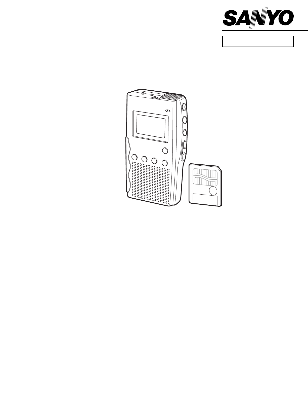
Digital Voice Recorder
ICR-B100 (XE)
Specifications
Frequency response .......... 200 Hz - 3,900 Hz (Standard mode)
200 Hz - 1,900 Hz (Long mode)
Output power ..................... 100 mW (DC max.)
Power source ..................... DC: DC 3V (“AAA” x 2)
Loudspeaker ...................... 8 ohms (1.4" Dia.)
Output terminal .................. EAR: 8 ohms (1/8" Dia.)
Dimensions ........................ Approx. 2.3" (W) x 4.4" (H) x 0.8" (D)
Weight ................................ Approx. 4 oz (104 g) (without batteries)
IMPORTANT INFORMATION
Because its products are subject to continuous improvement, SANYO
reserves the rights to modify product designs and specifications
without notice and without incurring any obligation.
PRODUCT CODE No.
164 024 01
REFERENCE No.
SM5810106
Page 2
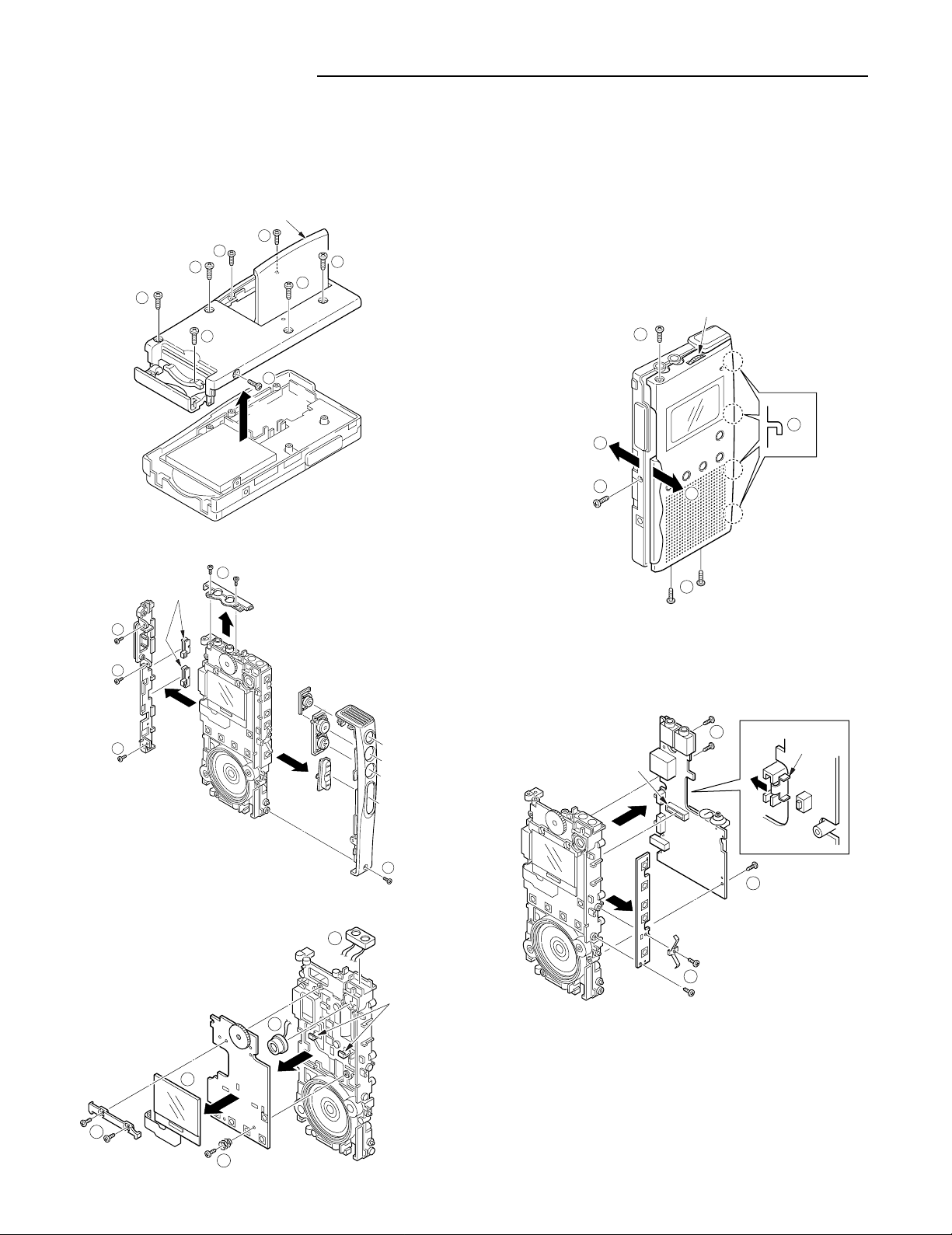
REMOVAL & INSTALLATION
· Remove the SmartMedia from the SmartMedia card compartment.
· Remove the 2 batteries and Lithium battery.
· Remove the screw or other in due order number.
· All wiring should be returned to the original position after work is completed.
1. BACK LID
BATTERY LID
2
2
1
1
1
3
3. TOP PANEL, TOP & LEFT DEC
SLIDE
KNOB
7
7
9
2. FRONT CABINET & LEFT DEC
1. Lose the left part side of a set this side.
1
1
2. Open a set from side to side
3. Because upper part volume knob hits it, do cabinet in increase
emotion a little, and open it.
VOLUME KNOB
4
HOOK
6
5
4
5
2
4. MAIN P.W.B
1. Hold base retainer while pushing back a spring plate holding a
base in check, and take it off.
2. Cross it while pushing a plate in assembly, and is crowded.
7
5. MAIN OPERATION P.W.B
14
13
15
10
CONNECTOR
8
12
11
HOOK
12
SPRING
PLATE
MAIN
P.W.B
10
- 1 -
Page 3
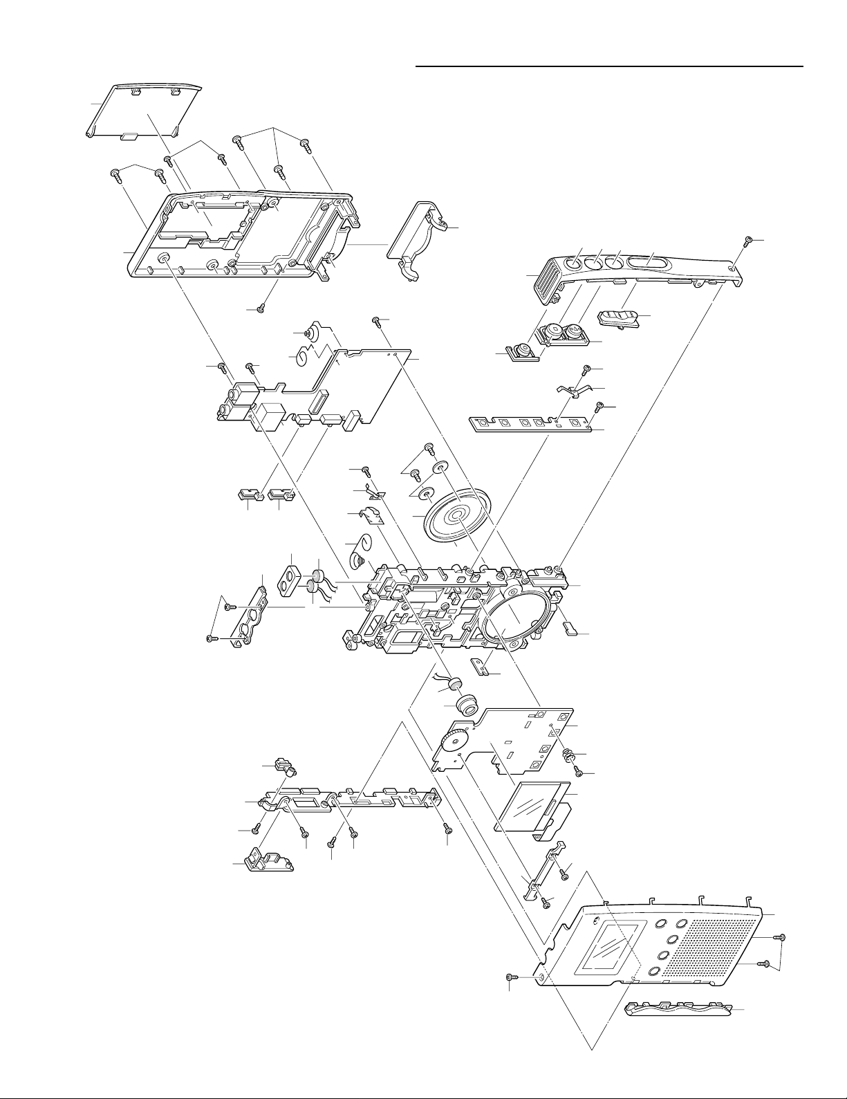
EXPLODED VIEW (CABINET & CHASSIS)
3
6
18
21
23
2
24
9
16
74
19
13
17
15
14
5
1
10
25
26
11
12
20
27
7
4
8
51
54
53
52
55
72
73
71
Y04
Y08
Y19
Y18
Y06
Y06
Y06
Y09
Y11
Y10
Y15
Y15
Y05
Y01
Y12
Y13
Y14
Y17
Y16
Y16
Y07
Y02
Y02
Y03
22
- 2 -
Page 4

PARTS LIST
PRODUCT SAFETY NOTICE
EACH PRECAUTION IN THIS MANUAL SHOULD BE FOLLOWED DURING SERVICING. COMPONENTS IDENTIFIED WITH THE IEC
!!
SYMBOL
SPECIAL SIGNIFICANCE. WHEN REPLACING A COMPONENT IDENTIFIED BY
OR PARTS WITH THE SAME RATINGS OF RESISTANCE, WATTAGE OR VOLTAGE THAT ARE DESIGNATED IN THE PARTS LIST
IN THIS MANUAL. LEAKAGE-CURRENT OR RESISTANCE MEASUREMENTS MUST BE MADE TO DETERMINE THAT EXPOSED
PARTS ARE ACCEPTABLY INSULATED FROM THE SUPPLY CIRCUIT BEFORE RETURNING THE PRODUCT TO THE CUSTOMER.
CAUTION : Regular type resistors and capacitors are not listed. To know those values, refer to the schematic diagram.
!
IN THE PARTS LIST AND THE SCHEMATIC DIAGRAM DESIGNATED COMPONENTS IN WHICH SAFETY CAN BE OF
!!
!
, USE ONLY THE REPLACEMENT PARTS DESIGNATED,
Regular type resistors are less than 1/4 W carbon type and 0 ohm chip resistors.
Regular type capacitors are less than 50 V and less than 1000 µF type of Ceramic type and Electrical type.
PACKING & ACCESSORIES
REF.NO. PART NO. DESCRIPTION
614 176 1190 INNER POLYE COVER,SET
614 301 8360 CASE,CARRY
614 301 8780 CARTON CASE,INNER
614 301 8797 INSTRUCTION MANUAL,SET
614 176 1039 INNER POLYE COVER,ACCESSORIES
645 004 4809 POLY SHEET,SET
645 034 6422 CABLE,USB
645 034 6354 BATTERY,LITHIUM 3V CR1220
645 034 7924 CARD,SSFDC 4MB
or 645 037 0724 CARD,SSFDC 4MB
or 645 026 5297 UNIT,SSFDC
645 036 5331 CABLE,AUDIO
645 038 3960 DISC,CD-ROM
614 176 2241 INNER POLY COVER, CABLE USB
645 019 1596 POLY BAG 100X300,CABLE AUDIO
CABINET & CHASSIS
REF.NO. PART NO. DESCRIPTION
1 614 301 8407 DEC,TOP
2 614 301 8414 DEC,LEFT
3 614 302 2480 DEC,GRIP
4 614 301 8452 LID,BATTERY
5 614 301 8483 PANEL,TOP
6 614 301 8254 ASSY,CABINET,FRONT
7 614 301 8469 LID,SMART,SMART,MEDIA
8 614 301 8261 ASSY,CABINET,REAR
9 614 294 4066 SPACER,MIC,FRONT,MIC
10 614 301 8490 SPACER,MIC,TOP,TOPSIDE,MIC
11 614 301 8445 KNOB,SLIDE,PLAY SP,PLAY SP
12 614 301 8438 KNOB,SLIDE,HOLD,HOLD
13 614 301 5956 SPRING,PLATE,BUTTON(BUM0800—)
14 614 301 8315 BUTTON,SKIP
15 614 301 8308 BUTTON,STOP
16 614 294 5452 MOUNTING,CB REAR
17 614 301 8292 BUTTON,REC
18 614 301 8476 MOUNTING,LCD
19 614 301 8377 CHASSIS
20 614 301 8537 TERMINAL,BATTERY,SUM-4(+)
21 614 249 0297 SPRING,COMP,SHIELD EARTH
22 614 280 0096 TERMINAL,BATTERY,SUM-4(+-)
23 614 301 8384 COVER,CONECTER,USB
24 614 301 8322 BUTTON,CUE,CUE-INDEX
25 614 301 8568 TERMINAL,LITHIUM,CR1220(-)
26 614 301 8551 TERMINAL,LITHIUM,CR1220(+)
27 614 301 8544 TERMINAL,BATTERY,SUM-4(-)
FIXING PARTS
REF.NO. PART NO. DESCRIPTION
Y01 411 030 0500 SCR TPG PAN PCS 1.7X4,DEC,TOP
Y02 411 174 8905 SCR S-TPG PAN 2X6,
CB REAR/CHASSIS
Y03 411 178 7102 SCR TPG PAN PCS 1.7X4,
CB. REAR/CHASSIS
Y04 411 178 7102 SCR TPG PAN PCS 1.7X4,
CB. FRONT/CHASSIS
Y05 411 099 0206 SCR TPG PAN PCS 1.7X5,PANEL,TOP
Y06 411 030 0500 SCR TPG PAN PCS 1.7X4,DEC,LEFT
Y07 411 175 9307 SCR PAN 1.7X2.5,
MOUNT/CB REAR/CHASSIS
Y08 411 178 7102 SCR TPG PAN PCS 1.7X4,
CB FRONT/CHASSIS
Y09 411 099 0206 SCR TPG PAN PCS 1.7X5,
CB FRONT/CHASSIS
Y11 411 030 0500 SCR TPG PAN PCS 1.7X4,CUE
Y12 411 091 9702 WASHER Z 2X8X0.5,SPEAKER
Y13 411 022 7500 SCR S-TPG PAN 2X4,SPEAKER
Y14 411 030 0500 SCR TPG PAN PCS
1.7X4,TERMINAL,LITHIUM
Y15 411 030 0500 SCR TPG PAN PCS 1.7X4,SIDE,PWB
Y16 411 030 0500 SCR TPG PAN PCS 1.7X4,
USB CONNECTOR
Y17 411 030 0500 SCR TPG PAN PCS 1.7X4,MAIN PWB
Y18 411 099 0206 SCR TPG PAN PCS
1.7X5,MOUNTIN,LCD
Y19 411 099 0206 SCR TPG PAN PCS 1.7X5,FRONT,PWB
ELECTRICAL PART
REF.NO. PART NO. DESCRIPTION
51 645 034 6415 LCD
52 645 030 0820 MICROPHONE
53 645 030 0820 MICROPHONE
54 645 030 0820 MICROPHONE
55 645 037 6061 SPEAKER,8
MAIN P.W.B ASSY
REF.NO. PART NO. DESCRIPTION
71 614 301 9459 ASSY,PWB (Only Initial)
B4401 645 034 7887 INDUCTOR,1000 OHM
B4402 645 034 7887 INDUCTOR,1000 OHM
B4403 645 034 7887 INDUCTOR,1000 OHM
B4801 645 019 1039 INDUCTOR,1000 OHM
B4802 645 019 1039 INDUCTOR,1000 OHM
B4803 645 019 1039 INDUCTOR,1000 OHM
C4002 403 296 8109 TA-SOLID 10U M 10V
C4005 403 306 6705 TA-SOLID 100U M 4V
- 3 -
Page 5

PARTS LIST
REF.NO. PART NO. DESCRIPTION
C4008 403 312 5303 TA-SOLID 47U M 6.3V
C4010 403 306 6705 TA-SOLID 100U M 4V
C4013 403 312 5303 TA-SOLID 47U M 6.3V
C4021 403 279 9109 TA-SOLID 4.7U M 10V
C4025 403 312 5303 TA-SOLID 47U M 6.3V
C4411 403 296 8109 TA-SOLID 10U M 10V
C4412 403 296 8109 TA-SOLID 10U M 10V
C4802 403 311 1603 TA-SOLID 22U M 4V
C4921 403 296 8109 TA-SOLID 10U M 10V
C4924 403 312 5303 TA-SOLID 47U M 6.3V
CN401 645 034 1588 SOCKET,DC
CN402 645 034 7610 PLUG,40P
CN403 645 033 2326 SOCKET,CARD 22P
CN404 645 034 6361 SOCKET,USB 4P
CN441 645 034 4978 JACK,PHONE D3.6
CN481 645 034 4916 JACK,PHONE D3.6
D4001 407 164 4002 DIODE RB160L-40
D4002 407 164 4002 DIODE RB160L-40
D4003 407 210 1900 DIODE 1SS400
D4004 407 130 4401 DIODE DAN202U
D4005 407 210 1900 DIODE 1SS400
D4006 407 210 1900 DIODE 1SS400
D4007 407 164 4002 DIODE RB160L-40
D4008 407 210 1900 DIODE 1SS400
D4009 407 210 1900 DIODE 1SS400
D4010 407 210 1900 DIODE 1SS400
D4011 407 210 1900 DIODE 1SS400
D4071 407 210 1900 DIODE 1SS400
D4401 407 210 1900 DIODE 1SS400
D4913 407 149 0807 DIODE 1SS355
D4914 407 149 0807 DIODE 1SS355
IC401 410 370 0805 IC UPD703017AYGC-M03-8EU
IC402 410 357 7605 IC MB89585PFV-G104-BND
IC404 409 419 8100 IC RS5C372A
IC405 410 346 5605 IC SB2020P-33372AR
IC406 409 431 3008 IC NJM2140R
IC413 409 363 5309 IC S-81233SG-QF
IC414 409 305 3103 IC TC7W74FU
L4001 645 023 2978 INDUCTOR,800 OHM
L4002 645 032 9104 INDUCTOR,22U M
L4003 645 034 8600 INDUCTOR,10U K
L4401 645 023 5818 INDUCTOR,1000 OHM
L4402 645 038 1522 INDUCTOR,10U K
L4403 645 029 7267 INDUCTOR,10U K
L4404 645 029 7267 INDUCTOR,10U K
L4405 645 029 7267 INDUCTOR,10U K
L4406 645 038 1522 INDUCTOR,10U K
L4801 645 023 2978 INDUCTOR,800 OHM
L4901 645 026 0964 INDUCTOR,10U K
L4906 645 034 8600 INDUCTOR,10U K
Q4001 405 147 7705 TR 2SK3019
Q4002 405 147 7705 TR 2SK3019
Q4003 405 147 7705 TR 2SK3019
Q4004 405 138 5703 TR DTA124EUA
Q4005 405 124 2303 TR 2SB1424-Q
or 405 124 2402 TR 2SB1424-R
Q4006 405 064 6300 TR 2SB1295-6
or 405 064 6409 TR 2SB1295-7
Q4007 405 092 4101 TR 2SC4081-R
Q4008 405 115 8703 TR DTC114TE
Q4009 405 147 7705 TR 2SK3019
Q4010 405 147 7705 TR 2SK3019
Q4011 405 137 2000 TR 2SA1576A-R
Q4012 405 133 3803 TR DTC124EUA
Q4013 405 133 3803 TR DTC124EUA
REF.NO. PART NO. DESCRIPTION
Q4014 405 129 8409 TR UMC2N
Q4015 405 133 3803 TR DTC124EUA
Q4071 405 131 2501 TR DTC114TUA
Q4401 405 137 2000 TR 2SA1576A-R
R4001 401 105 0603 MT-GLAZE 10K JA 1/16W
R4002 401 105 5509 MT-GLAZE 470K JA 1/16W
R4003 401 114 0502 MT-GLAZE 2.2M JA 1/16W
R4004 401 177 2406 MT-GLAZE 10M JA 1/16W
R4005 401 177 2406 MT-GLAZE 10M JA 1/16W
R4006 401 114 0502 MT-GLAZE 2.2M JA 1/16W
R4007 401 105 5509 MT-GLAZE 470K JA 1/16W
R4008 401 105 0702 MT-GLAZE 100K JA 1/16W
R4009 401 105 0504 MT-GLAZE 1K JA 1/16W
R4010 401 105 5509 MT-GLAZE 470K JA 1/16W
R4011 401 105 5400 MT-GLAZE 47K JA 1/16W
R4012 401 105 0603 MT-GLAZE 10K JA 1/16W
R4013 401 105 2904 MT-GLAZE 22K JA 1/16W
R4014 401 105 0504 MT-GLAZE 1K JA 1/16W
R4015 401 105 0504 MT-GLAZE 1K JA 1/16W
R4016 401 105 0504 MT-GLAZE 1K JA 1/16W
R4017 401 105 2607 MT-GLAZE 22 JA 1/16W
R4018 401 105 5301 MT-GLAZE 4.7K JA 1/16W
R4019 401 105 5301 MT-GLAZE 4.7K JA 1/16W
R4020 401 105 5905 MT-GLAZE 560 JA 1/16W
R4021 401 105 5905 MT-GLAZE 560 JA 1/16W
R4022 401 105 5905 MT-GLAZE 560 JA 1/16W
R4023 401 105 5509 MT-GLAZE 470K JA 1/16W
R4024 401 105 0603 MT-GLAZE 10K JA 1/16W
R4025 401 105 0702 MT-GLAZE 100K JA 1/16W
R4026 401 105 0702 MT-GLAZE 100K JA 1/16W
R4027 401 105 0603 MT-GLAZE 10K JA 1/16W
R4028 401 105 0702 MT-GLAZE 100K JA 1/16W
R4029 401 105 5301 MT-GLAZE 4.7K JA 1/16W
R4030 401 105 0702 MT-GLAZE 100K JA 1/16W
R4031 401 105 0702 MT-GLAZE 100K JA 1/16W
R4032 401 105 0603 MT-GLAZE 10K JA 1/16W
R4033 401 105 0702 MT-GLAZE 100K JA 1/16W
R4034 401 105 0603 MT-GLAZE 10K JA 1/16W
R4035 401 105 0702 MT-GLAZE 100K JA 1/16W
R4036 401 105 0603 MT-GLAZE 10K JA 1/16W
R4037 401 105 0702 MT-GLAZE 100K JA 1/16W
R4038 401 105 8005 MT-GLAZE 1M JA 1/16W
R4039 401 105 0702 MT-GLAZE 100K JA 1/16W
R4040 401 105 0702 MT-GLAZE 100K JA 1/16W
R4041 401 105 0702 MT-GLAZE 100K JA 1/16W
R4042 401 105 0702 MT-GLAZE 100K JA 1/16W
R4043 401 105 0504 MT-GLAZE 1K JA 1/16W
R4044 401 105 0702 MT-GLAZE 100K JA 1/16W
R4045 401 105 0504 MT-GLAZE 1K JA 1/16W
R4046 401 105 0504 MT-GLAZE 1K JA 1/16W
R4047 401 105 0504 MT-GLAZE 1K JA 1/16W
R4048 401 105 0504 MT-GLAZE 1K JA 1/16W
R4049 401 105 0504 MT-GLAZE 1K JA 1/16W
R4050 401 105 0504 MT-GLAZE 1K JA 1/16W
R4051 401 105 0504 MT-GLAZE 1K JA 1/16W
R4052 401 105 0504 MT-GLAZE 1K JA 1/16W
R4053 401 105 0504 MT-GLAZE 1K JA 1/16W
R4054 401 105 0504 MT-GLAZE 1K JA 1/16W
R4055 401 105 0504 MT-GLAZE 1K JA 1/16W
R4056 401 105 0702 MT-GLAZE 100K JA 1/16W
R4057 401 105 0702 MT-GLAZE 100K JA 1/16W
R4058 401 105 5905 MT-GLAZE 560 JA 1/16W
R4060 401 105 5301 MT-GLAZE 4.7K JA 1/16W
R4061 401 105 5905 MT-GLAZE 560 JA 1/16W
R4071 401 105 5400 MT-GLAZE 47K JA 1/16W
- 4 -
Page 6

PARTS LIST
REF.NO. PART NO. DESCRIPTION
R4072 401 105 5509 MT-GLAZE 470K JA 1/16W
R4073 401 037 5004 MT-GLAZE 0.000 ZA 1/10W
R4074 401 037 5004 MT-GLAZE 0.000 ZA 1/10W
R4075 401 037 5004 MT-GLAZE 0.000 ZA 1/10W
R4076 401 037 5004 MT-GLAZE 0.000 ZA 1/10W
R4077 401 105 7909 MT-GLAZE 0.000 ZA 1/16W
R4078 401 105 0702 MT-GLAZE 100K JA 1/16W
R4079 401 105 0504 MT-GLAZE 1K JA 1/16W
R4301 401 105 1501 MT-GLAZE 1.5K JA 1/16W
R4401 401 105 2805 MT-GLAZE 2.2K JA 1/16W
R4403 401 105 0603 MT-GLAZE 10K JA 1/16W
R4404 401 105 8203 MT-GLAZE 68K JA 1/16W
R4405 401 105 0603 MT-GLAZE 10K JA 1/16W
R4411 401 105 5400 MT-GLAZE 47K JA 1/16W
R4412 401 105 5400 MT-GLAZE 47K JA 1/16W
R4413 401 105 0504 MT-GLAZE 1K JA 1/16W
R4421 401 105 5301 MT-GLAZE 4.7K JA 1/16W
R4422 401 105 5509 MT-GLAZE 470K JA 1/16W
R4802 401 037 6506 MT-GLAZE 12 JA 1/10W
S4006 645 034 1557 SWITCH,PUSH 1P-1T
S4013 645 029 5812 SWITCH,SLIDE 1P-3T
S4014 645 018 1825 SWITCH,SLIDE 1P-2T
S4016 645 034 1564 SWITCH,PUSH 1P-1T
X4001 645 019 5082 OSC,CRYSTAL 32.768KHZ
X4002 645 034 7658 OSC,CRYSTAL 16.3840MHZ
X4071 645 026 5303 OSC,CERAMIC 6.0MHZ
FRONT CONTROL P.W.B ASSY
REF.NO. PART NO. DESCRIPTION
72 614 302 8383 ASSY,PWB,DISPLAY (Only Initial)
C5202 403 311 1603 TA-SOLID 22U M 4V
C5652 403 276 7900 TA-SOLID 2.2U M 16V
C5653 403 279 9109 TA-SOLID 4.7U M 10V
C5655 403 276 7900 TA-SOLID 2.2U M 16V
C5657 403 311 1603 TA-SOLID 22U M 4V
C5709 403 296 8109 TA-SOLID 10U M 10V
C5904 403 311 1603 TA-SOLID 22U M 4V
C5907 403 279 9109 TA-SOLID 4.7U M 10V
C5909 403 296 8109 TA-SOLID 10U M 10V
C5912 403 279 9109 TA-SOLID 4.7U M 10V
C5913 403 279 9109 TA-SOLID 4.7U M 10V
C5916 403 296 8109 TA-SOLID 10U M 10V
C5917 403 296 8109 TA-SOLID 10U M 10V
C5920 403 306 6705 TA-SOLID 100U M 4V
CN501 645 034 7634 SOCKET,40P
CN502 645 014 3472 SOCKET,FPC 12P
D5651 407 130 4500 DIODE DAP202U
D5652 407 210 1900 DIODE 1SS400
D5654 407 205 5203 DIODE RB521S-30
D5655 407 205 5203 DIODE RB521S-30
D5911 407 120 4503 DIODE DA204U
IC503 409 443 5106 IC AK4518VF
IC506 409 431 3008 IC NJM2140R
IC507 409 431 3008 IC NJM2140R
IC508 409 431 3008 IC NJM2140R
IC509 409 439 9309 IC BU4052BCFV
IC510 409 431 3008 IC NJM2140R
IC511 409 431 3008 IC NJM2140R
IC512 409 184 9609 IC NJM2073M
L5901 645 034 8600 INDUCTOR,10U K
L5902 645 026 0964 INDUCTOR,10U K
L5903 645 026 0964 INDUCTOR,10U K
REF.NO. PART NO. DESCRIPTION
L5904 645 026 0964 INDUCTOR,10U K
L5905 645 026 0964 INDUCTOR,10U K
Q5001 405 092 4101 TR 2SC4081-R
Q5301 405 131 2501 TR DTC114TUA
Q5302 405 131 2501 TR DTC114TUA
Q5501 405 131 2501 TR DTC114TUA
Q5502 405 143 9406 TR DTC323TU
Q5601 405 131 2501 TR DTC114TUA
Q5651 405 092 4101 TR 2SC4081-R
Q5652 405 092 4101 TR 2SC4081-R
Q5701 405 131 2501 TR DTC114TUA
Q5901 405 137 2000 TR 2SA1576A-R
Q5902 405 133 3803 TR DTC124EUA
Q5903 405 137 2000 TR 2SA1576A-R
Q5904 405 133 3803 TR DTC124EUA
Q5905 405 092 4101 TR 2SC4081-R
Q5906 405 064 6300 TR 2SB1295-6
or 405 064 6409 TR 2SB1295-7
R5001 401 105 2805 MT-GLAZE 2.2K JA 1/16W
R5002 401 105 0603 MT-GLAZE 10K JA 1/16W
R5017 401 105 0603 MT-GLAZE 10K JA 1/16W
R5018 401 105 2805 MT-GLAZE 2.2K JA 1/16W
R5019 401 105 4106 MT-GLAZE 3.3K JA 1/16W
R5020 401 105 5301 MT-GLAZE 4.7K JA 1/16W
R5021 401 105 0603 MT-GLAZE 10K JA 1/16W
R5022 401 105 3406 MT-GLAZE 27K JA 1/16W
R5052 401 105 0504 MT-GLAZE 1K JA 1/16W
R5059 401 105 0504 MT-GLAZE 1K JA 1/16W
R5201 401 105 2805 MT-GLAZE 2.2K JA 1/16W
R5202 401 105 0504 MT-GLAZE 1K JA 1/16W
R5203 401 105 0702 MT-GLAZE 100K JA 1/16W
R5204 401 105 0603 MT-GLAZE 10K JA 1/16W
R5205 401 105 8203 MT-GLAZE 68K JA 1/16W
R5301 401 105 2805 MT-GLAZE 2.2K JA 1/16W
R5302 401 105 1105 MT-GLAZE 12K JA 1/16W
R5303 401 105 2102 MT-GLAZE 18K JA 1/16W
R5304 401 105 0603 MT-GLAZE 10K JA 1/16W
R5305 401 105 6605 MT-GLAZE 6.8K JA 1/16W
R5306 401 105 0504 MT-GLAZE 1K JA 1/16W
R5307 401 105 2904 MT-GLAZE 22K JA 1/16W
R5308 401 105 7909 MT-GLAZE 0.000 ZA 1/16W
R5309 401 105 2904 MT-GLAZE 22K JA 1/16W
R5501 401 105 2805 MT-GLAZE 2.2K JA 1/16W
R5502 401 105 1600 MT-GLAZE 15K JA 1/16W
R5503 401 105 0702 MT-GLAZE 100K JA 1/16W
R5504 401 105 5301 MT-GLAZE 4.7K JA 1/16W
R5505 401 105 1105 MT-GLAZE 12K JA 1/16W
R5506 401 105 0504 MT-GLAZE 1K JA 1/16W
R5601 401 105 5301 MT-GLAZE 4.7K JA 1/16W
R5602 401 105 0603 MT-GLAZE 10K JA 1/16W
R5603 401 105 0504 MT-GLAZE 1K JA 1/16W
R5604 401 105 7404 MT-GLAZE 8.2K JA 1/16W
R5605 401 105 2102 MT-GLAZE 18K JA 1/16W
R5606 401 105 4601 MT-GLAZE 3.9K JA 1/16W
R5607 401 105 5301 MT-GLAZE 4.7K JA 1/16W
R5608 401 105 2904 MT-GLAZE 22K JA 1/16W
R5609 401 105 4700 MT-GLAZE 39K JA 1/16W
R5610 401 105 5202 MT-GLAZE 470 JA 1/16W
R5611 401 105 0504 MT-GLAZE 1K JA 1/16W
R5612 401 105 0504 MT-GLAZE 1K JA 1/16W
R5613 401 105 5905 MT-GLAZE 560 JA 1/16W
R5614 401 105 5905 MT-GLAZE 560 JA 1/16W
R5615 401 105 5905 MT-GLAZE 560 JA 1/16W
R5616 401 105 5905 MT-GLAZE 560 JA 1/16W
R5617 401 105 5905 MT-GLAZE 560 JA 1/16W
R5618 401 105 2904 MT-GLAZE 22K JA 1/16W
- 5 -
Page 7

PARTS LIST
REF.NO. PART NO. DESCRIPTION
R5651 401 105 0603 MT-GLAZE 10K JA 1/16W
R5652 401 105 2201 MT-GLAZE 180K JA 1/16W
R5653 401 105 0504 MT-GLAZE 1K JA 1/16W
R5654 401 105 0603 MT-GLAZE 10K JA 1/16W
R5655 401 105 2003 MT-GLAZE 1.8K JA 1/16W
R5656 401 105 0702 MT-GLAZE 100K JA 1/16W
R5657 401 105 0702 MT-GLAZE 100K JA 1/16W
R5658 401 105 0504 MT-GLAZE 1K JA 1/16W
R5701 401 105 5509 MT-GLAZE 470K JA 1/16W
R5702 401 105 8203 MT-GLAZE 68K JA 1/16W
R5703 401 105 4700 MT-GLAZE 39K JA 1/16W
R5704 401 105 4205 MT-GLAZE 33K JA 1/16W
R5705 401 105 2904 MT-GLAZE 22K JA 1/16W
R5706 401 105 0603 MT-GLAZE 10K JA 1/16W
R5707 401 105 0603 MT-GLAZE 10K JA 1/16W
R5708 401 105 0702 MT-GLAZE 100K JA 1/16W
R5709 401 105 2805 MT-GLAZE 2.2K JA 1/16W
R5710 401 105 0702 MT-GLAZE 100K JA 1/16W
R5711 401 105 1204 MT-GLAZE 120K JA 1/16W
R5712 401 105 8203 MT-GLAZE 68K JA 1/16W
R5713 401 105 4205 MT-GLAZE 33K JA 1/16W
R5801 401 099 9606 MT-GLAZE 8.2 JA 1/10W
R5901 401 105 5400 MT-GLAZE 47K JA 1/16W
R5902 401 105 5400 MT-GLAZE 47K JA 1/16W
R5903 401 105 0702 MT-GLAZE 100K JA 1/16W
R5904 401 105 5301 MT-GLAZE 4.7K JA 1/16W
R5905 401 105 0702 MT-GLAZE 100K JA 1/16W
R5906 401 105 5301 MT-GLAZE 4.7K JA 1/16W
R5907 401 105 5400 MT-GLAZE 47K JA 1/16W
R5908 401 105 5400 MT-GLAZE 47K JA 1/16W
R5909 401 105 0702 MT-GLAZE 100K JA 1/16W
R5910 401 105 5509 MT-GLAZE 470K JA 1/16W
R5911 401 105 0504 MT-GLAZE 1K JA 1/16W
R5912 401 105 0702 MT-GLAZE 100K JA 1/16W
R5913 401 098 7603 MT-GLAZE 2.2 JA 1/10W
S5001 645 018 0361 SWITCH,PUSH 1P-1T
S5002 645 018 0361 SWITCH,PUSH 1P-1T
S5003 645 018 0361 SWITCH,PUSH 1P-1T
S5004 645 018 0361 SWITCH,PUSH 1P-1T
S5005 645 018 0361 SWITCH,PUSH 1P-1T
VR501 645 034 6392 VR,ROTARY 10KBX2
CARD CONTROL P.W.B ASSY
REF.NO. PART NO. DESCRIPTION
73 614 302 8390 ASSY,PWB,SW (Only Initial)
R6001 401 105 2805 MT-GLAZE 2.2K JA 1/16W
R6002 401 105 4106 MT-GLAZE 3.3K JA 1/16W
R6003 401 105 5301 MT-GLAZE 4.7K JA 1/16W
R6004 401 105 0603 MT-GLAZE 10K JA 1/16W
S6001 645 018 0361 SWITCH,PUSH 1P-1T
S6002 645 018 0361 SWITCH,PUSH 1P-1T
S6003 645 018 0361 SWITCH,PUSH 1P-1T
S6004 645 018 0361 SWITCH,PUSH 1P-1T
S6005 645 018 0361 SWITCH,PUSH 1P-1T
LID SWITCH P.W.B ASSY
REF.NO. PART NO. DESCRIPTION
74 614 303 9419 ASSY,PWB,SW2 (Only Initial)
S7001 645 035 5912 SWITCH,PUSH 1P-1T
- 6 -
Page 8
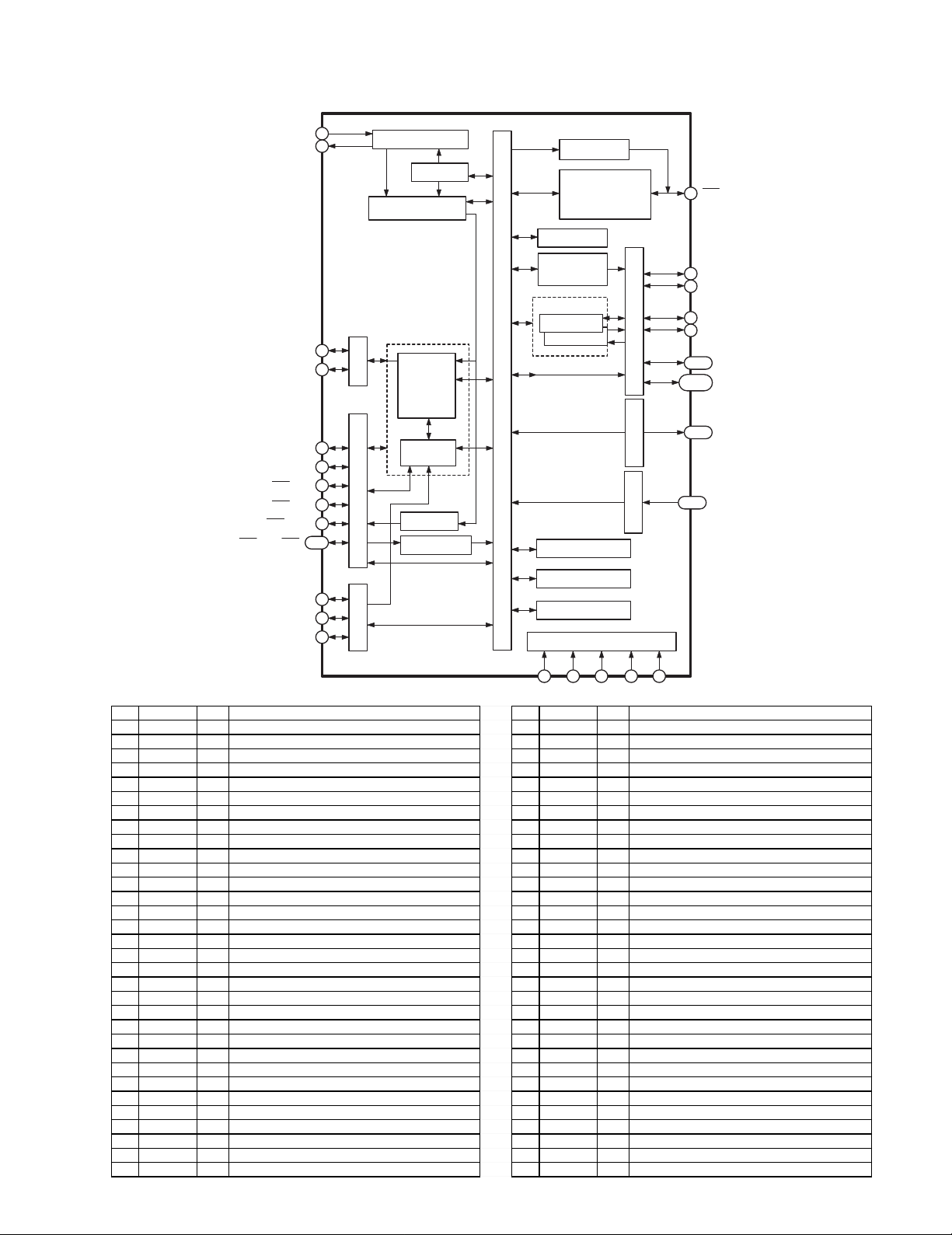
IC BLOCK DIAGRAM
The figure which isn't mentioned please watch a schematic diagram.
IC401 UPD703017 (MICRO COMPUTER)
No. Pin Name I/O Function No. Pin Name I/O Function
1 LCD DATA I/O LCD Driver IC data output 51 I O4 I/O Smart media (input/output data)
2 LCD CLK I/O LCD Driver IC clock output 52 I O5 I/O Smart media (input/output data)
3 P CO N O Power control (Power ON=high) 53 I O6 I/O Smart media (input/output data)
4 A MUTE1 O Audio mute (Mute=high) 54 I O7 I/O Smart media (input/output data)
5 A MUTE2 O Audio mute (Mute=high) 55 BVDD
6 VDD O Power supply 56 BVSS
7 VSS O GND 57 USB ON I USB ON/OFF check (ON=High)
8 DAC PWR O DAC Power control (Power OFF=LOW) 58 AC IN I AC Adapter detect (AC have=LOW)
9 DD PWR O DD Converter power control (Power ON=high) 59 MIC IN I Detect the external mic presence (There is a Mic=LOW)
10 PULL UP O PULL UP Resister power control (Power ON=high) 60 SSFDC SW I SmartMedia insert switch
11 AMP PWR O AMP Circuit power control (Power ON=high) 61 SSFDC IN I Detect the SmartMedia presence (Yes=LOW)
12 MCLK IN I MCLK Count input 62 SSFDC 3V I Detect the 3.3V SmartMedia (3.3V=High)
13 ADC POW O ADC Power control (Power OFF=LOW) 63 SSFDC REC I Check write on a SmartMedia (Ability=High)
14 ADC CLK O A/D,D/A Converter master lock output 64 R/B I/ O
15 DAC LRCK I/O ADC/DAC LRCK output 65 MIC SEL1 O Mic change control
16 BEEP O Beap signal output 66 MIC SEL 2 O Mic change control
17 LCD RESET I/O LCD Controller Reset output 67 MIC SEL 3 O Mic change control
18 IC/VPP General action =LOW/FLASH time = high 68 MIC SENS1 O Mic sensitivity control (1)
19 USB 0 I/O Data input/output 69 MIC SENS2 O Mic sensitivity control (2)
20 USB 1 I/O Data input/output 70 SEL 24H I Select the 12H/24H change (12H=LOW)
21 USB 2 I/O Data input/output 71 AVDD
22 USB 3 I/O Data input/output 72 AVSS
23 USB 4 I/O Data input/output 73 AVREF
24 USB 5 I/O Data input/output 74 KEY0 I Key input
25 USB 6 I/O Data input/output 75 KEY1 I Key input
26 USB 7 I/O Data input/output 76 FOOT IN I FOOT SW input
27 USB WR O Data lead select (Lead=LOW) 77 BATT IN I Battery residual quantity check
28 USB RD O Data lead select (Lead=LOW) 78 HOLD SW I Hold SW input
29 USB STP I Device detector (Permission=HIGH) 79 FAST SW I High speed listening (ON=LOW)
30 USB CE O Chip enable (Enable=LOW) 80 SLOW SW I Low speed listening (ON=LOW)
31 RESET I Reset signal 81 VAS IN I Sound signal level detect
32 XT1 I 82 LEVEL IN I Volume/VAS sensitivity level input
33 XT2 83 I
34 VDD 84 CASE SW I Ba tt er y li d d et e ct sw i tc h
35 X2 Main oscillation (Ceramic 16.384 MHz) 85 I
36 X1 I Main oscillation (Ceramic 16.384 MHz) 86 O
37 VSS GND 87 O
38 CLKOUT 88 USB STOP O
39 I/O 89 O
40 WPB O Write protect 90 ENROL I Enrol output permission (Permission=LOW)
41 R/B I Ready/Busy check (Busy=low) 91 O
42 WEB O Write enable 92 O
43 REB O Lead enable 93 LCD CS I/O LCD Driver IC chip select output
44 CEB O Chip enable 94 RTC DATA I/O Real time clock IC data output
45 ALE O Address ratch 95 LCD RS I/O LCD Driver IC resister select output
46 CLE O Command ratch 96 RTC CLK I/O Real time clock IC clock output
47 I O0 I /O Smart media (input/output data) 97 DAC IN I ADC serial data input
48 I O1 I /O Smart media (input/output data) 98 DAC OUT O DAC serial data output
49 I O2 I /O Smart media (input/output data) 99 DAC CLK O ADC/DAC clock output
50 I O3 I /O Smart media (input/output data) 100 O
- 7 -
Page 9
IC BLOCK DIAGRAM
IC402 MB89585 (MICRO CONTROLLERS)
22
X0
23
X1
Main Clock Oscillator
Clock Control
PLL Circuit
Circuit
Reset Output
Power ON Reset
circuit
(Watch dog timer)
21bit Time
Baseter
RST
19
RPVP
RPVM
P51/R
P50/OBH/IBF/W
P36/INT6/WEX
P37/INT7/RDX
P30/INT0/RCLK
P31/INT1~P35/INT5
P52/EFX
P53/FFX
P54/CEX
6~10
8bit PWM Timer
rt
a
P
UART
51
52
USB DRV
15
rt
13
o
P
11
I/O
S
12
O
M
C
5
16
17
18
Noh I/O Port
USB
Function
Circuit
DMA
Clock Output
External
Interrupt (Level)
Internal Path
SIO
RAM 1k/512 Byte
F2MC - 8L CPU
ROM 8k/16k Byte
Other T erminal
24
49
Vss
Vcc
MOD0 MOD1 C
I/O
S
O
M
C
CMOS Out Part
CMOS In Part
21
20
50
P46/PWM1/U1/D6
3
4
P47/PWM2/D7
1
P44/UCK/D4
2
P45/U0/D5
61~64
P40/D0~43/D3
48~41,
P00~07,P10~17
40~33
32~25
P20~27
P60/D10~P67/D17
53~60
No. Pin name I/O Funtion No. Pin name I/O Funtion
1 USB4 I/O Data (to main cpu) 33 O
2 USB5 I/O Data (to main cpu) 34 O
3 USB6 I/O Data (to main cpu) 35 O
4 USB6 I/O Data (to main cpu) 36 O
5 O Open (low output) 37 O
6 O Open (low output) 38 O
7 O Open (low output) 39 O
8 O Open (low output) 40 O
9 USB ON O USB connection state output (connection=High) 41 O
10 O Open (low output) 42 O
11 USB WR I Data write signal input 43 O
12 USB RD I Data read signal input 44 O
13 USB STP O State output 45 O
14 VSS GND. 46 O
15 P CON O Power control (ON=High) 47 O
16 MANUAL I Suspected data transmission mode (Suspected=Low) 48 O
17 O Open (low output) 49 VCC Power supply (3.3V)
18 USB CE O Chip enable input 50 C Connect 0.1uF
19 RESET I Reset signal 51 USB+ I/O USB Connect port
20 MOD0 I GND (Memory access setting terminal) 52 USB- I/O USB Connect port
21 MOD1 I GND (Memory access setting terminal) 53 I GND Connect
22 X0 Main oscillation (6MHz) 54 I GND Connect
23 X1 Main oscillation (6MHz) 55 I GND Connect
24 VSS GND 56 I GND Connect
25 OUT7 O Open (low output) 57 I GND Connect
26 OUT6 O Open (low output) 58 I GND Connect
27 OUT5 O Open (low output) 59 I GND Connect
28 OUT4 O Open (low output) 60 I GND Connect
29 OUT3 O Open (low output) 61 USB0 I/O Data (to main cpu)
30 OUT2 O Open (low output) 62 USB1 I/O Data (to main cpu)
31 OUT1 O Open (low output) 63 USB2 I/O Data (to main cpu)
32 OUT0 O Open (low output) 64 USB3 I/O Data (to main cpu)
- 8 -
Page 10
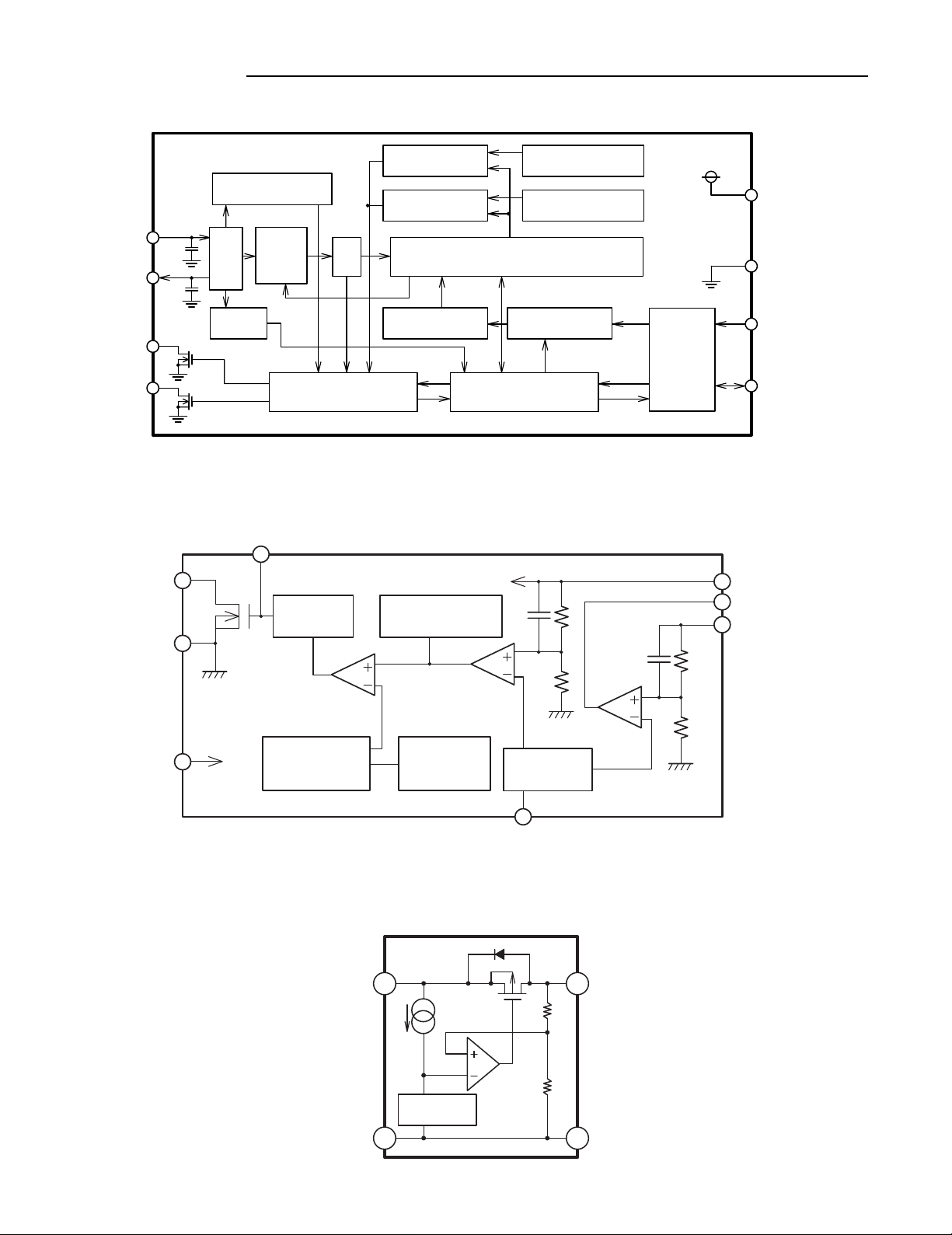
IC BLOCK DIAGRAM
IC404 RS5C372A (CMOS Real Time Clock)
COMPARATOR_A
32kHz OUTPUT
OSCIN
OSCOUT
/INTRA
/INTRB
CONTROL
7
6
5
1
OSC
OSC
DETECT
DIVIDER
CORREC
-TION
INTERRUPT CONTROL
DIV
COMPARATOR_B
(SEC,MIN,HOUR,WEEK,MONTH,YEAR)
ADDRESS
DECODER
TIME COUNTER
SHIFT REGISTER
IC405 SB2020P (Ascent and Descent type DC-DC Convertor)
SWR_EXT
7
8
Lx
GND
Buffer,
Driver
1
Noh MOS
SW
PWM
Comparator
Internal VDD
Phase
Compensation
SWR
Error Amp.
ALARM_A REGISTER
(WEEK,MIN,HOUR)
ALARM_B REGISTER
(WEEK,MIN,HOUR)
ADDRESS
REGISTER
VR
Error Amp.
I/O
CONTROL
5
VUP
3
VR_EXT
2
VOUT
8
V
DD
4
V
SS
2
SCL
SDA
3
CE
6
Ramp Wave
Generator,
OSC
IC413 S-81233GS (Voltage Regulator)
V
GND
IN
PWM/PFM
Dual Mode
Controller
2
REFERENCE
VOLTAGE
1
- 9 -
Vret with
Soft Start
4
CSS
3
V
OUT
NC
Page 11

IC BLOCK DIAGRAM
IC414 TC7W74FU (D-type Flip Flop with Preset and Clear)
CK
Q
GND
1
2
D
3
4
8
7
6
5
VCC
PR
CLR
Q
Truth Value
INPUTS OUTPUTS
CLR PR D CK Q Q
L H X X L H CLEAR
H L X X H L PRESET
L L X X H H ----H H L L H ----H H H H L ----H H X Qn Qn NO CHANGE
FUNCTION
IC503 AK4518VF (Regulater 16bit A/D, D/A Converter)
AINL
VCML
AINR
VCMR
VRAD
VRDA
VCOM
AOUTL
AOUTR
VA AGND
24
22
6
5
3
4
2
1
21
19
20
Modulator
Modulator
LPF
LPF
PWAD
ΔΣ
ΔΣ
7
Common Voltage
ΔΣ
Modulator
ΔΣ
Modulator
8
PWDA
23
DGNDVB
VD
14
Decimation
Decimation
13
Filter
Filter
8x
Interpolator
8x
Interpolator
Clock
Divider
Serial I/O
Interface
DEM0 DEM1
9
MCLK
16
CMODE
10
LRCK
11
SCLK
12
SDTO
15
SDTI
1718
IC509 BU4052 (Analog Multiplexers/Demultiplexers)
VDD
16
OUT
12
14
15
11
IN
C
OUT
IN
C
OUT
IN
C
OUT
IN
C
0X
1X
2X
3X
No. Pin name I/O Function
1 VRDA I Voltage Reference Input Pin for DAC,VA
2 VRAD I Voltage Reference Input Pin for ADC,VA
3 AINR I R-ch Analog Input Pin
4 VCMR O R-ch Common Voltage Output Pin 0.45 x VA
5 VCML O L-ch Common Voltage Output Pin 0.45 x VA
6 AINL I L-ch Analog Input Pin
7 PWAD I ADC Power Down Mode Pin "L" : Power down
8 PWDA I DAC Power Down Mode Pin "L" : Power down
9 MCLK I Master Clock Input Pin
10 LRCK I Input/Output Channel Clock Pin
11 SCLK I Audio Serial Data Clock Pin
12 SDTO O Audio Serial Data Output Pin
13 DGND --- Digital Ground Pin
14 VD --- Digital Power Supply Pin
15 SDTI I Audio Serial Data Input Pin
16 CMODE I Master Clock Select Pin "H" :384fs or 512fs, "L" : 256fs
17 DEM1 I De-emphasis Frequency Select Pin
18 DEM0 I De-emphasis Frequency Select Pin
19 AOUTL O L-ch Analog Output Pin
20 AOUTR O R-ch Analog Output Pin
21 VCOM O Common Voltage Output Pin, 0.45 x VA
22 AGND --- Analog Ground Pin
23 VB --- Substrate Pin
24 VA --- Analog Power Supply Pin
X-COMMON
13
Truth Value
A
10
9
B
INHIBIT A B ON SWITCH
L L L X0 Y0
L H L X1 Y1
L L H X2 Y2
0Y
1Y
2Y
3Y
OUT
IN
1
5
2
4
C
OUT
IN
C
OUT
IN
C
OUT
IN
C
LOGIC LEVEL CONVERTER
INH
6
Y-COMMON
3
L H H X3 Y3
H X X NONE
87
VEE
VSS
- 10 -
Page 12

LCD DISPLAY
M3
L1
L2
L3
L4
L5
M2
M1
DI3
DO3
DO2 DO1 V1
DI2 DI1 V2
B1
L6
L7
L8
M5
M6
M4
DO4
DI4
DO5
No.
1
2
3
4
5
6
7
8
9
10
11
12
Symbol
Reset
V1
V2
CICI+
VEE
VSS
VDD
SCL
SDA
RS
CS
SEG3
SEG4
SEG5
SEG8
SEG9
SEG10
SEG13
SEG14
SEG15
SEG18
SEG19
V1
SAVE
B3
B4
B2
B1
1
R
V2
BASS
INTRO
ST
SEG23
SEG24
SEG25
SEG28
SEG29
SEG30
SEG33
SEG34
SEG35
SEG39
SEG40
DO4
DO3
DO2
DO1
DO8
DO7
DO6
DO5
AM
MARK
SYNC
DI4
DI3
DI2
DI1
DI8
DI7
DI6
DI5
PM
TOTAL
DO8DO7 DI8DI7DI6DO6DI5
SEG44
SEG45
SEG48
SEG49
SEG50
SEG53
SEG54
SEG55
SEG58
SEG59
SEG60
T IME
AUTO
M6
M5
M4
M3
M2
M1
B2
B3
B4
P COM17P COM17P COMOP COM17P COMO P COMO
DATE
REC
L8
L7
L6
L5
L4
L3
L2
L1
INPUTTERMINAL
SEG20
VAS
MONO
ANODE&GRIDASSIGNMENT
- 11 -
Page 13

SCHEMATIC DIAGRAM
This is a basic schematic diagram
- 13 -- 12 -
PRODUCT SAFETY
NOTICE
Each precaution in this manual
should be followed during
servicing. Components
identified with the IEC symbol
in the parts list and the
!!
!
schematic diagram designated
components in which safety can
be of special significance. When
replacing a component identified
!!
!
, use only the replacement
by
parts designated, or parts with
the same ratings of resistance,
wattage or voltage that are
designated in the parts list in this
manual. Leakage-current or
resistance measurements must
be made to determine that
exposed parts are acceptably
insulated from the supply circuit
before returning the product to
the customer.
Page 14

WIRING DIAGRAM (PARTS SIDE VIEW)
FRONT CONTROL
P.W.B
WIDE
MC501
NARROW
MC502
CANCEL
MC503
CARD
CONTROL
P.E.B
BATTERY
DC 3V
BACK UP
BATTERY
DC 1.5V
LID
SWITCH
P.W.B
MAIN P.W.B
SP401
SPEAKER
GY WH
- 15 -- 14 -
Page 15

WIRING DIAGRAM (PATTERN SIDE VIEW)
CARD
CONTROL
P.W.B
FRONT CONTROL P.W.B
MAIN P.W.B
LID
SWITCH
P.W.B
- 16 -
Mar. / '00 / 1200 BB Printed in Japan
SANYO Technosound Co., Ltd.
Osaka, Japan
 Loading...