

Page 1
..
Service Manual
...
I FILE NO.
I
CD Changer stereo
Music System
GCD 2700 (AU)
I II
~
.Illaoa
II
LE=4E!l
Hww-M El
-..
CONTENTS
SPECIFICATIONS . . . . . . . ..’...... ..’ . . . . . 1
LASER BEAM INFORMATION . . . . . . . . . . . . . 1
OPERATING THE RESET SWITCH . . . . . . . . . 2
COOPERATION . . . . . . . . . . . . . . . . . . . . . . . 2
REMOVAL AND INSTALLATION . . . . . . . . . . . 5
TUNER ADJUSTMENTS . . . . . . . . . . . . . . . . . 7
TAPE DECK ADJUSTMENTS . . . . . . . . . . . . . 9
ILLUSTRATION OF CD CHANGER MOVEMENT 12
CD PLAYER’S SERVICE MODE . . . . . . . . . . . . 15
ADJUSTMENTS . . . . . . . . . . . . . 19
\
‘.
.-. --- -
------,
PRODUCT CODE No.
129 390 02
EXPLODEDVIEW . . . . . . . . . . . . . . . . ...’... 23
PARTS LIST . . . . . . . . . . . . . . . . . . . . . . . . . . 26
INTERCONNECT DIAGRAM . . . . . . . . . . . . . . 37
IC BLOCK DIAGRAM . . . . . . . . . . . . . . . . . . . 38
LCD DESCRIPTION . . . . . . . . . . . . . . . . . . . . 41
SCHEMATIC DIAGRAM . . . . . . . . . . . . . . . . . . 42
WIRING DIAGRAM . . . . . . . . . . . . . . . . . . . . . 44
IC DESCRIPTION . . . . . . . . . . . . . . . . . . . . . . 52
lC& TRANSISTOR VOLTAGES . . . . . . . . . . . . 70
REFERENCE No. SM 580050
I
Page 2

ii
.-
;PECIFICATIONS
AMPLIFIER SECTION
Output po+vec
12 Watts/ch (10% THD)
Input sensitivii and impedance VIDEO 300 mV/50 kohms
Graphic equafizer control:
~ 6 d6 (100
Hz, 1 kt-fz. 10 kHz)
Bass expandez
+ 8 de
(lm Hz)
TUNER SECTION
(FM)
Frequency range
87.5 MHz -106.0 MHz (50 kHz eteps)
Usable sensitivity
20.7 d13f (mono)
(AM)
Frequency range
531 kHz -1,701 kHz (9 kHz steps)
Sensitivity:
800 pV/m (AM Loop antenna)
CASSEITE DECK SECTtON
Track system: 4-track, 2-channel stereo
Frequency response
60
t-fz-13 kHz (Cr02)
Signal to noise ratkx
50 dB/56 dB (DOLBY NR OFF/ON)
Wow and fluttec
0.15 % (WRMS)
Tape speed:
4.75 cm/sec
Fast fomard and Rewind time
Approx. 110 sec. (C-60)
CD PtAYER SECTfON
Channels
2-cham’tel stereo
Sampling freque~
441 kHz
Digital filtec
8x0
varsarnpfing
D/A conversion:
Dual 16-hi finear D/A
converters
Pick-up
Optical 3-beam semiconductor laser
Frequency response
20 Hz -20 kHz
Total harmonic distortiorx
0.04% (1 kHz)
Signal to noise ratio
96 dB
Wow and fluttec
Below measurable limits
GENERAL
Power requirements
AC 230-240 V. 50
Hz
Power consumption
sow
Dimensions (W x H x D):
Approx 360x353x399 mm
Weight
APpnJx. 8.2 kg
,, —
. . ... .-
RB-2000 WffRELESS REMOTE CONTROL
Power requirements:
2 “SUM-3/AWRLT’ batteries
Dimensions (W x H x D): Approx.41 x 175x 18mm
Weight
Approx. 63 g (without batteries)
.“ :.
,,
:.’ ..,,.,
.,
IMPORTANT INFORMATION
Because its products are subject to continuous improvement, SANYO reserves the right to modify producf designs and
specifications without notice and without incurring any obligation.
LASER BEAM INFORMATION -
...-. —
.“
:...,
.....
(1) A pick-up that emits a laser beam is used in this compact disc player.
CAUTION - USE OF CONTROLS OR ADJUSTMENTS OR
PERFORMANCE
OF PROCEDURES OTHER
THAN THOSE SPECIFIED HEREIN MAY
RESULT IN HAZARDOUS RADIATION
EXPOSURE.
LASER OUTPUT ...........0.6 mW Max.
DANGER - Invisible laser radiation when open.
AVOID DIRECT EXPOSURE TO BEAM.
I
I 11= EH-Em-=
m
-1-
‘L-1
—
-s
if
“.“.
;----
_.&
. .
Page 3
i
.+
#
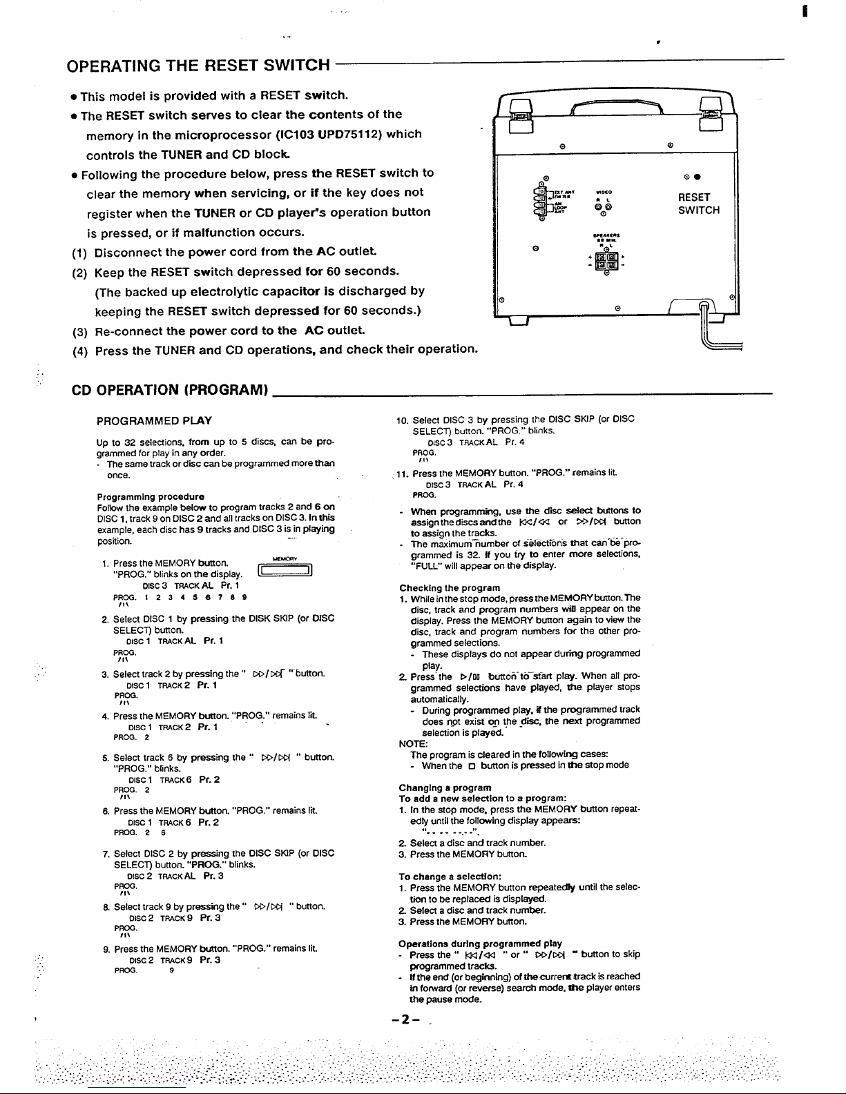
OPERATING THE RESET SWITCH
● This model is provided with a RESET switch.
● The RESET switch serves to clear the contents of the
memory in the microprocessor (IC103 UPD75112) which
controls the TUNER and CD block.
● Following the procedure below, press the RESET switch to
clear the memory when servicing, or if the key does not
register when the TUNER or CD playe~s operation button
is pressed, or if malfunction occurs.
(1)
(2)
(3)
(4)
Disconnect the power cord from the AC outlet.
Keep the RESET switch depressed for 60 seconds.
(The backed up electrolytic capacitor is discharged by
keeping the RESET switch depressed for 60 seconds.)
Re-connect the power cord to the AC outlet.
Press the TUNER and CD operations, and check their operation.
RESET
SWITCH
—
111—
CD OPERATION (PROGRAM)
....
..
PROGRAMMED PLAY
Up to 32 selections, from up to 5 discs, can be programmed for play in any order.
The same track or disc can be programmed more then
once.
Programming procedure
Follow the example below to program tracks 2 and 6 on
DISC 1, track 9 on DISC 2 and all tracks on DISC 3. in thii
example, each disc has 9 tracks and DISC 3 is in playing
position.
-..
1. Press the MEMORY button.
“’PROG.” blinks on the display.
*
Disc 3 TRAcKAL i%. 1
P~~1234S 6789
2. Select DISC 1 by
pressingthe DISK SKiP (or DISC
SELECT button.
OISC1 TMCK AL Pr. 1
PROG.
/1!
3. Select track 2 by pressing the” DD/ti ““button.
OISC1
TRACK 2 Pr. 1
PROG.
/!!
4. Press the MEMORY button. “’PROG.” remains fit.
OISC1 TPACK2 pr. i
PROG. 2
5. Select track 6 by pressing the “ DO/M2 0’button.
“PROG.” blinks.
OISC1
TRACK 6 Pr. 2
PROO. 2
11!
6. Press the MEMORY button. “PROG.” remains lit.
DISC1 TRACK6 Pr. 2
PROG. 2 6
7. Select DISC 2 by pressing the DISC SKIP (or DISC
SELECT) button. “PROG.” blinks.
DISC2
TPACK AL Pr. 3
P~~.
6. Select track 9 by pressing the” CO/cci “’button.
DISC2
TRACK 9 pr. 3
PROG.
Ilt
9. Press the MEMORY button. “PROG.” remains lit.
DISC2 TRACK9 Pr. 3
PROG.
9
10. Select DISC 3 by pressing the DISC SKIP (or DISC
SELECT) button. “’PROG.” blinks.
OISC3 TRACKAL P;. 4
PROG.
18$
.11. Press the MEMOFtY button. ““PROG.” remains lit.
Disc 3 TPACKAL
Pr. 4
PRCG.
When programming, use the disc aefect buttons to
assign the discs end the K</~ or >>/CCi button
to assign the tracks.
The maximurn%umber of selections that ceh-t%-pr~
grammed is 32. ff you try to enter more selections,
“’FULL” will appear on the display.
Checking the program
1. While in the stop mode, press the MEMORY button. The
disc, track and program numbers wiff appear on the
display. Press the MEMORY button again to view the
disc, track and program numbers for the other programmed selections.
These displays do not appear during programmed
play.
2 Press-the D/oo button” to--at-m Pkw. when all Pro-
grammed selections have played, the player stops
automatically.
During programmed play. if the programmed track
does not exist ofl \he -d=, the next programmed
selection is played.
NOTf3
The program is cleared in the following cases
When the ❑ button is pressed in the stop mode
Changing a program
To add a new aelectlon to a program:
1. In the stop mode. press the MEMORY butron repeatedly until the following display appears
“’-- . . . ....”.
2. Select a disc and track number.
3. Press the MEMORY button.
To change a selection:
1. Press the MEMORY button repeatedly until the selec-
tion to be replaced is displayed.
2. Select a disc and track number.
3. Prass the MEMORY bulton.
Operation during programmed play
- Press the “ M lad “ or” WIDC4 - button to S~P
programmed tracks.
If the end (or beginning) of the currera srack is reached
in forward (or reverse) search mode, @w player enters
the pause mode.
-2- .
Page 4
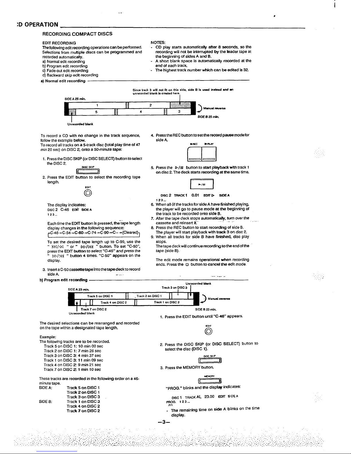
:D OPERATION ●
RECORDING COMPACT DISCS
EDIT RECORDING
NOTES
The following edfi recording operations can be performed.
- CD play starts automatically after 8 seconds, so the
Selections from muftiple discs can be programmed and
recording will not be interrup@d by the feader tape at
recorded automatically.
the beginning Ofsides A and B.
a) Normal edit recording
A short blank space is automatically recorded at the
b) Program edit recording
end of each track.
c) Fade-our edit recording - The highest track number wfriih can be ediied is 32.
d) Backward skip adii recording
s) Normal edit recording
Since track 3 will not rc on rhis side, site e is used inat&xk and M
umecorded blank is cfealed here.
To record a CD with no change in the track sequence,
follow the example befow.
To record all tracks on a S-track disc (total play time of 47
min 20 see) on DISC 2, onto a 50-minute tape:
1. Press the DISC SKfP (or DISC SELECT) button to select
the DISC 2.
lrlsc
SKIP
~
2. Press the EDIT button to select the recording tape
length.
EOIT
o
The display indicates
DISC2 C416
Eti S105 A
123...
..
Each time the EDIT button is pressed, the tape length
display changes in
me following sequence
#246 --C-54 -C@3--74 -C-90=- -(Cleared)l
To set the desired tape length up to C-99, use the
“ kM/c4 ‘“ or “ wlrxi “ button.
To set “C-5W,
press the EDIT button to sefect “CJ$6’. and press the
“’ COIN
“ button 4 times. “C-W” appears on the
display.
3. Insert a C-SOcaasettetapeinto thetapedeckto record
side A.
-. ..
4.
5.
6.
7.
8.
9.
Press the REC buttonto set the racordpause mode for
s“tie A.
● REC >RAv
Cn
——
Press the Plm button to start playback with track 1
on dtsc 2.
me deck starts recording at me sametime.
DISC2 TR4CK 1 0.01 EOITb SIOEA
123...
When all 6f the tracks for side A have finished playing,
the player will go to pause mode at the beginning of
the track to be recorded onto side B.
After the tape deck stops aufomadceffy, turn wer the
cassette and reinsen it-
-----
Press the REC button to start recording of side B.
The player will start playback with track 3 on disc 2.
When all tracks for side B have finished, disc play
stops.
The tape
deck will continue recording tome end ofthe
tape (side B).
The edit mode remains operational when recording
ends. Press the o button to cancef the edii
mode
--- .. . -
b) Program edit recordfrkg
Unrecorded blank
SlCEA23min.
Track 3 on DISC 3
Track 5 on DISC
1
II
-
Track 2 on DISC 1
II ‘ I
#i
I
1]
[1
‘,3
Mmud
r—
Track 4 on OISC 2
Track 1 on OfSC 3
[ Tr&k 7 on DISC 2 SIDE 823 min.
Unre&ded blank
1. Press the EDIT button until ““C-4& appears.
The desired selections can be rearranged and recorded
on the tape within a designated tape length.
EO,l
Q
Examde:
The f~llowing tracks are to be recorded.
Track 5 on DISC 1:10 min 00 sec
Track 2 on DISC 1:7 min 26 sec
2. Press the DISC SKIP (or DISC SELECT) button to
sefect the disc
(DISC1).
Track 3 on DISC 34 min 37 sec
Usc
YaP
Track 1 on DISC 3:11 min 09 sec
~
Track 4 on DISC 2:9 min 21 sec
Track 7 on DISC 21 min 10 sec
3. Press the MEMORY button.
These tracks are recorded in the following order on a 46-
minute tape.
SIDE A
Track 5 on DISC 1
Track 2 on DISC 1
Track 3 on DISC 3
SIDE B: Track 1 on DISC 3
Track 4 on DISC 2
Track 7 on DISC 2
Ie5
“PROG.” btinks and the dispfay indicates:
DISC 1 TR4CKAL 23.00 EOIT SIDEA
P:~
123...
The remaining time on side A blinks on the time
display.
-3–
,.
Page 5

.-
9
CD
......
............. . .
OPERATION
4. press the w/@ or w/~ b~on to select the tfacfr 7. Repeat steps 2-5 to program the tracks to be re(lRACK 5). ~~ XM
~
corded onto side B.
“PROG.” remains Iii. If a track exceeding the remaining time on side B is
OISC i TRAcK 5 13.00 EO~ s05 A programmed, “Err’” wiii appear in the display for 4
PROQ. 1 23 ...
seconds.
S. Press the MEMORY button. 8. Insert the C-46 cassette tape into the tape
deck to
[=1
record side A
9. Press the REC button. ‘=CC
b
RAY
I 1
‘“PROG.O’remains lit.
DISC 1 TRACK 5 13.00 EOIT SIDE A
LL.1
PROO. 5
10. Press the Dim bunon. Recording starts.
6. Repeat steps 2-5 to program the tracks to be
re-
cmded onto side A
m
Ifa track which exceeds the remaining time oneide
A is selected, its remaining time bfinks on the d@
The programmed tracks will play in sequence starting
from track 5 on cksc 1, and pause at the end of track 3
on disc 3.
play.
When the MEMORY button is pressed, “SIDE A“
DISC 1 TRACK5 0.01 EOITD
SIOEA
disappears and “SIDE B“ appears. The rem-g
PROO. 25
time Dn side B appears on the display. Thii and
subsequent tracks are recorded on side B.
11. Follow steps “W’ to”1 O of ‘“Normal edit recording”.
C) Fade-ouf edff recording
The sound is automatjcaffy faded out at the
end ofsides A
end B, according to the selected tape len@’t.
Fade out (10 see.)
SIOE A so min.
.-.
1
II
2
II
3
II
4
II
s
11
a
II II II
11
>
Manual reverse
11
10
a
a
7
e
I
Fade our (10 sec.)
Example
To record onto a 60-minute tape
1.
2
3.
4.
5.
d)
1.
2
3.
4.
Press the EDfT button un~l “C-W’ appears on the
display.
Press the FADE button.
-.,
‘“FADE” appears.
Insert a C-60 cassene tape into the tape deck to record
side A.
(If you desire, program the tracks. Refer to PRO-
GRAMMED PLAV on page 10)
Press the REC button.
Press the D/oo bunon. Recording starts.
The pfayerwill start playback with track 1 onsideAand
proceed in sequence until track 6 is recordecL The
display indicates:
OISC 1 TRACK 1 FADE 0.01 EOIT D SIDE A
123...
. . ... .
Record from the beginning of a track. SIOE B 30 min.
6.
Follow steps “’6 to ‘“1W of “’Normal ed~ recording”.
“’FADE blinks as the sound fades out (1O seconds).
When the remaining tape length is lass than 10 sec.,
the track, curreryJ playing is not faded out.
. _.. _ ._
The sound isalso faded out when a track is interrupted
... .. .
at the end of side B.
.
Backward skip edit recording
Track 4 will be interrupted.
. .
S1OEA -1 -’
1
!1
2
II
3114
811711 6
II
5
II
4
~>
Manual rewerse
SIOE B f
Record from the beginning of a track.
Track a will be interrupted
Press the EDtT button until “C-”
appears cm the
display.
Press the REC button.
Press the b/Oo button.
Recording starts on side A with track 1.
Follow steps “6’ to “9’ of “Normal edit recorder@-.
MANUAL RECORDING
1.
2.
,..,.:..
.. . ..:”,
... . .. .
For programmed recording, program the matssi@f in
advance (as described under “PROGRAMMED PtXY’).
Press the REC button.
Press the D/oo bunon. Recording starts.
If-the FADE button is pressed during racordinf& the
sound begins to fade out irom that point (abm9t 10
seconds). The CD player pauses, but the
deck @rntin-
ues recording.
–4–
Page 6
..
v
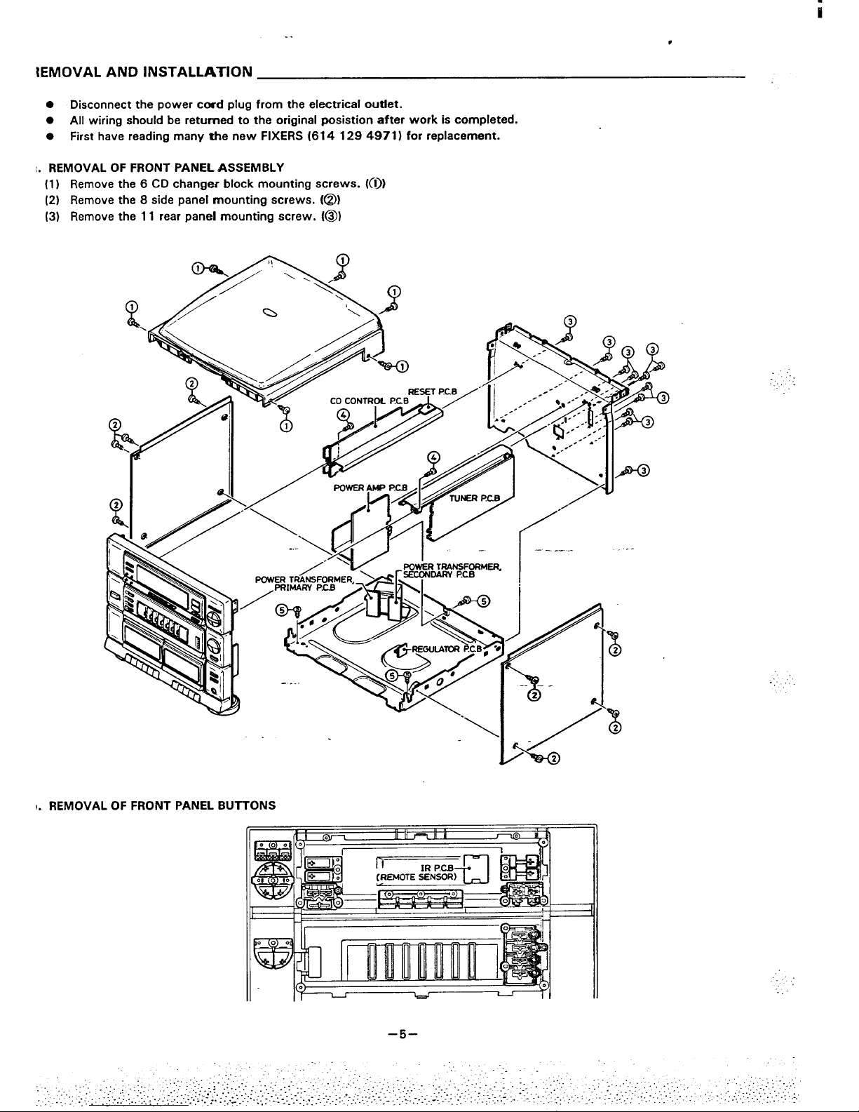
{EMOVAL AND INSTALLATION
. Disconnect the power cord plug from the electrical oudet.
● All wiring should be returned to the original posistion after work is completed.
. First have reading many tie new FIXERS (614 129 4971) for replacement.
I. REMOVAL OF FRONT PANEL ASSEMBLY
(1) Remove the 6 CD changer block mounting screws. ((0)
(2) Remove the 8 side panel mounting screws. (@)
(3) Remove the 11 rear
panel mounting screw. (@))
). REMOVAL OF FRONT PANEL BUTTONS
. . ..
‘.,,
., .,..
.’. ....
....
-5-
Page 7

,..
.
#
REMOVAL
AND INSTALLATION
c.
REMOVAL OF TAPE MECHANISM & P.C. BOARD
(1) Remove the 2 tape
deck P.C.Board mounting screw.
(0)
(2) Remove the 6 tape mechanism mounting
screws. (@)
A
d. WIRING IAYOUT
DISC TABLE SENSOR P.C.B
... .
-...
-A
——
—— .
(a) CD MECHANISM BLOCK
*
.—. — —.
>—’ “-”-”-
, ,!c-
. Arrange the wiring as shown in the figure.
h
.
MARK@
YELLOW m /
rGRAY
..,..,
...
‘“FL-i&ii!sI
\\ \ \\
A
%
-6-
:: TABLE MOTOR
Page 8
ii
..
●
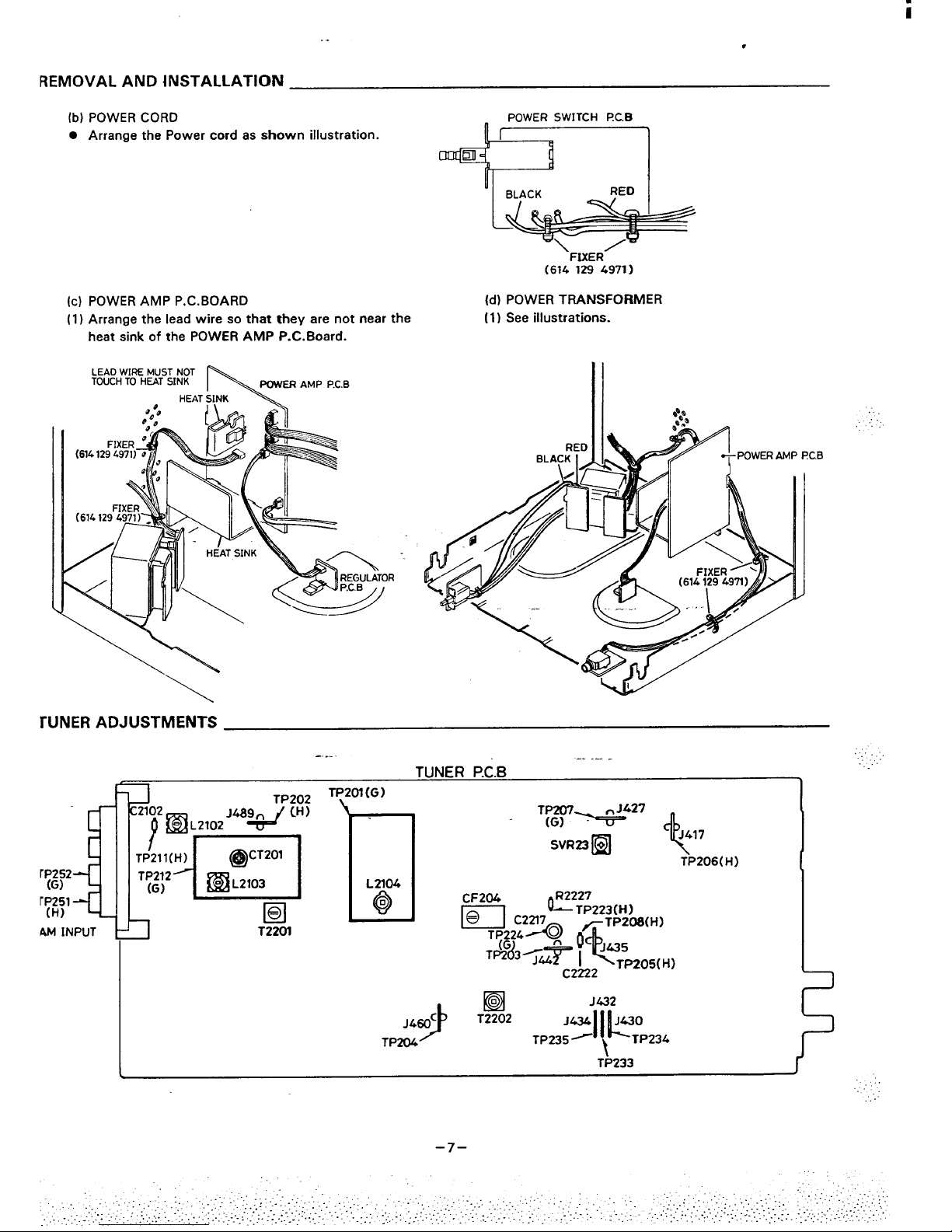
REMOVAL AND INSTALLATION
(b) POWER CORD
.
Arrange the Power cord as shown illustration.
(c) POWER AMP P.C. BOARD
(1)Arrange the lead wire so that they are not near the
heat sink of the POWER AMP P.C. Board.
LEAD WIRE MUST NOT
TOUCH TO HEAT SINK
N
POWER AMP P.C.B
HEAT SINK
rUNER
.
\\
\
POWER SWITCH PC.B
+~gy.
m
BLACK
RED
\ /
\
/
FXXER
(614
1294971)
(d) POWER TRANSFORMER
(1) See illustrations.
ADJUSTMENTS
.
----
-. .-.
TUNER P.C.B
1
J’
I@l
’432
J&Oc
T2202
J434
IL
’430
TP204
TP235 -
\
TP234
TP233
,.
,.. .
.....
..
....
“.
Page 9

I
.-
●
TUNER ADJUSTMENTS
● Use a plastic screwdriver for adjustment. . Speaker impedance
8 ohm
●Standard Output
50
mW
●FM MODE switch STEREO
. TUNING : FM : 87.5-108.0 MHZ ( 50 kHz step ), AM: 531 -1701 kl-lz ( 9kHz 5teP )
“M ANTENNA :
Dummy 750hm U
lalance
VTVM
Oscilloscope or
DC voltmeter
flax.
V-curve)
FM ADJUSTM
T
Adjusting
Iep
Circuit
UT
BAND SELECT SWI1
Connections
i
: FM
SG Frequency
Position of tuning dial
I
Adjustment
input
output
connect sweep
generator to
TP 223 (H),
TP 224(G)
(V-curve)
[S-curve: not adj.)
Connect to Digital
DC voltmeter
TP 202 (H),
TP 201 (G)
Connect to VTVM,
Speaker output
Connect to Digital
DC voltmeter
TP 203
,TP204
( not Ground)
:onnect sweep
]enerator to
[P211 (H),
rP212 (G)
k
T2201
98.1 MHz
-----
~
1
IF
2
Detector
3
Tuning
4 Coverage
10.7 MHz
1.2to.lv)
less than
8.5V)
-+H-+-
87.5 MHz
108.0 MHz
-------
...
90.0 MHz
L2102,
L2103
106.0
MHz
CT201
90.0 MHz
~onnectto
rp211 (H),
TP212 (G)
i
5
Tracking
6
Max.
Ovto.osv
106.0 MHz
Zonnect to
rp211 (H),
98.0 MHz
(66 dB)
98.0 MHz
T2202
1-
7
Ov
Vco
8
(19.00kHz)
rP212 (G)
—-—. .
1
-----
98.0 MHz
SVR23
98.0 MHz ..
(66 d8)
Modulation :
OFF
..
Connect to
TP206 (H),
TP207 (G)
19.00 kHz
f 513Hz
-----b-
. CHECKING THE AM BAND
SG MODULATION :1 kHz, So”/o,
IRE LOOP ANTENNA
,.
....
I
VTVM
Connections
SG Frequency
Position of tuning dial
output
Adjusting
Step
Circuit
Adjustment
I
Oscilloscope or
DC voltmeter
Input
Connect sweep “ Connect sweep
generator to
TP 208 (H),
1
450 kHz
999
kHZ
(CF204)
(CF204 :
adjusted)
generalor to
-1_
1
IF
TP 251 (H),
TP 252 (G)
TP 207 (G)
Connect Digital
1
==4 “1-1”5V)
DC voltmeter to
TP 202 (H),
TP 201 (G)
---.---
3
Coverage
----- I (Iessthan
I
8.5V)
I
T
4
Tracking
5
Connect to VTVM,
603 kHz
603 kHz
Speaker output
1404k Hz
1404 kHz
Connect AM SG
to Test Loop
+
-----
-----
1
Checking the
Connectto Digital ]
I
6
SD
(Auto stop
sensitivity)
Connect AM SG
to Test Loop
voltage
2. O-4.OV
(at 85dB tBdB)
DC voltmeter
TP 205 (H).
999kHz
999 kHz
TP 207 (G)
..---
–8–
Page 10

ii
.-
V
‘APE DECK ADJUSTMENTS
‘REPARATION FOR ADJUSTMENTS
AC; vCXTME T:R
, SCC+E >
1)
2)
3)
4)
5)
6)
7)
8)
9)
I)
pleasuring instruments, tools.
Test tape
MTT-114N (10
kHz)
r;il pill
-.—
TCW-211 (1,500 Hz) (Optional)
MTT-111 (3.000 Hz)
TCC-130 (DOLBY TAPE)
AC-224 (NORMAL)
OEcrrP.C.B
f
AC-5 13 (CrOz)
o
CNO06
o-
“0
L-CH E R-CH
o
Oscilloscope : (At least 10MHZ, dual channel)
TAPE OUT
Digital voltmeter (Input impedance 1MQ or more)
Automatic distortion analyzer or AC voltmeter
(–80dB, input impedance 1MQ or more)
AF-oscillator (400 Hz, 500mV RMS)
Frequency counter (5MHz; or more)
o
Frequency counter, probe.
1
Screwdrivers (non-metallic) for adjustments.
DC digital voltmeter
HEAD REPLACEMENT AND AZIMUTH ADJUSTMENT
A)
1.
2.
3.
4.
B)
1.
2.
3.
4.
c)
1.
2,
3.
4.
5.
6.
Head replacement
After replacement, demagnetize the heads by using a degausser.
Be sure to clean the heads before attempting
to
make any adjustments.
Be sure both channels ( 1 and 2) are the same level
(Using a dual-channel oscilloscope).
All wiring should be returned to the original position after work is completed.
-..
Phase alignment
Prepare a dual-channel oscilloscope.
Set so that the left and right ranges of the oscilloscope are the same.
Play the test tape (MTT-1 14N, etc.: 10 kHz).
Adjust so that the waveforms for the left and
right channels are in alignment, as shown in the illustration.
TAPE “ A “, “ B “Head azimuth adjustment
Load a test tape in Tape Deck * A “
(MTT-114N, etc.: 10 kHz) for azimuth adjustment.
Press the PMY (>) button.
Use a flat-tip (–) screwdriver to turrr the screw
for normal azimuth adjustment so that the left
and right outputs are maximized et the same
phase during playback.
Press the STOP button.
Repeat procedure for tape Deck” B‘.
After completion of the adjustment. use thread-
Iock (TB 1401 B) to secure the azimuth-adjustm-
ent screws.
TAPE “A”
PLAY HEAD
RED
WHITE
FROM CNO09(4P)
BLACK
CONNECTOR
..
....
.-.-- .-
TAPE “B’”
E. HEAD R/P
HEAD
SROWN
WHITE
PINK
YELLOW
RED
ra
f. ~ J
FROM CNO1O(7P)
AT
CONNECTOR
BLUE BLACK
~PLP.. .
TAPE ‘W
AZIMUTH
A
..
:’,
.,. .
...
,.
.’...
. ..
,.-.
..
.;:-..
.:
–9–
Page 11
ii
.-
*
TAPE DECK ADJUSTMENTS
It)
CHECKING THE MECHANISM TORQUES
1. Clean the head, capstan and pinch roller before making any measurement.
Meawing Item
Take-up torque
Back tendon
Tape tendon
Cassette for PLAY:TW-211
1
PIAY:TW-211 1
Drive-power cassette
measurement F. FWD/REW:lM/2231
TW-2412
PLAY
3@60gr”cm
1.5-4 .5gr*cm
60gr or more
F. FWD/REW
55- 120gr “cm
IU) MOTOR REPLACEMENT AND SPEED ADJUSTMENT
A) Motor replacement
/
u
1. See illustration at right.
Q
Q
o
*A
>
,@
B) Motor speed adjustments
1. Make the adjustment near where the test tape
finishes winding.
‘~ T&*p
\\
2. Be sure to make the adjustment of the motor
i
k+
*/
speed only after completion of the high-speed tim-
ing adjustment for tape deck A and tape deck B,
and then making the normal-speed timing adjust-
bfl ‘\
ment
of decks A and B.
‘~ ‘---x 7
...
...
OECK F!C.B
o
CNOOS
o
“o
L-CH E R-CH
o
TAPE OUT
-. —...
❑KOOTED”” -
\“” ~---
HIGH SPEED 21
TEST POINT #n CNO05
f 1
NORMAL SPEED
SHORT
HIGH SPEED
(1)
(2)
(3)
(4)
(5)
(6)
(7)
Insert the test tape (MTT-1 11, etc. 3,000 Hz)
into tape deck A.
Press tape deck A’s PIAY button.
Adjust SVROO1 so that the frequency counter
shows a reading of 3,000Hz.
Press tape deck A’s STOP button.
Insert the test tape into tape deck B.
Press tape deck B’s PLAY button.
Checking the frequency counter shows a reading
of 3,000 Hz (-40, + 70Hz).
Press tape deck B’s STOP button.
(1)
(2)
(3)
(4)
(5)
(6)
(7)
Insert the test tape (TCW–2 11, etc. 1,500 Hz optional). into tape deck A.
Prass tape deck A’s PLAY button.
Set to the high-speed condition.
Short-circuit test points CNO05 pins 1 and 2.
Checking the frequency counter reading is 3,000
Hz.
Press tape deck A’s STOP button.
After the completion of the adjustment, remove
the short-circuit between test points CNO05 pins
1 and 2.
–lo–
Page 12
.-
V
‘APE DECK ADJUSTMENTS
. Make the following adjustments after first cleaning the head assembly and checking the adjustment of
the head azimuth.
f
w
47K 47K
PARTS LOCATION
DECK I?C.B
o
(J
BIAS
SVR504 SVR604
(’-CH); (R-CH)
o
!DQ
REC I PLAY GAIN
SVR603 SVR503
(F?-CH) (L-CH)
1
I
I
Adjustment Item Test tape
DOLBY Meeeurlrrg
Input
output
Adjustment
Adjustment
NR SW. Instrument connection
connection
location
value
TCC-130
(TAPE”A”) SVFM02,
‘a) :?$&@’Jt [DOLBY
OFF
AC-voltmeter
TAPE OUT
SVR602
(CNO06)
(TAPE%”) SVR501,
540mV
TAPE)
SVR601
lb) Recording/
plsybeck
AC-224
OFF
AC-voltmeter VIDEO SVR503,
gain
(NORMAL)
AF-oscillator – 14dB, lkHz
SVR603
O * ldB
adjustment
-.
., .
.- —— ..-
-.. .
k) Recording/
AC-224
AC-voltmeter VIDEO
O * IdBat
playback
(NORMAL)
OFF
SVR504.
AF-oscillator –34dB, 1kHz, 10kHz
lkHz and
frequency
SVR604
10kHz
response
edjuatment
[ ) AMPLIFIER ADJUSTMENTS 5.
A)
1.
2.
B)
1.
2.
3.
4.
Playback output adjustment
TAPE “ A n
- ..
Play the test tape and adjust SVR502 (L-channel)
and SVR602 (R-channel) so that playback output
becomes 540 mV.
TAPE “ B “
Play the test tape and adjust SVR501 (L-channel)
and SVR601 (R-channel) so that playback output
becomes 540 mV.
Recording/playback frequency gain adjustment.
DOLBY NR switch : OFF
Input signal :
– 14dB, 1
kHz.
Tape to be used :
NORMAL (AC-224, etc.)
Introduce input signals to the VIDEO terminals,
and, with the unit in the REC. PAUSE mode, adjust input level for 3dB out,
Record the input signal.
Press the REWIND button and rewind the tape to
the beginning of the recording just made.
Press the PLAY button.
6.
c)
1.
a)
b)
c)
d)
e)
f)
-11–
Adjust SVR503 (L-channel) and SVR603 (R- chan-
-..’...
.,
net) so that the recording and playback output level differences become * 1dB.
,’.:...-
‘........
Repeat steps (1) to
Recording/playback
ment. “
DOLBY NR switch
NORMAL TAPE
Tape to be used :
Input signal :
(5).
frequency response adjust-
: OFF
NOFWIAL (AC-224)
-34dB, 1kHz, 10 kHz
.....
introduce input signals to the VIDEO terminals.
With the unit in the REC. mode.
Record these input signals {1kHz_
10kHz
— 1kt-fz
—lokJ-tz).
Press the REWIND button and rewind the tape to
the beginning of the recorchg just made.
Press the PLAY button.
Adjust SVR504 (L- cttarwwl) and SVR604 (Rchannel) so that the 10 ki-tz and 1 kHz output Iev- . “
.
el differences become * 1dB.
Repeat steps (a) to (e).
Page 13
ILLUSTRATION OF CD CHANGER MOVEMENT
. This CD changer can accommodate and play up to 5 discs.
a. OPERATION
1.
“ POWER “ ON.
2.
“ FUNCTION “ CD.
3.
“ DISC SELECT “ 1.
4. The sub chassis (27) move$ down.
5. The disc table (82) turns, and the disc 1 table is
brought directly above the mechanism where it
stops.
6, The sub chassis moves up, the disc is chucked, the
turntable (11 -1 ) rotates, the disc’s TOC (table of contents) is read, and the turntable then stops.
If a disc has not been intalled, ” no disc “ appears on
the display.
7. When” DISC SKIP” is pressed, steps 4 to 6 are performed, and operation advances to the next disc num-
ber.
----,.
,.’
-.
b. NAME AND FUNCTIONS OF MAJOR PARTS
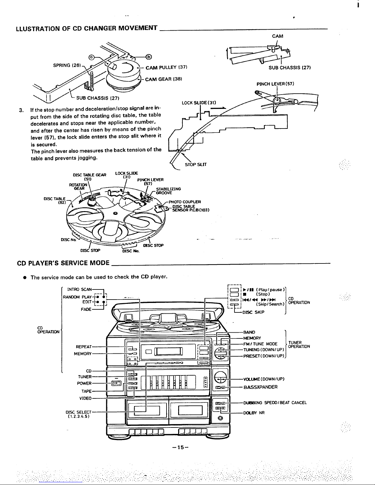
1.
Disc table (82)
Disc number detection slits 1 to-5 and a stop ~e~ec-
tion slit are cut into the outside circumference of the
disc table.
These slits are used by th_ephoto coupler to detact
the disc number, deceleration timing and stop poai-
-..
tion,
Also provided on the circumference of the table
area
stabilizing groove and rotation gear.
DISC
..’
DISC Tft3JE GEAR
LCc~3S}loE
I
PINCH LEVER
Jxsc’ STOP
K% No.
-12-
i
Page 14
i
.+
●
.LUSTRATION OF CD CHANGER MOVEMEMT
2.
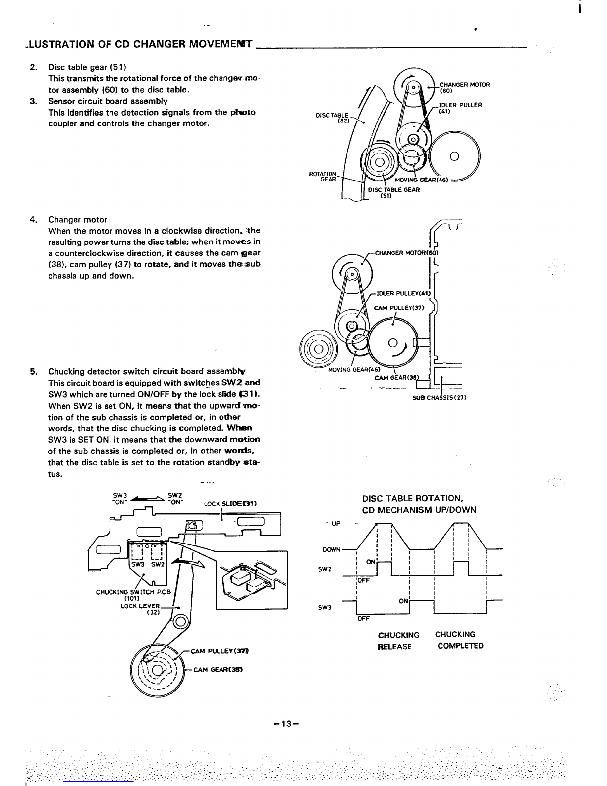
Disc table gear (51 )
This transmits the rotational force of the changew motor assembly (60) to the disc table.
3. Sensor circuit board assembly
This identifies the detection signals from the pfmto
coupler and controls the changer motor.
4. Changer motor
When the motor moves in a clockwise direction. the
resulting power turns the disc table; when it mowes in
a counterclockwise direction, it causes the cam gear
(38), cam pulley (37) to rotate, and it moves the sub
chassis up and down.
5. Chucking detector switch circuit board assemb%
This circuit board is equipped with switches SW2 and
SW3 which are turned ON/OFF by the lock slide 631).
When SW2 is set ON, it means that the upward wno-
tion of the sub chassis is completed or, in other
words, that the disc chucking is completed. Wham
SW3 is SET ON,
it means that the downward motion
of the sub chassis is completed or, in other womls,
that the disc table is set to the rotation standby status.
- .. .
If?-’‘
LOCK LEVER [
(32)—
0
<-~--.,
CAM
PULLEY (3X$
~,,i,$>
CAM 00S(3S3
\ ~s_/
‘ ,/
‘.-__~
<,
Lb
@
;~#WER MOTOR
. ...
IDLER PULLER
DISC TABLE
(41)
(82)s
/- (”-.
~)
o
“m “-
@ ‘c
o
\
ROTATION
-—. .
GEAR
MOVING GEAJ?(46)
—.—
P
r
SUB CHA&1S(27)
.. .-.
DISC TABLE ROTATION,
CD MECHANISM UP/DOWN
-UP -
:OFF
i{
1
I
1
I
U---H
! 1 , ,
I
I i I
t
SW3
OFF
CHUCKING
CHUCKING
RELEASE
COMPLETED
.
Page 15
,.,.,...
.-
#
ILLUSTRATION OF CD CHANGER MOVEMEIW
6.
Limit switch (9)
This switch is provided on the CD mechanism (1 U) to
stop the pickup at its precise home position.
The sled motor (12) moves the pickup via the pcsanmr
gear(2), mid gear (3) and rack gear (1-2) which ~*cured to the pickup. Moving toward the center -m
the outer circumference, the pickup sets the Iimilt
switch ON at the end of the rack gear, opens the ‘CD
main circuit board (91 ) circuit, moves forward f=r
about 10ms and then reverses.
The rack gear which movas in reverse sets the &rmit
switch, OFF, moves forward for about 10ms and
then stops.
c. ILLUSTRATION OF CD PLAYER MOVEMENT
1. The sub chassis (27), which is secured by the CEl
mechanism, is pulled upward at all times by tensaicm
.,
spring” L” (26), and tension spring U R “ (28), and it
is kept in place by the cam puny (37), lock slid, smc.
2. The rotational force of the changer motor is ap@ed
to the moving gear and idler pullyed secured to the
moving lever.
The moving gear performs two differant operations
depending on the direction in which tha canger rrtswor
is rotating.
When the motor is rotating clockwise, the gear
causes the disc table to rotate through the disc table
gear; when it is rotating counterclockwise, it roustes
the cam gear and cam pulley, and jt moves the =b
chassis up and down. At the same time, it activates
the lock Iaver, which is linked to the cam on the bottom of the cam gear, and then the lock slide in mm.
. .
L
J
“ON-
““OFF““
FORWARO@-----
SLED MOTOR
ROTATION
‘RET”N)==l k
REVERSE @
. . .
I
I I
Revolution
,., ---
...__ ___
---- -
. .... .. ..
LOC% SLIDE(31)
— ‘1
M
—
-sPR1NG(28)
t
u
,
T.
CAM GE& (38)J
CAM PULLEY(37)
1
- ~~~
SUE tHASSIS (27)
,.
...
–14–
ii
Page 16
..
*
LLUSTRATION OF CD CHANGER MOVEMENT
CAM
~>>L
1~~
SPRING (26) l~/L~Y cm PULLEY (37)
SUB CHASSIS (27)
3.
&f~~&&-.A.GEAR,~*,
SUB CHASSIS (27)
If the stop number and deceleration/stop signal are in-
put from the side of the rotating disc table, the table
decelerates and stops near the applicable number,
and after the center has risen by means of the pinch
lever (57), the lock slide enters the stop slit where it
is secured.
The pinch lever also measures the back tension of the
table and prevents jogging.
DISC
DISC TASLE GEAR
LOC~3S#E
(51)
I
PINCH LEVER
PINCH LEVER (57)
LOCK SLIDE (31)
TA
103)
DISC STCP
DISC No.
CD PLAYER’S SERVICE MODE
. The service mode can be used to check the CD player.
CD
OPERATION
.—
...
.. ... ...
~----
INTRO SCAN
7
~0 1>/88 (Play/pause)
..— ~
RANDOM PLAY+ I -.
7
EDIT++
I
L
I
I
FADE
“%- ‘Ezks’rch)
1
_l:
—.
&hATION
-15-
TUNER
OPERATION
.
.
“, ..
.......
......
:..’.
.:, ,
Page 17
.-
●
CD PLAYER’S SERVICE MODE
a. THE DISPLAY WHEN THE KEY SWITCH HAS BEEN F%EESSED
(1)
(2)
(3)
(4)
(5)
(6)
Turn the POWER switch to “ ON. “
Switch the unit to the service mode by pressing “%kre
tuner’s” MEMORY” key within one second afmsw
pressing the CD player’s “ MEMORY” key and ftkaa
tuner’s” BAND “ key simultaneously.
When the tuner’s” BAND “ key is pressed, the Uf2D
reads” REC “to indicate that the key input has be?em
registered.
When the tuner’s” MEMORY” key is pressed, @we
LCD, in addition to “ REC “ described in (3) ab~,
also reads” TIMER”.
Thus, as shown in the table below, the characters
and symbols displayed on the LCD increase as lb
corresponding keys are pressed.
To cancel the service mode, press the “ FM/TUP$fE
MODE “ key .
I
KEY BUTTION
I
LCD INDICATED
1
KEY BUTTON
I
LCD INDICATED
(TUNFRI lcn~
I
BAND
REC
MEMORY PROG.
MEMORY
TIMER
REPEAT
FNVTUNEMODE
REPEAT
[To cancel the
PLAYIPAUSE
D
service mode)
TUNING ‘ UP 8 SLEEP
9TllP
TUNING “ DOWN “ CONT
PRESET“ UP w SIDE
A
++
PRESa wDOWN “ SIDE B
(CD) DISC SK
RANDOM PLAY ‘“-
pANnC)M Enlr
INTRO SCAN
INTRO I
I
C)NF
----
1
----
➤>
DISC
I
TRACK
I
I
(IP
I
ALL .,,
I
I rnlr I
.“ . .. -----
I
--, .
I
--, .
I
I 1
I
.——
(DISC”SELECT)
(PROG-tiM)
I
(FUNCTION)
(PROGRAM)
--
TUNER ii
3
3 TAPE
15
4
4
VIDEO
➤
5 5
-._.
-. .-.
b. CHECKING THE MOUNTING OF THE LCD’S PRINTED CIRCUIT BOARD
(1) Turn the POWER switch to “ ON ‘.
(2) Switch the unit to the service mode by pressing the
CD pjayer’s” REPEAT” key within one second after
.-
pressing the CD player’s “ MEMORY “ key and the
tuner’s “ BAND “ key simultaneously.
COMPUTEITflEC,
WIOECLOCI(INTROtiDOM OFFSIOEA
(3) Confirm that one segment of the LCD comes on
SLEEP‘–/-///~/, /-/ /~/ ~~lz 5//-/ /-/./-/ III ~~ZS~~EI
WAKE UP
each time the CD player’s “ REPEAT “ key is
LEVEL/l/@Jk/:/ Is/ LWAM-I1;1Iil:lil /2/ MI PM
TIMER
RECDISC ST TRACK AUTO MONO FAOE TIME EOIT
pressed.
D
(4) To cancel the service mode, press the” FM/TUNE
EjEEi123456789101112131415~i%EiLCONT
MODE” key.
-16-
Page 18

.+
v
D PLAYER’S SERVICE MODE
TEST D[X
CHECKING
(1)
(2)
(3)
(4)
(5)
(6)
(7)
(8)
THE CD PLAYER’S OPERATIONS WITH THE
LCD’S
Set the CD player to disc table “ 1 “.
Press disc select key * 1 a.
Preparations for setting the unit to the” PLAY “ status are now complete.
To check the operation mode, switch to the service
mode.
Turn the POWER switch to “ ON “.
Switch the unit to the service mode by pressing the
CD player’s “ STOP “ key within one second after
pressing the CD player’s “ MEMORY “ key and the
tuner’s “
BAND “ key simultaneously.
The numbers (O through 5) that appear in the LCD’s
“ DISC NO, “ indicate whether the CD player is oper-
ating correctly or not,
[f a malfunction exists, refer to the table below to
de-
termine the nature of the malfunction.
NUMBER DISPLAY
DISC NO.
1
l-- \
.—— .
—
—
awurw
1
WUH(I(XX
IN HIO llANIXIM WI” SIOE A
SEEP
~M~ ,,,,-/-/ /:/ /:/ /:/ VW’ ~ _/ /:/ /:/”/:/ /:/ fllsyfio
I L~v~L
I_I/_/ [_/ /_/ ,,WAM/ /_/ /’_/:/’_/ /_/ Mll, IIM I
IIMIW IICC IIIS(; S1 [11A(:I( A(I ((l MONfJ F~ Tlw11)1[
L
D
-J
mlz3456? 8g1011121a 1415 F%T~[LCONT
—
— —
I
LCD
DISC NO.
I
CD ERROR MESSAGE
1
I o I No malfunction I
1 The pickup’s laser was not focused properly during a focus search.
2 The sub-code could not be read when the disc began spinning.
3 The TOC (table of contents) could not be read.
t
4 I The focus was lost when the servo was on (e.g. ~during playing). ... .
5 I The sub-code could not be read when the servo was on. (e.g., during playing).
“ TRACK NO. “in
the LCD indicated how far the CD
player’s operations have progressed.
LCD
TRACK NO.
CD OPERATION
-. ....
..
00 FOCUS SEARCH START
,
01 i FOCUS SEARCH START I
02 The ufit iswaiting for the pickup’s laser to focus during a focus search.
03
Focusing of the pickup’s laser during a focus-search%as been completed.
04 The kick when the spindle motor begins rotating.
05 CLT (Constant liner velocity)
and Tracking “ ON-”
06 CLT and Tracking “ ON “
o- FOCUS SEARCH END
30 I Brakina of the sDindle motor is beraun. I
..-.
,.’
4
40
➤> (FWD, SKlp/SEARCH)
41
+< (REVERSE, SKip/SEARCH)
50 PLAY
51
PLAY
52
PLAY (music skip)
... ,’.
‘.. .
-17-
Page 19

.-
●
CD PLAYER’S SERVICE MODE
LCD
TRACK NO.
CD OPERATION
60 Reading of the TOC (table of contents) is begun.
61 Reading of the TOC is in progress.
62 Reading of the TOC is in progress.
6-
Reading of the TOC is in completed.
85 Pausing is begun.
86
Pause
I
I
90 I A CD track is accessed.
9’9
I
I A CD track is accessed.
9A A CD track is accessed. (final stages)
9–
A CD track is accessed. (final stages)
AO CD mechanism moves down
A2 The turn table besrins s~inning.
A7 The turn table sp-~s at low W-eed.
A8 CD mechanism moves up
A9 CD mechanism chucking
,
t
A–
I Chucking of the CD mechanism is completed.
1
(9) To cancel the service mode, press the” FM/TUNE
(lo)
MODE “ key.
..-
Turn the POWER switch to “ OFF”
., ..-
..——__
d. HOW TO ADJUST THE CD PLAYER’S TRACKING BALANCE IN T {E SERVICE MODE
.
Refer to pages 21 and 22 for instructions on adjusting
without using the service mode.
. Adjustment is easier in the service mode because it is not
necessary to repeatedly press the FORWARD SEARCH
button.
. ...
-. .-.
(1)
(2)
(3)
(4)
(5)
(6)
(7)
.-
..
‘.’.
t
I
Connect an oscilloscope to TP103 (TE).
Switch the unit to the service mode by pressing the
CD player’s” PLAY/PAUSE k key within-one second
after pressing the CD player’s” MEMORY” key and
the tuner’s” BAND” key simultaneously.
Program numbers” 1 ‘and m 15 “on the LCD come
on, and the unit enters the service mode for adjust-
ing the tracking blance.
Play the test disc.
Using an oscilloscope to measure signal TP103
(T.E.), adjust SVR 11 so that a vertically symmetrical
wave-form for the OV level is obtained.
if the wave-form is
not vertically symmetrical 4ilce
the one shown in the illustration, press the CD
player’s” MEMORY “ key to adjust SVR11.
Press the stop button.
-18–
CD MAIN F?C.B
... .. - .
E
TPIOl(RF)
TPI02(FE)
TP103(TE)
TPIW(GND)
a
SVR1l
TP103 O
(+)
I SCOPE I
TP104 O
(-)
I
TP103
Ov
(TE)
Page 20

ii
.-
*
1 PLAYER ADJUSTMEIUTS
(a)
●
●
●
(b)
Replacement of the pickup
solder for
Note that the mechanism of the CD player is very
short-circuiting
delicate.
the patterns
When handling the pick-sap. take care not to exert excessive force, and particular care should be taken
t
not to touch the lens or tEwedrive circuit’s printed* ir-
U
w
cuit board pattern.
In order to prevent da-e by stati
ing shipment, the indic-d pattern
P.C. Board are short-circdted by so
After the pick-up replacement, rem
that is short-circuiting the patterns
Replacement and Iubric*n of the CD mechanism
I
(BE SURE, AT THIS TIM=, NOT TO
POWER GEAR
I
,...L<=
MIDOLE GEAR
EM-SOL
+1
w
SLED MOTOR “ -
-. .
Iote:
M-50 .“””.”.”.””””.”
MOLYKOT& EM-50L
G-7
............... SANGREASE, SG-7
149p
............... FLOIL OIL, 949P
TOUCH ANY OTHER PART. )
( SHORT)
u
4J!3
=%@E
(OPEN)
-19-
,. .-..
-...,..
...
.’. .
.,:
Page 21

i
.. :
CD PLAYER ADJUSTMENTS
(c)
Replacement and lubrication of the CD changer
CAM PULLEY
After Insert gear [ever and special washer, apply
MC-grease EMSOL to 113 length portion of shaft
WASHER
w
-.
EMSOL
—~
MOVINGLEVER
VIEW-A
I
I
After insert gear lever to shaft,
Lever in set under the ribs
P
&
J -“”
—.
-..
id ? ILLAI -–_
J&-=-k
-----
GEAR, DISC TABLE
EM50L—
. .
CHASSIS, SHAFT
~LY&kft7
q>
@
0°0
--& .0
-.
1
t);
8.95 tO.1 mm
DISC TABLE
MOTOR.
–20–
Page 22

ii
..
#
D
PLAYER ADJUSTMENTS
PREPARATION FOR ADJUSTMENTS
1)
Measuring instruments, tools and filter
) Test disc :
F30L-50146 (Poly Gram) etc.
!)
Oscilloscope : SS5711 (1 O MHz or dual phenomenon) or,
Memory scope : DSS6521 (Storagescope)
I) AC voltmeter (–80dBt input impedance 1MQ or
more)
H AF-oscillator (400Hz, 500mV RMS)
;)
Screwdrivers (non-metalic) for adjustments.
j)
Band pass filter
. PARTS LOCATION
-----
.....
COMAIN PC.B
IF
TP101(RF)
TP102(FE)
TP103(1E)
TP1043ND)
-$&
IOTE: 1. All measurements are referred toTP104 (GND).
2. Adjust SVR11 is initial setting position, as shown in the illustration.
.
.-. .— -
:. ADJUSTMENTS
Adjustment
Test
Measuring
Input
output -
- Adjustment
Adjustment
Item
disc instrument
connection
connection
location
value
(a) Tracking
TP103 (TE)
Waveform
balance
Oscilloscope
...............
TP104 (GND)
SVR11
symmetrical
adjustment
F30L-
referred to OV.
(b) Checking the
50146
Memory scope
IC101 @ (H),
TP102 (FE) .... ......... ..
500m Vp-p * 3dB
focus gain
Oscilloscope
TP104 (GND)
TP104 (GND)
(c) Checing the
Oscillator
Band pass
IC101 @ (H),
TP102 (TE)
....... ........
500m Vp-p * 3dB
tracking gain
filter
TP104 (GND)
TP104 (GND)
(d) Checking the
TP101 (RF)
.... ...........
Oscilloscope
....... ........ “ Eye n pattern.
eye pattern
TP104 (GND)
... .
-21–
Page 23

i
.-
8
CD PLAYER ADJUSTMENTS
(a)
(1)
(2)
(3)
(4)
(b)
(1)
(2)
(3)
,.
(4)
(c)
(1)
(2)
(3)
(4)
(d)
—
Tracking balance adjustment
Connect an oscilloscope to TP103 (TE).
Play the test disc.
Push the FORWARD SEARCH button.
Keep the button pushed and adjust SVR 11 (T.
Balance) until the track-jump TE-waves on Tpl 03 are
symmetrical referred to OV.
Checking the Focus gain
Connect an oscilloscope via the band-pass filter to
TP102 (FE).
Play the test disc.
Connect an AF-oscillator via a 120k ohm resistor to
pin 24 of IC1OI.
Frequency = 400Hz, amplitude = 500
mV RMS.
Check the average 400 Hz FE-signal amplitude on
TP1 02, measured through the band-pass filter, is
500m Vp-p * 3dB.
Checking the Tracking gain
Connect an oscilloscope via the band-pass filter to
TP103 (TE).
Play the test disc.
Connect an AF-oscillator via a 47K ohm resistor to
pin 140flC101.
Frequency = 400Hz, amplitude = 500 mV
RMS.
Check the average 400 Hz TE-signal amplitude on
TP1 03, measured through the band-pass filter, is
500m Vp-p &
3dB.
-.....
Checking the eye pattern
The adjustments (a)-(c) complete the adjustments of
the CD player.
Next, check the eye pattern wavetorm.
TP103
(+)
o
SCOPE
TP104 O
(-f
TP103
(TE)
T’=%EI
Iclol @
B.P. F.
(+)
~,
TP102 0
IN
TP104 o
(-)
TP=$LEI
Iclol @
B.P. F.
..-(+)
(+)
7
TP103-0
IN
OUT SCOPE
TP104 0—<
(-)
T
Measuring
Test
Output connection
instrument
disc
“ Eye “ pattern
point
● Check to be sure that the” eye U pat-
Oscilloscope
F30L-
TP101 ((RF)
tern is at the center of the waveform
50146 TP104 (GND)
and that the diamond shapeis clearly defined.
,,.
,...
...
....
–22-
TP101
(+)
0
1
Page 24

i
.-
#
XPLODED VIEW (CABINET & CHASSIS]
r.
,---
......-
.. ..
., ...
“.....
......
...::.,
Page 25

Page 26

–9z-
..
.
-Lz-
3M11OO’NO1M8
301S lH91h’’lNOLi4”3-13X3W3
mmu,Noms
AMOW?N4cWa”Nolln8
3131S1331’lNOW ‘3-13XNM8
k’:,Md”NOUnE
011 3113SSU3”Assw W39
lNOW’13NVd’.ASSV
M01V310NINOIIISOd 3K?1OA’I!OONIM
91A
$M
9LA
flA
ZIA
11A
OIA
60A
80A
LOA
90A
SOA
90A
ZOA
10A
0N”43U
9NZXU
91LSsL 30010
K Lss1 30010
lobu9 3aoIo
9flSSl 30010
609$ Z1O 10!I
90?? Zlo ,!0?
?066 LOO LOV
600S ZLO LO?
9077 ZLO 10?
?066 LOO LO?
0010 S01 LO?
9S59 LOO 7t9
KSZ L1O 919
L49Z LIO ?t9
MO
80
10ZZI3
89
Zo
+/Oizo
10LZO
10Z1I
Z9ZN3
1?zti3
LOZN3
Sozil
*ozj3
ZOZ33
Lozsl
8S?’Z2
90ZZ3
u0133NN03
L’7ZN3/\SZN1’d0l’S-80133NNOl’ASSV
“8.3”dWt6’ll<d?’13X20S
“E.l”d13NlU’dOL’13X10S
Z091 ?!’Z9L9 KZN3
m? Szo 719
ZSZN3
Lbb? SS0 719
1SZN3
8660 l?Z919 3
Z*
1?
09
6S
8s
LS
9s
SC
K
Es
Zs
1s
0s
63
ez
LZ
9Z
<z
PZ
Sz
Zz
LZ
S1
xl
Z1
11
01
6
W
a’
L
4
9
f
z
L
IN-338
13NIW3
80
“91U Uolloa
L3N18W3’HU8XSN18 9dl-SMIS
..
.,’: ...
...}i.:,..
—
“91U LIUSJ311OE
13NIW3”LiU8XS N18 9dl-S US
“E”3”d L43W04SNWM
SLSSl 3ooIa
(Soizo’?Olzm LOVU930010
(10Lzo-toIzo)
(3-z8)u3flo-i’“91U 031’U3A03
(o-z8)031’u-lNnou
9S99 6SZ 9L9
I
o
9096 ??Z 9L9 3
0?68 OIIZ919
8
I
(3-Z8)031”H3113A”133HS
(8-Z8)031”311Hfl’133HS
(V-Z8) Ulml’ 031
h’3MOd”IW9X? NIg 9dl-S K3S
XtISlV3H 31 “dhv
83fiOd’LJ48X9”Z91+Zb’E 9dl-SK3S
.8.3.d
‘d!.!V83MOd’IW8XS NIS(9dl-S }3S
“8’3’d &!3Nnl’liU8XSNIE 5dl-S N3S
“a”3”d
70U1N03 03’UL18XfN18 9dl-S XX
w-a- L~zms 10 8013wawn
3dlL’U3LiUILN
(ZSZN3)”8”2”dlN083’d?’9nld
(LSZN3)“a”g-d lN08J’dOl’9nld
WNN31NU dOOl H’d
‘UNN31NU-1X3 Uj‘d?‘1VNIH831
u3171j UUW833
ZHX3S?’83171j
ZHUL”OL’U3111j
ZHUl”OL’U3111j
(MS 6 nL 13313-dN
w
KSVawQa.3”duivd~
lN084’83d’ASSW
M311dI#3S30
dIxs/4j’NoLlna
03’dOIS/3SnVd.AUld’NOlln8
13313s 3srofNouna
989L 6S2 IIL9
L9L9 0S0 ?L9
??96 80Z 7L9
66[0 Ifz +/[9
6610 LSZ 919
S091 901 SO?
000s 080 so?
8ZLL 7CZ 919
NW3SOUNI
/Ati7d~ONWUfiOU~/l103”NOlln8
03’A80U3WlW?d38”NOlln8
no
LS?ZX
20ZZ1
Iozzl
Iznns
no
I06Z0
80
Z08Z0
80
t08ZfJ
80
ZOLZO
no
IOLZ8
-no
\99zo
b’o
lS?ZO
80
80
lSSZO
no
MO
Zoszo
no
Iolzo
fozzo
no
Zozzo
10ZZO
S01Z8
!JOlzcl
Mo
SOtzo
Zotzo
no
10LZ!3
ts?zl
OSLZ1
So[zl
?Olzl
SOIZ1
ZOLZ1
SOZ31
ZOZ31
!OZ31
20
80
LS?ZO
80
MO
@
“ON”j3
6899 OkZ 719
S979 09Z 9L9
96?9 O?z PL9
‘91U”8”3”d
13X3WWdNUO
~X9”Z NIfd9dl-S KIS
“a”~-d 13S3U’h!48X$NILISdl-s LLOS
‘9LU mmoa
‘13NVd Wd3U‘!-MOLXS NIE 9dl-S K3S
“91U 13130s
ZHUZ”L’WWNOS3M
ZHNZ”L’M01WNOS38
98?0 !’$2!L9
8[L1 072 9\9
!11? 0S0 7L9
66ZL 6CZ 919
L061 ?OZ ?19
70ZL OZO SO?
Zooz Zto so?
Sozz 910 so?
90ZZ 9LO SO?
?OZL OZO S0?.
Zooz ZLO so?
So:z 9!0 so!
9ozz9to so?
?OZL OZO SO?
Zooz ZLO so?
POzl Ozo so?
0301A
/3dW1/33Nnl/02”NOIllYnj’NOllf18
03010f3d?l/83NflL/03
‘U01V310N1NOI13Nnj’tW30NIN
“.4iU/M3Nnl/03‘13NWd‘ASSW
.U. 3dtJ1’3113SS53’OIl”ASSU
..8.3dV1’3113SSY1’011’ASSU
011’3113SSL?3”281M’9NIUdS
.% 3dVL.NOIlY80330#ASSU
.S. 3dWl”NOILbLd0330’ASSU
0N03 N3?2d3W’U3XIj
“91!4UO11O8’13N18Y3’10034ASSV
U01J084L3NI’dU3
lH913’U-13X3bU8
li31,u-13)3u8a
lH91!d’301S’13NWd
WIS,(WIVNNI 30b,A’Wd38”13NVd
3WV9NIS NI 30%’’MW38’l3NUd
1~31’301S’13NWd
“91U318VL 3SIO”&39Nti+303’133HS
“91U 39NIH”h”JSlX8”NOIHSn3
x3M13 lsno’39mf
ZHNL”OL’”1”4”1
..1.,:1
i?OOlf dOOO\ OHdAIOd
1UNINL131
SO?9 O?z 919
SZz!.z?z ?L9
8ZOL 07Z 919
LLOL 0?Z9L9
LSOO e~z9~9
60Z? Z?Z I/i9
SSOL O?Z 919
1061 6Z1 9[9
C40L 9LZ 719
18Z!I6SZ 919
ZOLZ 07Z ?19
61LZ 09Z 719
01?9 6SZ 9L9
LSL? !I?Z9L9
[890 9?Z 719
SOW6SZ P19
LL9V Zcz YL?
0s80 SZL 9L9
60SZ Ztl ?L9
9LZ9 O?Z 9L9
“ON
lWd
SISSVH3
!+0 XO!’M01SIS3U03X14-IU3S
>-US763SZ81
M9-SL813SZ81
8-8L8Z3SZ Ml
W-8U3Z3SZ U1
W5?63SZ Ml
u9-s18i3szal
301S NU311Ud”31Vld0131HS
(03sllZ)301S S18Wd 0131HS
83Nnl’83d‘ASSW
NOILdIti3S30
4
6ZOt .111?19
6KS 911 7\9
06S0 S!IZ7i9
19
“ON lUUd
“ON”q3t
m
awa”rd w
‘73NVd WJ3U’WOLXS N18 9dL-S N3S
.91u 13x3w8a
‘13NVd w3u.UMOLXE NIE 9dl-S 83S
.91U
13NVd301S’W3XS
N189dl-S 82S
.a.3.d
NIVU 03’WOIXS N18 9dl-S M3S
.91U
W9HW303”liU8Xi
N189dl-S 83S
ZOO!i3
LOO::]
6L
OL
LL
9L
SL
?L
~~
ZL
IL
ON”43U
lIM1331
a-8Laz3sz
w
v-818mz U
H311MSMSINUH33U
3dU1.d9”S-N0133NN02.ASSW
I
Z77981Z 919
H311MS
WS?63SZ W
LL9-<18L3SZU
WW63SZ Ml
WI-SL8L3SZMl
A-(1)SL813SZ W
(ZSK8. LS?ZO)#9-(l)S1812SZ31
SA9L1W1Oal
dYd\N8 81
(ZSSZO’ISSZO)LOZZNUU
WLLV1O W
dWtN8 W
LOZZNU 81
Y-W63SZ 81
KML813SZ ML
Li3-SLOiWSZ81
WS963SZ 81
ti9-S18L3SZ81
O-U1O8S3SZW
A-fZ6L3SZW
A-SZ6L3SZML
11+.61XZ N1
lU-S6[XSZ81
A-fZ6L3SZXl
11-S6t>SZ81
lH-S6C4SZal
,.
NOIldI~3S30 I ‘OH lWd
13313S 3d’dL’d:’S-MO133NN03’ASSV
83ddOlS 13130S S3NOHd”82d
AW4U8d.U3iWOKNVk’l U3MOd’83d
106~4u7.onosz 3snj
LL0133NN03
ZIlN3/SOLN3dd’d‘S-YOL33NN03.ASSV
tio133NNo3
6S?9 81Z’9L9
LS?OS?Z 9i9~
96fe S?z ?L9V
S096 910 SZ7V
ZoozZioso?
S06L 711 S09
7081 ?tlso?
!I060000 SO?
70?Z 8L0 S09
0080 L90 S09
?060 000 SO?
!JObz8L0 so?
0080 L90 S07
?021 Ozo so?
ZOOZ Z1O SO?
XI+ OW31’U3XIJ
.91U 13NVd
OSSL I/?Z719
I
..
SK82LZ 919
ZS99 lLZ 919
9$$0 80Z ?19
806$ 1S0 ?L9
66
0699 tZZ 17L9 z<
KL9 OZZ 919 1s
0fZ691Z !I:9 05
L9Z69tZ P19
6P
%Z69LZ 719 e?
J
6F.Z6?61 ?19
L9
LL169tZ 919 ??
C90691Z ?L9 s?
?Z!6 91Z 7L9
W
81Z08ZZ !L9
Pl
.ON lYVd .ON.j38
31aul 3s104
...NOIIVIOWti3SVl
3181SIhNI..
.NOIlnV3.A13iWS.13$371
.91U
13NVd Llv3ki’1SSW13.A13fdS’138V7
.XU
OV31 USINbH33H’L+10?X0l’NOIHSn2
U3LLtiOjSNVHlN3iW3d’9111
.9Lu 3wnlon
33NVlW8/Li3ZIlVf10331HdUU9’MOONIM
33NU7VS
8 83ZIlVnD321HdV&!J’3011S’130N>
L331’HSINbN33U3dV1’3-13XW#3
L!3ddn’USINVH23U3dW1.3-13X3WM8
U011084USINUH33M3dtil.3-13X3VU8
80NXUSINVH33U 3dV1’13X3V8tl
L9SL 9PZ 9L9
lsno’mY33’Assw
NOIldIM2S30
I
90LN’3/?O[N3‘d~i‘S-L10123NN03‘.ASSV
U0133NN02
11LN3/fOON3’d9’S-L!0133NN03.ASSV
1061.N3UUO3SNVUL L!3fIOd
INIS 1V3H
WL L?’Z!fL9
9SS8 S?Z 9i9%’
0698 LIZ ?19
ZL6Z SZO ?L9~
100L LOO S07
90ZL Ozo so!
3U’0U03 83MOd
No30u3u’AY31Lva”oIl
I
ZCV6SCZ L49
N02+3R3U’ASSU
L<L6 S%z *19
Zooz Z[o so?
Z06L 810 S07
706S ZtO SO?
706SZI0 S09
LO?9 9LL SO?
90s’6PLL so?
906S ZLO SO?
LOW ?lL S0?
90S8 ?LlSO?
9SZ9 8Z0 ?19
Z9LL L7Z 919
8s0? ‘dZo?19
Z8ZL 6SZ ?L9
SL’606ZZ ?!9
9980 6ZZ 719
O09L 990607
00S6 9L0 60?
801S S61 60?
608S ZLO LO?
90?? Zlo ,!0?
?066 LOO LO?
608S ZtO LO?
90?? Zlo 10?
?066 LOO LO?
NOIldIN3S30
I ON lMUd
(011 A8311v8
HIItNlLILINO>31OIQ8’NO2OU3N.,ASSV
l“”
L9Q6 S9Z 9L9
Llv31W’VNN3LNV
1L99 Z’ZZM9
1NOU3 !-iUO\X9Z N18 9dl:~”i~
,.
.a3”dx330wuexs NIa 9dL-SN3S
USINVH33U
3dV1’kU8XfNIfL9dl-S M3S
.!IIUNSINVN33U
3dVl 13X3W3’L+W9XZNUd 9dL-S h’3S
.91W 80NXUSINbH33W
NV”bNN31NVdool
13310LldUSINVH33HO3’33I1ON
lVnNbW NOI13nNlSNI
“13S’13:HS80123108d
13S’L13N133A10d 83NNI
K13110a’owd
9081 lZO 119 O:A
S0?9 LZO lL?
6~A
S079 lZO LL?
8ZA
S06Z 8Z0 Ll! LZ.4
908L lZO lL?
9ZA
SilfsLZO 1[?
SZA
Z08Z ZZO tl?
9Z.4
SO?9 lZO lt?
fzA
Z08Z ZZO lL?
ZZA
$0ss lZO [1?
1~A
S0?9 LZO LI?
L!A
.ON lVdd
.Oti“??8
3dvl”3snwd’NoLu7a
113C3.dOIS
831114
U3Nnl
/OMM13# “(.8.3dVl)AUld‘NOLln8
(“V”3dVL)AVld.0U0338‘N0111T3
MN A8700/132NV3033dS.
9NIaano/M30Nudxssua’NolLna
NOIldI!J3S30
N31114
2S0’U3H804SNUN1
N’83LJ803SNUU1
N4N?UU04SNVM1
LOOM 31
L9Ku7 31
onu-s9zm 31
9L!SS1 30010
KLSS1 30010
3dWL’UUOLX9”ZN18 9dl-S 83S
.a.3.d 13130s
NLlIldiWS30
.ON lWd
S318!?SS333V
S3NOHd.NUOIXSND3 9dl-S K3S
H3LIMS’hWOtXS114 ~dl:~”;~
.91U l>J3UW3rWW8X~NU3 9dl-S 83S
.8”3”dH311MS
U3?Od’MUOLXS113 9dl-SM3S
.91U !N39’U!40LXStiIa5’dl-S83s
.91U”8”3”dL101WlL193!4
13!i19U3’UU9XSNE3 9dl-S 83S
NOIldIM3S30
.JaumIsna aqj okmnpmd aqt Bu!umlal a104aq l!nm!a Alddm CXL1UJ04
pa~pu! Alqelda~e am sued pasodxa leq au!uua]ap 01 apm aq wu sauawemseau aaueis!sal m wa1m3-aBeyeal
.lenuew s!ql u!ls!I sued aql u! pawuo!sep am Ieqa aOel[OA m atleuem ,awe~!saj
lo SEIU!IeJawes JLIIw!m Wed JO‘paLeua!sap sued wwuaoeldaJ aw Aiuo am ‘V ql!m payuuap! Iuaucdwoa e Eu!aeidal
uaqm .aaueag!uo!s Ie!oadsw aqwa&af= q3!wu!sauamdUo9 *le@!SaP U2Joe!P 3!le~a~l~s aU1puels!l sued %1
U! v loqwAss31aqt w!Mpaw!tuaP! s1uauodwo2 "~!a!hl= eu!JnPPamOllo& aqplnO+ l=nueUs!ql u!u0!8n=~ajdq~e3
\ovN9 30010
9LLSSL 30010
KLSS1 30010
(ZOfZO’101ZO)LOUL4930010
NO11d183S30 ON lUVd
— 1S11 SIWd
1S11 SIWd
Page 27

,., . .
...,,
,.
I
,,, .,
..
PARTS LIST
,,,
IEF.NO,
PART NO. DESCRIPTION
CN254 614 244 1596 QSSY, CONNECTOR-S ,4 P, CN252/CN242
CONNECTOR
●
CN255
414035 4?28 SOCKET,3P,IR P.C.B.
CN503 6142440155
SOCKETr9P.CN603/CN718 CONNECTOR
CN504
614 211 3202
SOCKET,5P)CN604 /CN717 CONNECTOR
CN505
614211 3233
SOCKET,5P,CN605/CN701 CONNECTOR
CN506
614 2440148 SOCKET,6P,CN606/CN702 CONNECTOR
CN507
614211 2991 SOCKETs2P,CN607 /CN703 CONNECTOR
CN601
61.42402450
PLUG,13P,, C0 CONTROL P. C. B.,
(CN109)
CN602
6142269978
PLUG, 10P,COMICROPROtESSOR
P.C.B., (CN108)
CN603
614 0206616 SOCKET,9P,0ECKP.C.B.
CN604
614 0206579
SOCKET,5P,0ECKP.C.B.
CN605
6140206579 SOCKET,5P,POWERAMP.P.C.B.
CN606
6140206586 SOCKET>6P,POWERAMP.P.C.B.
CN607
6140201222 SOCKET,3P,POWERAMP.P.C.B.
CN608
6140354973 SOCKET.8P,SWITCHP.C.B.
(BASSXPANOER/DUBBINGSPEEO”BEAT
OR
CANCEL/OOLBYNR)
02501
4070079904
DIODEGMAO1
OR 407012 440A OIODE1SS133
OR
4070125809 OIODE1SS176
02502
4070054505
OIOOEDS442X
02503
4070079904
OIOOEGMAO1(02503,02504)
OR
4070124406
OIODE1SS133
OR
4070125809
OIODE1SS176
04402
4070369203
LEO SLP-138C-51-B,FUNCTION.CD
04403
4070369203
LEO SLP-138C-51-BrFUNCTIONrTUNER
04404
4070369203
LECISLP-138C-51-B,FUNCTION,TAPE
04405
4070369203
LEOSLP-138C-51-B,FUNCTION,VIDEO
04411
4070395905
LED SLP-738F;51-B,
VOLUMEPOSITION,LEVEL1
D4412
4070395905
LED SLP-738F-51-B.
VOLUMEPOSITION,LEVEL2
04413
4070395905
LEO SLP-738F-51-B,
VOLUMEPOSITION,LEVEL3
D4414 4070395905
LEDSLP-738F-51-B,
VOLUMEPOSITION,LEVEL4
D4415
4070395905
LEOSLP-738F-51-B,
VOLUMEPOSITION,LEVEL5
D4’420
4070054505
DIODE0S442X
OR
4070137109
OIODE1S2473
D4421
4070079904
DIODEGMA01(D4421,D4422)
OR
4070124406
CiIODE1ss133
D4430
4070079904 DIOOEGMA01(04430,D4431)
OR
4070124406
DIOOE1SS133
D4433 4070079904 dIOOEGMAO1
OR 4070124406
OIOOE1SS133
04440
4070054505
OIODEDS442~
OR
4070137109
OIOOE 1S2473
D4490
4070079904
DIOOEGMhOl
OR 4070124406 DIOOE1SS133
IC251 4101461203
IC UPD75306GF-225-3B9
IC501
4090039308
Ic BU4051B
IC502
4090530409
XC TC9153AP
IC503
409IJ184909
IC LA6458S
IC601
4090039308
Ic BU4051B
1C900
4090399204
IC NJM78L05A
IC901
4090200906
Ic LB1403N
L2501
6140284256
FILTER
PL251 6140459661 LAMP,12V,70MA
PL252
6140459661 LAMP,12V,70MA
Q4401 405011 8609 TR 2SC1740S-S(Q4401,Q4402)
Q441O
4050002205 TR DTA144ES(Q441O-Q4412)
Q4413 4050006104 TR DTC144ES(Q4413-Q4415)
Q4417
405011 8609 TR 2SC1740S-S
Q4418
4050006104
TR DTC144ES
?EF,NO,
PART NO,
DESCRIPTION
Q4419 405011 8609
TR 2SC1740S-S
Q4420 4050003103
TR DTC114ES(Q4420,Q4421)
Q4422
405011 8609
TR 2SC1740S-S
Q4501 405011 8609
TR 2SC1740S-S(Q4501.04502)
Q4601 405011 8609 TR 2SC1740S-S(Q4601tQ4602)
S2501
6142205655 SWITCH,TACTtBAND
S2502 6142205655
SWITCH,TACT,TUNERMEMORY
S2503
6142205655 SWITCHtTACT,FM/TUNEMODE
S2504 6142205655
SWITCH,TACT.TUNING,UP
S2505
6142205655
SWITCH,TACT,TUNING,DOWN
S2506
6142205655 SWITCH,TACT,PRESET,UP
S2507 614220 S655
SWITCH.TACT,PRESET,DOWN
S2508 6142205655
SWITCH,TACTsPLAY/PAUSE,CD
S2509 6142205655
SWITCH*TACT,STOP,CO
S251O
6142205655
SWITCH,TACT,REW.CD
S2511
6142205655 SWITCH.TACT,FWD,CO
S2512
6142205655 SWITCH,TACT.DISCSKIP
S2513
614220 S655 SWITCH,TACT,REPEAT,CO
S2514
6142205655 SWITCHtTACT,MEMORY,CD
S2515
6142205655 SWITCH,TACT,RANDOMPLAY,CD
S2516
6142205655
SWITCH)TACT,INTROSCAN,CD
S2517 6142205655
SWITCH,TACT.EOIT,CD
S2518
6142205655
SWITCH,TACTrFADEtCO
S4402
6142205655
SWITCH,TACT,FUNCTION,CD
S4403
6142205655 SWITC”,TACT,FUNCTION,TUNER
S4404
6142205655 SWITCH.TACT,FUNCTION,TAPE
S4405
6142205655 SWITCH,TACT,FUNCTION,VIDEO
S4406
6142205655 SWITCH.TACT,VOLUME,UP
S4407
6142205655 SWITCii,TACTtVOLUMErDOWN
VR501 614221 4756
VR,SLIilErGRAPHICEQUAL12ER,IOOHZ
VR502
614221 4756 VR.SLIDE,GRAPHICEQUALIZER,lKHZ
VR503 614221 4756
VR,SLIDE,GRAPHICEQUALIZER,1OKHZ
VR601 614221 4756
VR,SLIGE,GRAPHICEQUALIZER,1OOHZ
VR602 614221 4756
VR,SLI!IE,GRAPHICEQUALIZERtlKHZ
VR603 614221 4756 VR,SLIX,GRAPHICEQUALIZER,1OKHZ
VR900 6142393871 VR,SLIDE,BALANCE,CONTROL
X2501
6142155561 RESONATOR,CERAMIC,4.19MHZ
KSXPANDER/DUBBINGSPEED.BEATCAliCEL/D~LBYNRWITCH P.C.BDARD
tEF.NO. PART ND.
DESCRIPTION
83 6142457726
ASSY,FCBtBASSXPANOER/DUBBING
SPEED.S&lTCANCEL/OOLBYNR SWITCH
CN610
6140354973 SOCKET,8P*FRONTP$C.B.(CN608)
S441O 6142408759
SWITCH.PUSH,DUBBINGSPEEO.BEAT
CANCEL/DOLBYNR
S44JI
6142408742 SWITCH,PUSH,BASSXPANDER
:GUL)ITURP.C.BUARD ASSY
?EF.NO. PART NO.
DESCRIPTION
84
6142457757
ASSY.F:B.REGULATOR
CN51O
6142439562 ASSY,CCNNECTOR-S,3P,PDklERAMP.
P.C.B.tCN620/CN720,CONNECTOR
CN620
6140201222 SOCKET,3P,POWERAMP.P.C.B.(CN720)
IC950 A409001 7603
IC AN7812F
OR
A409 0782402 Ic L7812ML
OR
A409 1226202 IC NJK7812FA
OR
A409 1682107
IC UPC7812HF
PWERAHP. P.C.B~ARDASSY
REF.NO.
PART NO.
DESCRIPTION
85 614 2457573
ASSYeFCfl,POWERAMP
6142037362
HEAT$INK,IC951MTG,
-28
Page 28

!EF.NO.
C761
C762
C861
C.862
CN701
CN702
CN703
CN704
CN707
CN708
CN709
CN720
0951
OR
09s9
OR
0960
OR
0962
OR
1C750
IC951
OR
OR
OR
Q750
OR
OR
OR
PART NO.
4110216405
4030658002
4030658002
4030658002
4030658002
6140172126
6140172133
6140172102
614020 1246
614224 9864
6142180068
614020 1239
6140172102
A407 0049105
A407 0123300
4070054505
4070137109
4070124406
4070079904
4070054505
4070137109
A409 2967500
A409 0017603
A409 0782402
A409 1226202
/jJ4091682107
4050122002
405011 8609
4050179709
4050207204
DESCRIPTION
SCR S-TPGBIN 3X8MM,IC951MTG.
MT-PLLYESTO.lUJ 63V
MT-PLLYESTO.lUJ 63U
MT-PLLYESTO.lUJ 63U
MT-PLLYESTO.lUJ 63V
PLUG,5P,FRONTP.C.B,,(CN605)
PLUG,6P,FRONTP.C.B.,(CN606)
PLUG,3P,FRONTP.C.B.,(CN607) ‘
SOCKET,5P,PHONESSOCKETP.C.B.
SOCKET.UIDEO
TERMINAL,SPEOKER
SOCKET,4P,POWERTRANSFORMER,
SECONDIIRY
PLUG,3P,REGULATOR,P.C.B.(CN620)
OIODEDSFIOC(09S1+0958,PAIRUSE)
OIODE1SR35-200A
OIODEOS442X
DIODE1S2473
OIODE1SS133(0960,0961)
DIODEGMAO1
OIOOEOS442X
DIOOE1S2473
LA4280+
IC AN7812F
IC L7812ML
IC NJM7812FA
IC UPC7812HF
TR 2SC1815-GR
(Q750,Q850,Q950,Q951,PAIRUSE)
TR 2SC1740S-S
TR 2SC3330-U
TR 2SC945&K
PWERSIIIITCHP.C.BGAl?DASSY
1
t
REF.NO. PART NO.
86 6142457597
6140176964
614 2084540
C972
A404 0001607
OR
A404 0333302
OR
A404 0333401
S901
A614 0188967
Pil’lERTR(
[
REF.NO.
87
C971
CN709
CN71O
CN721
R940
DESCRIPTION
ASSY.PCB,POWERSWITCH
TERMINALBOARO
FUSEHOLOER
CERAMICO.OIUF 400V
CERAMICO.OIUM CERAMICO.OIUZ SWITCH,POWER
SFDRHER)$ECGNDAF
PART NO.
6142457634
614051 9808
4030573800
614020 1246
614 0206555
614 2269213
A402 0451507
P.C.BGARDASSY
DESCRIPTION
ASSY,PCB,POWERTRANSFORMER,
SECONDARY
LUG.GROUND
POLYESTER0.lUM 50V
SOCKET,5P,POWERAMP.P.C.B.
SOCKET,3P,CDCONTROLP.C.B.
(CN107)
SOCKET,3P.CN710/CNl07 CONNECTOR
RESISTOR0.47J-lW
PHWESSOCf(ET
P.C.MMRDASSY
REF.NOo
PART NO.
DESCRIPTION
88 6142457658
ASSY,PCB,PHONES
CN704
614 0201246
SOCKET,5P,POWERAMP.P.C.B. .
CN712
614 0351712 SOCKET,PHONES
,,
‘CKP.C
‘EF.NO.
89
C985
CNOO1
CNO02
CNO05
CNO06
CNO07
CNO08
cioo9
CNO1O
CN717
CN718
0001
OR
Odl5
OR
0016
OR
0099
OR
0501
OR
0601
OR
Icool
OR
OR
IC501
It!502
IC521
IC551
L501
L502
OR
L511
L512
L601
L602
OR
L611
L612
L981
QOO1
OR
QO03
OR
OR
QO04
OR
QO05
OR
OR
QO06
OR
QO08
OR
OR
Q501
OR
OR
Q504
OR
OR
Q601
OR
OR
-29-
iAROAssY
PART NO.
6142444511
16141306926
403081 1209
6140172102
6140172133
6140164084
6140208849
6140206562
6140206548
6142230329
614 2230336
6140172126
6140172164
4070079904
4070124406
4070054505
4070137109
4070079904
4070124406
4070079904
4070124406
4070079904
4070124406
4070079904
407 0124406
4090209107
409051 3907
4090593206
409 1218702
409 1458405
4090168701
409 1199803
614 02V3807
6140278545
6142103685
6142028865
6140293142
614 0293807
614 0278545
6142103685
6142028865
6140293142
6142120804
405001 7001
4050052002
405011 8609
4050122002
4050207204
405001 7001
4050052002
405011 8609
4050122002
4050207204
4050127403
405013 1301
405011 8609
4050122002
4050207204
405 0118609
4050122002
4050207204
405011 8609
405 0122002
405 0207204
405011 8609
4050122002
4050207204
DESCRIPTION
ASSY,PCB,OECK
TUBE,20X2MM,R981MTG.
POLYPROO.018UJ 10OV
PLUG,3P,TAPESELECTSWITCH
PLUG,6P.TAPEMECHANISMSWITCHES
PLUG,2P,HIGHSPEEOTEST
SOCKET,3P,TAPEOUT
SOCKET?4P?MOTOR
SOCKET,2P,STOPSWITCHP.C.B.
(CN058)
f$SY,CONNECTOR-S,4P-TAPE“A” HEAD
AS\Y,CONNECTOR-S,7P,TAPE“B” HEAO
PL~G,5P,FRONTP.C.B.(CN604)
PLUG,9P,FRONTP.C.B.(CN603)
OIOOEGMAO1(0001-0014,PAIRUSE)
OIOOE 1SS133
OIOOE0S442X
OIOOE 1S2473,
DIODEGMAO1(0016-0019PAIRUSE)
OIOCIE1SS133
OIOOEGMAO1
OIODE1SS133
OIOOEGMAO1(D501.0502)
OIODE 1SS133
OIOOEGMAO1(0601,0602)
OIODE 1SS133
IC LC4069UB
IC TC4069UBPJ
IC UP04069UBC
IC LA3246
If UPC1330HA
IC LA3220
IC CXA1101P
MX COIL
CHOKE
INoucToRrFERITE,3.3MHz
FILTER?6.8MHZ
MX COIL,85KHZ
MX COIL
CHOKE
INOUCTOR)FERITEs3.3tlHZ
FILTER,6.8MHZ
MX COILr8.5KHZ
TRANSFORMER,OSC
TR 2SA1015-GR(QOO1,QO02)
TR 2SA733-P
TR 2SC1740S-S
TR 2SC1815-GR
TR 2SC945A-K
TR 2SA1015-GR
TR 2SA733-P
TR 2SC1740S-S
TR 2SC1815-GR
TR 2SC945A-K
TR 2SC2001-K
TR 2SC2120-Y
TR 2SC1740S-S(QO08-QO1O)
TR 2SC1815-GR
TR 2SC945A-K
TR 2SC1740S-S(Q501,Q502)
TR 2SC1815-GR
0
TR 2SC945A-K
TR 2SC1740S-S(Q504-Q51O.PAIRUSE)
TR 2SC1815-GR
TR 2SC945A-K
TR 2SC1740S-S(Q601.Q602)
TR 2SC1815-GR
TR 2SC945A-K
Page 29

PARTS LIST
...
,,’
.....
REF.NO.
Q604
OR
OR
Q981
OR
Q982
OR
OR
Q983
OR
Q984
OR
OR
Q985
SUROO1
SVR501
SUR504
SUR601
SUR604
PART NO.
405011 8609
4050122002
4050207204
4050122002
4050207204
405011 8609
4050122002
4050207204
4050122002
4050207204
405011 8609
405 0122002
4050207204
405011 1907
614 2041871
614 0036183
6140036237
6140036183
6140036237
DESCRIPTION
TR 2SC1740S-S(Q604-Q609,PAIRUSE)
TR 2SC1815-GR
TR 2SC945A-K
TR 2SC1815-GR
TR 2SC945A-K
TR 2SCI740S-S
t
TR 2SC1815-GR
TR 2SC945A-K
TR 2SC1815-GR
TR 2SC945A-K
I
TR 2SC1740S-S
i
TR 2SC1815-GR
TR 2SC945fi-K
TR 2SC1627-Y
SEMI-FIXEORESISTOR,2KOHM
SEMI-FIXEORESISTOR,
j
(SUR501+SUR503)
SEMI-FIXEORESISTOR
SEMI-FIXEORESISTOR,
(SVR601--SVR6O3)
SEMI-FIXEORESISTOR
STUPSMITCHP.C.BGARDASSY
I
REF.NO.\ PART NO. I
DESCRIPTION
I
1 I
90
614 2446676 ASSY,PCB.STOPSWITCH
CN058 6140206548
SOCKET,2P,DECKP.C.B.(CNO08)
S008
6142037911 SWITCH,STOP
) MAIN
LEF.NO.
91
CN101
CNI02
CN103
CN104
CN1OS
CN106
IC101
IC102
IC104
IC105
1C106
OR
Q1101
Q1102
Q1501
R1101
R1102
RI104
R1105
R1106
R1109
Rllll
R1112
R1114
R1115
R1116
R1117
R1119
R1121
R1122
R1124
:.BGARDASSY
PART NO.
6142408469
6140173840
6140173871
6140173857
6140173925
6140172591
6140172553
4092454802
h409 2470000
4092488708
409262 1709
409241 5506
409 1927109
4050020308
4050144509
4050144509
4010375400
4010369607
4010379309
4010383702
4010380800
4010375608
4010380701
4010375707
4010383603
4010380701
4010383702
4010385409
4010376902
4010386505
4010380800
4010376704
,,,
,.
DESCRIPTION
ASS(,PCB,COMAIN
PLUG.5P,PICKUPSENSOR
PLUG.8P,PICKUPACTUATOR
PLUG,6P,SLED/SPINOLEMOTOR&
LIMITSWITCH
PLUG.13P,C0CONTROLP.C.B.(CN106)
PLUG,8P,CDCONTROLP.C.B.(CN112)
PLUG,4P,TEST POINT
IC LA921OM
IC LA6524
IC LC7866E
IC LC7883KM
XC XRO15218F
IC BA15218F
TR 2SA1037K-R,LASERDRV
TR 2SC2412K-R
TR 2SC2412K-R,OACVREFREG
MT-GLAZElK JA l/10W
MT-GLAZE56 JA l/8W(Rl102,R1103)
MT-GLAZE
18K JO l/10W
MT-GLAZE 33K JA l/10W
tlT-GLAZE 22K JA l/10W
MT-GLAZE 10K JA
l/10W
MT-GLAZE2.2KJA l/10W
MT-GLAZElOOK JA l/10W
MT-GLAZE3.3KJA l/10W
MT-GLAZE2.2K JA l/10W
MT-GLAZE33K JA l/10W
MT-GLAZE390KJA l/10W
(R1117,R1118) ‘
MT-GLAZE120KJA l/10W
MT-GLAZE47K JA l/10W
MT-GLAZE22K JA l/10W
tlT-GLf)ZE1.2KJfll/10W
-30-
?EF.NO.
R1125
R1126
R1127
R1128
R1131
RI132
R1133
R1134
R1135
R1136
R1138
R1140
R1141
R1142
R1144
R1145
R1146
R1147
R1201
R1204
R1401
R1402
R1403
R1405
R1407
R1408
R1501
R1502
R1503
R1504
R1505
R1901
R1951
SVR11
X1401
) CtiNTR
REF. NO.
92
OR
C1301
CN106
CN107
CN108
CN109
CN11O
CN1ll
CN112
01601
OR
01605
OR
D1606
OR
IC103
IC107
PART NO.
4010383603
4010375608
4010389902
4010361908
4010380800
4010387908
4010379408
4010382309
4010386406
4010376902
4010375707
401 156;505
4010375608
4010375707
4010380701
4010383603
4010386406
4010389308
4010385508
4010375103
4010375202
4010375806
4010380909
4010386604
4010355204
401038i0602
40103813702
4010389407
4010387601
4010369904
4010354603
4010375004
4010354108
614223 1906
6142312667
P.C.BCiARDASSY
PART NO.
6142457719
A614 1216829
~614 1215891
411021 6405
403 1969602
6140173925
6140172102
6142270011
6142402467
6140354911
6140173857
6140173871
A407 0049105
A407 0123300
4070079904
4070124406
4070054505
4070137109
410 1499909
~409 1894203
DESCRIPTION
MT-GLAZE3.3K JA l/10W
MT-GLAZE10KJA l/10W
MT-GLAZE750KJA 1/1OW
MT-GLAZE220KJA l/8W
MT-GLAZE22KJA l/10W
MT-GLAZE560K JA l/10W
MT-GLAZE180KJA l/10W
MT-GLAZE270K JA l/10W
MT-GLAZE4.7K JA l/10W
MT-GLAZE120KJA l/10W
MT-GLAZElOOKJA l/10W
(R1138,R1139)
MT-’GLAZE6.8MJA l/10W
MT-GLAZE10KJA l/10W
HTJGL~ZE 100K Jfi l/1 OW
(R1142,R1143)
MT-GLAZE2.2KJA l/10W
MT”GLAZE3.3KJA l/10W
MT-GLAZE4.7K JA l/10W
MT-GLAZE68KJA l/10W
MT-GLOZE4.7 JA l/iOW
(R1201,R1203)
MT-GLOZE10 JA l/10W
MT-GLAZE100 JA l/10W
MT-GLAZElM JA l/10W
MT-GLAZE220KJA l/10W
MT-GLAZE470KJA l/10W
(R’1405,R1406)
MT-GLOZE10KJA l/8W
MT-GLAZE220JA l/10W
MT-GLA2E33KJA l/10W
MT-GLAZE680KJA l/10W
MT-GLAZE560JA l/10W
MT-GLAZE560JA l/8W
MT-GLAZE100JA l/8W
MT-GLAZE0.000ZA l/10W
(R1901,R1902)
MT-GLAZE0.000ZA l/8W
(R1951-R1988)
POTENTIOMETER}10KOHM
RESONATOR.16.93MHZ
DESCRIPTION
ASSY,PCB,COCONTROL
HEATSINK,IC107MTG.
HEATSINK,IC107MTG.
SCR S-TPGBIN 3X8MM,IC107MTG.
OL-ELECT0.047FZ 5.5V,BACKUP
PLUGt13P,C0MAIN P.C.B.(CN104)
PLUG,3P,POWERTRANSFORMER,
SECONC)ARY(CN710)
SOCKET,10P,FRONTP.C.B.(CN602)
SOCKET,13P.FRONTP.C.B.(CN601)
SOCKET,2P,RESETP.C.B.(CN113)
PLUG.6P,01SCTABLEMOTOR(CNO03)
PLUG,8P,POWERSUPPLY(CN105)
OIOOEOSF1OC
d
(01601-01604,PAIR USE)
OIOOE 1SR35-200A
DIODEGMAO1
OIODE 1SS133
OIODEDS442X
OIODE1S2473
IC UP075112GF-751-3BE
IC M5278005
Page 30

i
PARTS LIST
REF.NO.
IC107
OR
IC108
IC121
ICP11
ICP12
Qllll
Q1112
Q1311
Q1312
Q1321
Q1502
OR
R1621
R1622
X1301
OR
PART NO.
A409 1677804
A409078 1$00
A409040 1105
m409 0185500
h614 2052914
A614 2052914
405006 1806
4050004407
405006 1806
405011 8609
4050004407
4050336805
405021 0600
A402 0605306
A402 0605306
6142155523
6142155561
DESCRIPTION
IC NJN78M05FA
IC L7805tlL
Ic NJM79L05A
IC LI3651O
IC PROTECTOR lCP-N25
IC PROTECTOR ICP-N25
TR 2Sfi933S-R
TR 0TC124ES(Q1112, Q1113)
TR 2SA933S-R
TR 2SC1740S-S(01312, Q13J3)
TR 0TC124ES(Q1321, Q1322)
TR 2S01468S-S(01502, Q1503)
TR 2SO1O12-G-SPA
RESISTOR
1 J-1/2W
RESISTOR1 J-1/2W
RESON4TOR,CERAI-!IC,4.19MHZ
RESONATOR,CERAMIC,4.19MHZ
IR,REMCNECONTROLSEHS6RP.C.BtiARDASSY
1
F
REF.NO.
93
CN256
02600
PART NO.
6142457753
614035 4?28
407 1521533
OESC?IPTION
(+SSY>PCB,IR,REI<3TECONTROLSENSOR
SOCKET,3P,FRONTP.C.B.(CN255)
PHOTOOIOOESPS-422-1
RESETSHITCHP.C.BiiARDASSY
REF.NO. PART NO. OESC?IPTION
94 6142457740 ASSY.PCB,RESET
CN113
6140354911 SOC~ET,2P,CD CC!ITROLP.C.B.
(CN110)
S1301 614 2218527 SWITCH,TACT,RE;ET,ALLCLEAR
DISCSELI
r
REF.NO.
95
S2519
S2520
S2521
S2522
S2523
T SIIITCH
PART NO.
614 245 7764
4142205655
6142205655
614 2205655
6142205655
6142205655
OESC?IPTION
ASSY.PCB,OISCSELECTSWITCH
SWITCH,TACT,DISCSELECT1
SWITCHrTACT,OISCSELECT2
SWITCH,TACT,OISCSELECT3
SWITCH,TACT,OISCSELECT4
SWITCH,TACT,OISCSELECT5
I
t
\
-31-
Page 31

EXPLODED VIEW (TAPE MECHANISM)
,,
,.
,,
.,
106–tiv–lo3A
d
‘07A-&’<_104
lo8A-
J
109A :sl~:b
1’
\Jj$F%lo
i 12~~ ‘
liA
we’.ll3
lTIA
,,1
“8-mT-”5‘ “8-
-115
17n-asl> - I I 12(1-+=$+ I I
164~15,$i#y8 Jii?$&?f-1>174 f&$-159
.“...
160
t!)
161-~
-6iiiib*
J
-32-
Page 32

PARTS LIST
rL riuimau. xhtlt IIGJTJ8, V w ,
EF.NO. PART NO. DESCRIPTION
101 412031 6607 SPECIALSCREW,2X3MM.(+)BIND
102 614 2080276
642084069
LUG,HEAO
103FI
HEAOtPLAY,TAPE*A”
103B
6142084052 HEAO,RECORD/PLAY,TAPE”B”
104
6142103432
SPRINGWIRE,HEADPANEL
105
412026 1709 SPECIALSCREW,2X7MM,HEODAZIMUTH
106 614 151 7162
SPRINGCOIL,HEADAZIMUTH
107A
412026 1501 SPECIALSCREW,2X6MM,TAPE’”A’”
107B 4120368200
SPECIALSCREW,2X7.5MM.(+,-)CUP,
TAPE-8”’
108A
614 1465111
BRACKETTAPEGUIOE,HEAOBASE,
TAPE”A-
108B
614 1960470
BRACKETHEAD,TAPE’’B”’
109A
614 2116944 SLIDE)HEAOPANEL,TAPE”A”
109B 6142106822
SLIDE.HEADPANEL,TAPE’’B”’
110
614 1401614 LEVER.SENSINGLEVER
111 6141521299
SPRINGWIRE,CONTROL
112
614 151 8312 SPRINGPLATE,GEARPLATE
113 6140700916 LEVERASSY
114 4120261808
SPECIALWASHER,l.45X3.8X0.5MM
115
6142103302 LEVERPINCHROLLERASSY
116B 614021 8831 MAGNETICHEAD,ERASE.TAPE”B”
117B 614 1515090 SPRINGCOIL,ERASEHEAO,TAPE”B”
118 6140673258
SUBCHASSISASSY
119 614 1290676 BOSS.PLAY/REWCHANGESTOPPER
120 614201 1744 SLIOE,SWITCHACTUATOR
121 614201 1737 SLIOE,PUSHBUTTONACTUATOR ‘
122 614 140 1539 LEVER,EJECTKICK
123 614211 3868 REELASSY,SUPPLY
124 6142051337
SPRINGCOIL,BACKTENSION
125
614211 3875
REELASSY,TAKEUP
126
614 1955094 LEVER,SENSOR,TAKE:UPREEL
127
614 1521244
SPRINGWIRE,PAUSE’CONTROL
128
6142080320 LEVER,PAUSE
129
614 1517186
SPRINGCOIL,PAUSE,LEVER
130 614 1290669 BOSS,PAUSESTOPPER
131B 614 1401508
LEVER,RECORDSAFETY,TAPE”B’O
132B
614 1960500 LEVER,RECOROBUTTON,TAPE”B”
133 6141960555
LEVER,PLAYBUTTON
134
6141960517
LEVER,REWBUTTON
135
6141960524 LEVER,F.FWD BUTTON
136
6141960531 LEVER,STOP/EJECTBUTTON
137
6142080313 LEVERrPAUSEBUTTON
138 614 1521251 SPRINGWIRE,BUTTONLEVER
139
6141521268 SPRING’WIRE,BUTTONLEVER
140 614 1349046 GEAR,F.FWO
141 4120261402 SPECIALSCREW,2X3MN,TAPPING
142 614 1518299 SPRINGPLATE-PACKSPRING>CASSETTE
143 6142093849 SWITCH,TAPESELECT,NORMAL/CR02,
SO01,SO02 ;
144 6140672770 CHASSISASSY
145
614 1401522 LEVER)EJECTSLIDE
146
4120230903 SPECIALSCREW,2X5NH,TAPESELECT
SWITCH
147B 614 1969756 SWITCH,RECORD,S005,TAPE”B”
148B
6141244594
SPECIAL,SCREW,2X5NtI,TAPpING~
TAPE-B”
151 4120262201 SPECIALSCREW,2X5MM,TAPPING
152 6141521282 SPRINGWIRE,PAUSELEVER
153 6140241693 SWITCH,IIOTORPOUER,SO06,SO07
154 6141954424 SWITCH,PLAY,S003,S004
155 4120262300
SPECIALSCREW,2X4.5MM,CANERA
TAPPING
156
6141521275
SPRINGWIRE,EJECTACTUATOR
157
6141349053
GEAR,CAII
158
4120135000
SPECIALWASHER,1.2X3.8X0.3MII
159
6140692273 PULLEYASSY,RFCLUTCH
160
614195508? SQUAREBELT
oRF
!EF.NO.
161
162A
162B
163
164
165B
166B
167B
168B
171
172
173
174
175
176
177
178
179
180
181
182
PART NO.
4120138902
4142048672
6140681871
6141334127
614 151 4703
614 1970219
614 1970202
4120262003
614 1521305
4120261907
614 1266831
4120262003
6141266848
614 1229553
6142113752
6141401676
614 1290683
412031 7901
6141398679
4120058101
6141514758
DESCRIPTION
SPECIAL WASHER,2X3.5X0.3MM
FLYWHEEL ASSY, TAPE’”A”
FLYWHEEL DISK ASSY,TAPE”B”
SQUARE BELT,HAIN
SPRING COIL.PLAY BUTTON
LEVER) RECORO SWITCH, TAPE”B”
BOSS, SWITCH LEVERrTAPE”B”
SPECIAL SCREW,2X4MM,TAPPING,
TAPE”B”
SPRING WIREsRECORO BUTTON
SPECIAL SCREW,MOTOR MTG.
CUSHION, RUBBER.MOTOR
SPECIAL SCREW,2X4MM
CUSHION, ANTI-VIBRATION, FELT MAT
BRACKET HOTOR
COMMUTATE MOTOR ASSY
LEVER, PAUSE KICK LEVER
BOSS, COLLAR, PAUSE KICK LEVER
SPECIAL SCREW,2X6MM,TAPPING
LEVER ,PAUSE KICK
SPECIAL SCREW,PAUSE KICK LEVER
SPRING COIL ,PAUSE KICK LEVER
-33–
Page 33

EXPLODEDVIEW (CD MECHANISM)
*21
21+ ,
~–––– ————
1
R-1-3 7
-%?
’41 J!
42-+
51
8
13
%41
.——
1
I
I
I
I
I
I
I
Fll
I
I
I
I
I
.~
.:1:
. . .. ..
..
-34–
–35–
Page 34

ii
PARTS LIST
. O.-”O... !s. ”,!., ,, “-c.”””. “, ,
REF.NO. PART NO.
DESCRIPTION
1 6142463673
ASSY,PICKUPWITHRACKGEAR
620207 1466 ASSY?PICKUP,LASER,91NC(1-1)
6202059426
PLATE.RACKGEAR(1-2)
4111381805 SCRFLTPCS2X5MM.RACKGEARIITG.
(l-3)
2 6202067933 GEAR,POWER
3 620205 ?36S GEAR,tlIOOLE
4 4120372900 SPECIALSCREW,PICKUPSHAFTMTG.
5
620 1334159 SHAFT,PICKUP,RAIL(LONG)
6 6202059471 GUIOE,BAR,PICKUPSHAFT(SHORT)
7 411 1067709 SCRPAN PCS 1.7X2.5MN,SLEOMOTOR
8 6202076010 CLAHP,WIREtlTG.
9 6200158633 LEAFSWITCH.LINIT(SWl)
10 4120372900 SPECIALSCREW,LIMITSWITCHMTG.
11
6142463703
ASSY,CHASSISWITHSPINOLEHOTOR
& TURNTABLE
620211 2619
ASSY,TURNTABLE,CO(l1-1)
4111067709
SCR PAN PCS 1.7X2.5MM,SPINDLE
MOTOR(ll-2)
6202163635
ASSY,CHASSIS)BASE(l1-3)
6202067773
HOTOR,2.0V,0.2W,SPINOLE(11-4)
12 6142463697 ASSY,HOTOR,SLECIMOTORWITHGEAR
13
6142458877 ASSY,CONNECTOR-S,6P,MOTOR& LIMIT
SWITCH
21 6201230772 SCREWWASHER,206X6X0.8Mtl,BASE
MECHANISII,COPLAYER
22 4120433007
SPECIALSCREW,FLOATING
23 6202125145 CUSHION,RUBBER.FLOATING,FRONT
24 6202125138
CUSHION,RUBBER,FLOATING,BACK
25 4120326408 SPECIALSCREW,SUBCHASSIS
26 614234 1391
SPRING,TENSION,LEFT,BASE
MECHANISM
27
6142402689
CHASSIS, SUB
28
6142349588
SPRING, TENSION, RIGHT,BASE
MECHANISM
2? 614234 1407
SPRING,TENSION.LOCKSLIOE
30 4110209902
SCRS-TPGBRZ+FLG3X8MM,LOCK
SLIOE
31 6142402887 SLIOE}LOCKSLIOE
32 6142409459 LEVER,LOCKLEVER
33
4110209902
SCRS-TPG BRZ+FLG3X8MM,LOCK
LEVER
34 411 0209902 SCRS-TPGBRZ+FLG3X8NM,SPRING
PLATE
35
6142301692
SPRING,PLATE,CAMGEAR
36 4120324608 SPECIALSCREW,CANGEAR
37 6142284094
PULLEY,CAM
38
6142276594
GEAR,CAN
39 6142283257
BELT,SQUARE,LOADING
40
614127 1576
WASHER,IOLER
41 6142276624
PULLEYoIOLER
42 4120127609 SPECIALWASHER)GNW
3.1X5.4X0.25tk’1.IOLERTHRUST
43
4120456402 SPECIALWASHER,1.7X3.2X0.5MM,
tlWING
GEAR
44
412041 6000 SRECIAL WASHER,tiOVING GEAR
45
6142452530 SPRING, COMP,HWING GEAR
46
6142276600
GEAR,tlWING
47 4120447905 SPECIAL WASHER,2X1 3X0. 13MN,fl-GEAR
THRUST
48
6142445303
ASSY,LEVER,IIWING
49
4120455900
SPECIAL WASHER,GNW 3.2X8X0. 25MM,
tlWINGLEVERTHRUST
50
4110209902
SCRS-TPGBRZ+FLG3X8MN,01SC
TABLE
51 6142402856
GEAR,DISCTABLE
52
411 1551901
SCRPAN+W2.6X5NM,01SCTABLE
MOTORMTG.
lEF.NO. PART NO.
DESCRIPTION
53 411 0209902 SCR S-TPGBRZ+FLG3X8MM,CHUCKING
OETECTORSWITCHP.C.BOARO
54 6201230772
SCREWWASHER,2.6X6X0.8MM,PINCH
LEVER
55
4120220607
SPECIALWASHER,GNW,ROLLER
56 6142276440
ASSY,ROLLER
57 6142362808 ASSY,LEVER,PINCHLEVERASSY
58 6142349588 SPRING,TENSION,PINCHLEVER
59 6142437537
ASSY,CHASSIS
60 614231 3626
ASSY,MOTOR,OISCTABLE
61 411 0209902 SCRS-TPGBRZ+FLG3X8MM,01SC
TABLEMOTORP.C.BOARO
71 411 0213701 SCR S-TPdBIN3X1ONM)CHUCKCOVER
FIX
72 6142402535 CWER.CHl)CK
73 411 0227500
SCR S-TPGPAN 2X4MM,CHUCKPLATE
74
6142330227 PLATE,CHUCK
75
411 0209902
SCR S-TPGBRZ+FLG3X8MM,CHUCK
BRACKET
76 6142408933 BRACKET-M,CHUCK
77
6142104514
MAGNET,CHUCKPRESSURE
OR 6142331774 MAGNET,CHUCK PRESSURE
78
6142302309
PULLEY,CHUCK
79 6142324684 SHEET,CHUCKPULLEY
80 411 0209902 SCRS-TPGBRZ+FLG3X8MM,PROTECT
OISC TABLEBRACKET
81
6142337943 BRACKET-M,PROTECT,DISCTABLE
82
6142402870
TURNTABLE,OISCTABLE
83
614 1248509
RUBBERCUSHION,REOUCESHOCK
84 411 0209902 ;
SCR S-TPGBRZ+FLG3X8MM,ROLLER
85 6142276457 ‘ ASSY,ROLLER,DISCTABLESUPPORT
86 6142402559 PANEL,TOP.OISCTABLE
87 411 0209902 SCRS-TPGBRZ+FLG3X8MM,SENSOR
P.C.BOAROMTG.
88
6142439968 ASSY,CONNECTOR-S,SENSORP.C.BOARD
89 614 }299136 LUG,LEAOMTG.
90
411 0214906 SCR S-TPGBIN3X20MM.LUG
91
411 0216405
SCR S-TPGBIN 3X8Mil,LEA0MTG.
101
6142439531 ASSY,P.C.BOARO,CHUCKINGSWITCH
6142289792 SWITCH,LEVER,S003,CHUCKING
RELEASEDETECTORSWITCH
6142242575 SWITCH.LEVER,S002.CHUCKING
OETECTORSWITCH
6142439951
ASSY,CONNECTOR-S,3P,CNO04,OISC
TABLEMOTORP.C.B
102
6142437469
ASSY,PCB,DISCTABLEMOTOR
6140173826
PLUG,3P,CHUCKINGSWTCH(CNOO1)
6140173826 PLUG,3P,SENSOR,CUCKING(CNO02)
6140173857
PLUG,6P,MOTOR,DISCTABLE(CNO03)
103 6142439524
ASSY,PCB,SENSOR,OISCTABLE
6140173826
PLUG,3P,(CNO05)
4071378006 PHOTOCOUPLEGP1A53HR,PCO01PHOT
SENSOR
401 0269600
CARBON470 JA l/6W
-36-
Page 35

INTERCONNECT DIAGRAM
mm
CN241 CN242
(1OP)
(4P)
BASSXPANDERI
DUBBING SPEED.
BEAT CANCEL /
DOLBY NR
SWITCH !?C.B
—
PHONES
SOCKET
P.C.B
CN254
JTUNER P,C.B
. .
C&~ CN251 c$j5’
(1OP)
f-
!
~--l ‘ :2W ‘
DISC SELECT SWOTCH RC.B :
L— —--d
CNE02 i
(1OPI ‘
El
+
CN601. CN603
(5P) (9P)
~.i ~,.l
ml w III
—
CN504
I
$
IR P.C.B
2–
CN256
(3P)
Uuuuu
Uuuuuu
MAIN
DISC TABLE
1
MOTOR P.C,B ...
CHUCKING
SW[TCH I?C,B
@ Cyy
pP
~
CNOOI
Cyy
CNO02
(3P)
(3P)= ~
Wfi?
“ %.1
~
IFuk&&-
nr
Ill
I
P.C.B
CN11O
(2P)
k [
CN107
E2(3P)
CN721
L
CN113
(2P)
RESET
P.C.B
I
‘I
I
;I
REGULATOR
.x ~“ “-”rr ‘g
c;;;;
POWER TRANSFORMER,
SECONDARY P.C.B
CN71O
REO
BLACK
~tlD!ll
(3P) -
Cp:#; _ .=-
—.
-.. — .
POWER TRANSFORMER,
CN 709
(5P)
PRIMARY P.C.B
CN70A
----
POWER AMP
IY t+ >
P.C.B
J. POWER TRANSFORMER
3W’ “
I
–37-
Page 36

.
IC BLOCK DIAGRAM
IC105 LC7883KM (D/A CONVERTER WITH DIGITAL FILTER)
#
,,,
18
10
CCEFF&IENT
et
IC106 XRAI 5218F (DUAL OPERATIONAL AMPLIFIER)
I 1
P
1
2-
3
4
6
7 v~T2
6
V IN-z
s $’lti2
IC107 L78M05 (5V REGULATOR)
T I 1 1 u 1 I I
b!:!3’‘-‘;?
ASO
PTd
CClOf
Currrd
R& wancr
Llmiirf
Stortw
voltage
Omaaibl
Erfaf
~itirr
3 wTPLJT
i
u
CHIWT 1
CH2WT
Vr, lH 2
Vr. tL
Avm 3
Am
Dv- 4
XIYJ1
BCLK 5
XIN
DATA 6
x
CLKWT
Ll?cu 7
A
mm
a
TEST 8
a3
r
1 TEST
u
ATT 9
-1
TEST
SHIFT 1
1 MmE
LATCH 1 t
1 SDC I
INITB I
I S4X2
TEST I
1 D/N
EWH2 I
I El@l+ I
ICI08 L79M05 (–5V RECWIATOR)
FM-IF
I
IN IN
IC201 IAl 265 (TUNER SYSTEM)
Vcc
!
AM-RF
AM.R F
Page 37

IC BLOCK DIAGRAM
IC202 LA3361 (PLL FM MPX. STEREO DEMODULATOR)
PHASE
CONPENSATOR
INPUT LEVEL
vCOAOJ
(Loo?FILTERI
I
19 kl+z 1P CHARGE CAP
Vco
I
I
FF 112
FORCEO
Mom
Vcc
MPX IN
1
I $~i-~ ‘cc
OUTLFUT
WASE
OUTPUT STERE& LAMP
COMPENSATOR R
I
IC203 LM7001 [ELECTRONIC TUNING DIRECT PLL FREQUENCY SYNTHESIZER)
5K
KIN
XIIJT
FMIN
&MIN
CC CL
DATA
801
002
B03
ml
mz
Vml
VC92
Vss
IC501 , 601 BU4051B (ANALOGURE MULTIPLEXERS/DEMULTIPLEXERS)
.5 ..
All
I I
x
-39-
Fx
, CLOCK CONTROLLER [ dOOHZ1
KIN xWT
s XTAL OSC (7.21wZ1
FMIN AWN
, Lm.AL 05clLLAT1U4 sIw4M xww
CO CL DATA
z DATA IWUT ‘
—— —
Bol 802 Bm
, BAW DATA OUTPUT
VC9 I VCC12 VSS’ , P0w2R $WPLY IVM2 IS BAcK-W BATTERY ~
PO1 W2 , CWRG - CUTPUT
i
IFWBI1
4 B c
m SWI;CH
L
L
L L
Xo
L u L L
xl
L
L H L
Xz
L H H L
x3
L
L
L H
X4
L H L M
,5
L L H M
X6
L H H H
x7
H x x x
ml E
J
x c DCN. T CAPE
\
●
)
,’
Page 38

ii
[C BLOCK DAIGRAM
IC501 LA3246
{PRE81MIXING AMP. WITH ELECTRICAL SWITCH)
IC551 CXA1 101P
[DOLBY B-TYPE
NOISE REDUCTION)
IC502TC9153AP (ELECTRONIC VOLUME)
Wo(
L-c+n!(
L-IN!(
L-W
XQj
#m
I
IC901 LB1403N (LED LEVEL METER)
)
Ml
m!
-am
-ml
l-w t
Vcl
Vcz
Vc
3
Vcb ONo
VC5 ~; IN
Vcc
I
)
tl~lN VCc
PEI,)J
ONIIYF LIWW1
RECOu,
IC900 NJM78L05A (5V REGULATOR)
I
L
L
T
.
I
1c951 L7B12ML (VOLTAGE R=ULATOW
m
GNo
-40-
Page 39

LCD DESCRIPTION
N
v
o
m.
z
2
~n~x
r
— — —
—
COMPUTERREC
1 ~
WIDE CLOCKINTRO RANDOM OFF SIDEA
;j:[up-l -/ /:/ /:/ /:/ ~;’2 -1 /:/ /:/”/:/ /:/ ;~(sy;”
I LEVEL ~-~ /-/ /_/ /_/ LWAM / /_/ /_/;/-/ /-/ ~li/ I)M I
TIMERREC DISC
ST TRACK AUTO MOMJ FADETIME EDIT
L
R[P[ Ar
D
-1., ‘
mlz34S6T 8g10111z 13141s~ONLA LL(:ONr”
—
— —
$::: U;–/-/f/:/b /-/ /–/
lJdzc /3 m
LEVEL -, - -
COMPUTER REC,
WIDE CLOCK INTRO RANDOM
OFF SIDEA
F&I 2 5//-//-/,/–//–/ ON SIDEB
Lw AM-I@ @:@@ L;z ;;
TIMER REC OISC%T TRACK
AUTO MONO FADETIME EDIT
REPEAT
P
ONEALLCONT
m123456789101112131415b
I
NO.
COM.
1
COM. 2 COM. 3 COM. 4
NO. COM.
1 COM. 2
COM. 3
COM, 4
1
CONT
ALL t
ONE REPEAT
17 INTRO
5b C 5g
2 13
14 15
b
18
6f
6g
6e
6d
3
12
11
10 9
19
6a
6b 6C
MONO
4
5 6
7 8
20
7f
7g 7e 7d
5
4
3
2 1 21 7a
7b 7C FADE
6
SLEEP
WAKE UP TIMER
REC 22 RANDOM TIME
7
COMP. REC
LEVEL DISC PROG.
23
8f
8g 8e
8d
8
lh
la.e.f
1b.c Id
24
8a
8b
8C
EDIT
9 2f
2g
2e 2d 25
9f 9g 9e 9d
10 2a
2b ‘
2C ST
26
9a
9b 9C
>
11
3f
3g
3k 3d
27
OFF ON KHz
MHz
12 3a
3b
3C TRACK
?8
SIDE A SIDE B
AM ‘
PM
13
4f
4g 4e 4d
h9
COM. 1
14
4a
4b
4C AUTO
30
COM. 2
15
WIDE
FM
MW LW
31
COM 3
16
CLOCK 1 (FM)
2 (FM) AM
32
COM 4
-41-
Page 40

,:,:..’,
.!
E
—.—. — -—. — .—. — .—. — .—” — “—”—
1
I I
... ,. T
t%iittll‘w-?
01$%
_=Hil.I
.-. ...
—.
.
I&
t
(co I
0s.?3
I
L-
I
,
,,
t-”
Page 41

;,,....’.
●
m
uauwz
3
1-
(’l-
●
Page 42

—.
.
I
1
I
1
,
1’~
I
I
I
1
I
I]+
.,
5
CN603
Ezl
Lymic
RE&
REc-R
TA-L
1A-R
SYNC
#
I
1
1
I
I
l-h
I
I
w II
I
I
I
,.. .
l!.!+!-
I
L
I
-
I
I
l.–
..___ ._. _ .—.— .—.—.—.—.—.—.—.—-—.— .—.—.—.—
~—.—
“–”–”–-–-’-”l I
II
I
I
I
I
I
.,.,,,
Page 43

w
!lRINGDIAG~M (AMp. (j))
TuNER PCB CN2L2
TUNER PCB C&2L1
C“”& %&m%”’”
–48-
-49-
Page 44

,
z
EA3)I
I-nl
3
ti-nl
AZ 1
AS “S
(WOOJ_I)aN~
!)-dWVl
8-dW7
dn 70A
Ill
I
I
I
I
I 1
II
I I
D
1
1 1 1
I
1 Ilr
r
I i
!
r
~ — -
.. . .. .. . .. .. . .. .. . .. . . . .. . .. .------- . .. . .. .------- -.-7
. . i l“”~-”i \
NOIL33S
.3WWd 01
I II
I
=rzllt+tt
...
\@
Q
:;
I!h k! k k ‘k I \:
t
)
!
: C&d 6%; 9kk L?d3 9% j i
.. ------- . . .. . . .. . . . . . . . . .. . . . . . . . . .. . . ..
u
. . . . .. . . . .. . . . . . .. . . . . . . . . . . . .. . . . . . .. . . .. . .
J
n
dn 10A
MI
EA3)I
ZA3)I
ih3)i
ON9
OA3M
AS
Is
Asm
)0013
13s3ti
311W3Md
J09N3
L
.
5u-w6sLadl
1s.?31
. .
-,
.:.
.....................
. .
lr----t-
ZS21d Isnd
.................................................----------------------------------------------------------------------
.................................................-------............................----------------------.
(1OMNOS C) %!M3Nfll) WVW3VKJ 011vw3HC)S
Page 45

IC DESCRIPTION
IC DESCRIPTION
IC251 SIPD75306
IC251 s2PD75306GF-225-3B9 (MICRO PROCESSOR)
PIN No.
SIGNAL NAME PORT NAME DESCRIPTION
1/0 CONNECT
1 SEG12 S12 Segment of Liquid Crystal oisplay
LCD
2
SEG13 S13 Segment of Liquid Crystal Oisplay
LCD
3
SEG14
S14
Seament of Liauld Crvstal DiscJav
LCD
IPIN No. I SIGNAL NAME ! pORT NAME I
DESCRIPTION
I 1/0 I CONNECT I
I 41 1s,
I P03/Sl/SBl I Data !. from Mat. Mkm Processor bP0751 12) I I I MAIN PCON I
I 42 INC
I P1OIINTO I Not Used (Gro.”d)
Ill Vss I
I 43 INC
I Pll /lNT1
I Not Used (Ground)
Ill
~ss I
44 NC
P12/lNT2 Not
Used (Ground)
I
Vss
4s NC
\
P13/TIO Not Used (Ground) I
Vss
46
WIDE
P2OIPTIOO Select Signal for AM Signal Type W,de (HIGH) I Narrow (LOW)
o
TUNER
47
S PCON P21
Tuner Power S,gnal (For 5 Series)
ACTIVE : HIGH LEVEL o
TuNER
48 MUTE
P22 / PCL Tuner Mute Signal
ACTIVE : HIGH LEVEL o
49
TUNER
BuSY P23/BUZ Busy Signal Out to Main M,cro Processor (pPD651 17)
o
MAIN ~CON
50 so P30 I LCDCL
Initial set fOr User = COuntrv [ODen or
Ground)
I
r d- I SEG15 1s15 I Semment of Lia.d Crvstal IXSDIW I
I LCD I
I 5 IsEG16
I S16 I Sew’nent of Licwld Crwtal
OistJaY I
I
LCD I
I 6 ISEG17 I S17 ! Sewnem of Liouid Crystal oisolw I
I LCD I
I 7 lsEG18 I S18 I Seame.t of Lia.id Crystal Display I
I LCD I
E
8
9
10
11
12
13
14
15
16
SEG19 S19 Segment of Liquid Crystal Display
LCO
S20
Se9ment of Liquid Crystal Display .
LCD
S21 Segment of Liquid Crystal Display
LCD
S22
Segment of Liquid Crystal Dkplay
LCD
S23
5egment of Liquid Crystal Display
LCD
S24 I BPO
Segment of Liquid Crytal Display
LCD
S25/BPl Segment of Liquid Crystal Oisp!ay
LCD
S26 I BP2 Segment of Liquid Crystal Display
LCD
S27 I BP3 Seament of Liouid Crvstal DKDlav
LCD
SEG20
SEG21
I 51 1s1 I P31 /SYNC
I Initial Set for User= Co”ntcv(Ow2n m Gm”.d)
Ill I
SEG22
I 52 1S2
I P32
I Initial Set for User= Co.ntrv (ODen or Gro.”d)
Ill I
SEG23
I S3 I S3 (FM MUTE) I P33
I Select Shred for FM Auto Mute SET (Ooen)/NOT(V..)
Ill I
SEG24
SEGZS
SEG26
I 54 I VDO I Vrm
I Power Supply + 5V
I I Vrm I
I SS INC I xT1 I Not used (Ground)
OSC X’tal Terminal for Main Clock
Ill Vss I
I S6 INC j xT2
I Not Used (Open)
OSC X’tal Terminal for Main Clock
!01 I
SEG27
I 57 INC
I NC I Non Cwmecticm
II I
I 17 I AUTO ]S281BP4
I Au;OT.”i”. jonal
ACTIVE : HIGH LEVEL I O I
TUNER
I
I 58 1X1
1-
I X%1 In (4.194304 MHz)
Ill I
I 18 iNC
IS291.BPS --– !Not UsetiO.en)
101 OPENl
59 x2
1-
Xtal Out (4.194304 MHz)
I
o
I
I
I 19 INC
I S301BP6
! Not Used (Open)
IO IOPENI
60
S4(12H/24H) P60 / KRO Select Signal for CLOCK
24H (Open)/ 12H (V5J
I
61
S5 (AM IF)
P61 IKR1
Select Signal for AM IF
SET(Open) /NOT (VSS)
I
TUNER
62
S6 (O /S)
P62 IKR2
Select Signal for D & S Series
SET(Open) /NOT (V$$)
I
63 0 MONO P63 / KR3
Compulsion Monaural (For D Series) ACTIVE : HIGH LEVEL o
TuNER
64 DOO P70 / KR4 Data Signal from LM7001 (For O Series)
o
TUNER
6S
D CL P71 / KR5 Oata Signal from LM7001 (For D Series)
o
TUNER
66
D CE P72 / KR6 Data Signal from LM7001 (For O Series)
o
TUNER
67
D PCON P73 i KR7 Tuner Power Signal (For D Series)
ACTIVE : HIGH LEVEL o
TuNER
68 RESET
RESET System Reset Signal
RESET CIRCUIT
69 SEGO so
Segment of Liquid Crystal Dtsplay
LCD
70
SEG1
S1
se9ment of Liquid Crystal Display
LCD
71
SEG2
S2 Segment of Liquid Crystal Display
LCD
72
SEG3
S3 Seament of Liauid Crvstal
Dkolav
LCD
I 20 INC
I S31IBP7
I Not used (Open)
IO IOPENI
I 21 ICOMO
I COMO I Common of Lia.id Cr@al Display
I
I LCD I
I 22 ICOM1
I COM1 I Common of Liquid Crystal
D@lay
I
I
LCD I
1
23
24
2s
26
27
ZB
29
30
31
32
33
34
3s
COM 2 COM2 Common of Liquid Crystal DIspIay
LCD
COM 3
COM3
Common of Liquid Crystal Display
LCD
BIAS BIAS Bias of Liquid Crystal Display
VLCO
‘LEO
Power Supply for Drwe of LiquidCrystal Oisplay
I
VLC1
Vtct
Power Supply for Drive of Liquid Crystal Oisplay
!
VLC2
STEP
ST
SD
NC
‘LC2
Power Supply for Orive of L!quid Crystal Dtsplay
P40 AM Step Select!on 9kHz (VDD) / 10kHz (VSJ
I TuNER
P41 ST Signal ACTIVE : LOW LEVEL
I TuNER
P42
SD Signal ACTIVE : LOW LEVEL
I TUNER
P43
Not Used (Ground)
I
Vss
I 73 I SEG4
I S4 I Seanwnt of Lia.id Crwtal Dimlav –1
I LCD I
Vss
%
Ground
SCE
P50 Oata Signal from LM7001 (For S Series)
o
TuNER
SCL P51
Oata Sianal from LM7001 (For S Series)
o
TuNER
I 74 \ SEGS
I S5 / Sewne”t
Of Liwid Crwtal DSDI.V 1
I LCD !
I 7s I SEG6
I S6
I Sewne”t of Lka.id Crwtal Dimlay I
I LCD I
I 76 I SEG7
I S7 I Segment of Lia.id Crystal
Display
I
I LCD I
i 36 ISDO i P52 i Data Sianal from LM7001 {For S Series) I O I TUNER i
I 77 I SEG8
I SB I Sewnent of Lhuid Crystal Disolay
I
I LCD I
37
S MONO PS3
Compulsion Monaural (For S Series) ACTIVE : HIGH LEVEL
o
TUNER
38 I NC
I Poo/m4
I Not Used (Ground)
I
I
v.,
I 78 I SEG9
I S9
I Seament of Lia.id Crystal Display
I
I LCD I
I 79 I SEG1O
I Slo I Segment of Liquid Crystal Oisplay
I
I LCD I
I 39 \ SCK
i PO! /SCK IClock Sianal In from Main Micro
Processor &PD651 17) I i I MAIN xCON I
I
80
SEG11
S11 Segment of Liquid Crystal Oisplay
i
I
LCD
I
-53-
1 40 INC
I P02/SO/SBO I Not Used (Ground)
II VSS I
.
–52-
.
Page 46

i
●
I
Cn
.P
—. —-—. — .—.
TO FRONT
+“”
L--Q-III
_.—. — .—. —
I
~
I
1
I
I
B=
r
1
I
I
I
,
~
.-—-— -—-—
HEAOPHONE
.—
)( )
)
()
Page 47

,,, ,..
ti
‘“E- ‘- “
&’
.
idLr3_+g
❑
Ili9ii
L.-..
I
1°
0s61&Woiavav{ 0
18d “ld
p’-J’--
Ii
I i-
(
DIM
u
S60WV0 Iwav ! X18-SW
m
,:
-—.
ix
g
a
I
h
‘?
.
Page 48

.... ... ......
““””1~
,
t
I I
1
II
R%?IttlT
—
—
—
1 1 1
1
I 1
k
~i 1 t..Trx Isl r.T1’
w
I
I
I i I I
m, ,
LI
T 1 1
I
I
—
—
-1 I ~1 I
—
+
I
<m. oo(
-,.
mm,
1- 1
I
I
I
...>..
.( <...,..0,
.——
I
I
.,”m., Z-(
““<. (
.,””., ,-(
11
“,.. (
“m... .r-m(
—
L
..............
,,,,
:.,.:
Page 49

RING DIAGRAM (TAPE DECK)
FRONT PC B
CN503
CN504
-i-cNO’OF
L:CH R-CH
E. HEAO
RIP HEAD
I?C.B
~’~lg i i ; ; TA,,U’”
b
L-CH R-CH
PLAY HEAD
TAPE “’B’”
S008
g~
STOP
TAPE MECHANISM
. .
–60–
–61-
.
Page 50

I
I
I
I
L.._
II
I
ri
.m4tw43
----------m--
Ilr
—mlllll w:
I “-”
‘n“’WYO?FC1l W
-ill
~
L..— —..—.. —..—.. —..—.. —..—. —.. —.. —..—..—..—..—.. ‘~ ?—.-..——
,.,,
ra
,
.,.,..
‘1
J
1
I
Page 51

ASCRIPTION
pPD75112GF-751-3BE (MICRO PROCESSOR)
SIGNAL
PORT
PIN
SIGNAL PORT
NAME i
DESCRIPTION 1/0
DESCRIPTION
1/0
NAME
No. NAME
NAME
CD MUTE
P41
CD Mute Output
o
35 THLD
TIO
THLO
Input
I
P CON
P40 ‘H- Level at Power ON o
36 NC
Tll
Not Used (Open)
I
NC
P53 Not Used (Open) o
37 SLEDOUT P23
SLED Outer Drrection Output “H”
o
Active
FUNC C
P52 Function Control C Signal o
38 NC
P22
Not Used (Open)
o
FUNC B
P51 Function Control B Signal o
39 SLEOIN
P21
Sled Output to Inner Way -H-
0
FUNC A
P50
Function Control A Signal o
Active
=T
RESET System Reset
I
40 RWC
P20
RWC Output to LC7860N
o
x2
X’tal Oscillator Connect at 4.19 MHz
41 SQOUT
Po3iS.1 SQOUT Input from LC7860N
I
xl
Xtai
C)$cillator Connect at 4.19 MHz_
.42
CCIIN
P02
COIN Output
to LC7860N
o
, CRECLP
Output of Record Compilationisin o
/s0 -
P63
Progress
43 CQCK
Pol I
CQCK Output to LC7860N
o
SCK
POWER
P62 Power ON (“H- Position) Out_put o
44 DRF
Poo I ORE_tigml Input from IA9200N I
PLAY P P61 At Playback. L- 0 INT4
STOP P
P60
At Stop “ L- 0
45 SW3 P123
Mechanism Switch 3 Input
I
PULL UP P73 At Stand-by (Power
Stoopage) - L-
0
46 SW2
P122
Mechanism Switch 2 Input
I
SYNCRO
P72 Syncro Output
o
47 Swl P121
Mechanism Switch l(Limit SW) Input
I
vOL UP P71 Volume Up o 48
SENSOR
P120
Mechanism Sensor Input
I
vOL DOWN
P70
Volume Down
o
49 POWER P133
Power ON (“H”) Input
I
. . . .
A MUTE P83
Analogue Audio MuteOutput. L-
5 so RECSW
P132
Active
Tape Rec. Switch (Rec. KeyOn - H-)
I
51 OIREC
P131
I
TABLE V
Tape Play Direction (Edge
P82
Motor Voltage of Tray Rotation” L-
0
Detection)
Act!ve
52 NC
P130
I
TABLE
PB1
Not Used (Open)
DiscTable rotation ‘L”
Active
o
53 OAC SEL
P143
Select Signal from ON tOFF Switch
I
NIECHA B
PBO
Mechanism Base Up/Oown ‘L-
0 for DAC (Digital to Analogue
Active
Converter)
PRE MUTE
P93 Tuner Pre Mute Output .Active- 0
54 HI SEL
P142
Select Signal for High Speed AcceSS
I
av G P92
CLV Gain
o
55 FuNC 5EL P141
Select Sianal for
Remocon Function
1
SUB SO P91
Oata Out to Tuner Micro
o
56 RECSEL P140 Select the play Key Valid of the End
I
Processor (pPD75306)
of A Side when Record Compilation
SUB CLK
P90
Clock Out to Tuner Micro
o
Processor (pPD75306)
57 NC
NC
Not Connection
Vss
—
Ground
58 vDO vDO
Power Supply + 5V
SUB BUSY
P13
Busy Signal In from Sub Micro
I
59 NC P33
Not Used (Open)
o
Processor (pPD75306)
60 CD FUNC
P32
CD Function Output
o
VCHK
P12 Electricity Failure Oetector
I
61 OSP RESET
P31
Reset Control Signal for
C3SF’
o
WRQ
P1 Y
WRQ Input
from LC7860N
I
(Digital Signal Processor)
IR
Plo
Infrared Ray Receiving (Remocon)
I
62 ATT
P30
DAC (Digital to Analogue
o
Signal
Converter) Interface [Data]
KEY3
PTH03 Key Input Analogue Signal
I
63 SHIFT
P43
DAC (D,gltal to Ana Iogue
o
Converter) Interface [Clock]
KEY2
PTH02 Key Input Signal I
64
LATCH
P42
DAC (D!gital to Analogue
o
KEY1
PTHO1 Key Input Analogue Signal I
Converter) Interface [Latch]
KEYO
PIHOO Key Jnput Ana!ogue Signal
l’1~
IC BLOCK DAIGRAM & DESCRIPTION
IC104 LC7866E (DIGITAL SIGNAL PROCESSOR)
N.
“M
NAME
II 0
DE5CRkM10N
1
TfS1l 1
FW TEST. Normal the
is W! mnnm!m
z
AO 0
3
Al 1
I“PuI fTOIIl VCO OUI$U1 i“ LAW 10 .@.@36MHz)
Ph.se ccNnP@s.Yn C.Utmn of VCO and EFM signal.
4
PDO 0
5 Vss GND
6
3 0
N@9atlve c@PW thtough am#tvde limiter. A.tiptw$e of
=. This ~gn.1 me SLICE LEVEL CONTROL.
7
P.nitive omput through .mohwde biter. AntiPhase d EFMO.
EFMO 0
This ,?’3”,1 e SLICE LEVEL CONTROL.
8
Irw.mting HF signal d l-2Vp.p lhi$ $@d ine SLICE LEVEL
EFMIN
1
CONTROL.
9 TEST.? I
e- 1E57. Normal imw +5 mm .onnecticm.
10
CLV . 0
O.,PU, for DISC MOTOR CONTROL.
11
CLV 0
Otip.t for DISC MOTOR cONTROL.
CLV rough 3eIve lbme : OIRFM ‘H-
,>
,,,. “
.
. .
Phase mn,rd time : OUW”t-L-
13
Foes 0 output - H- : Lens pull up wtth dowly lb. stop the F%=
14
Fsr 0
krvo. M =
s..ntram it reset .UIW 04 FOCS. Fc4 lead-in of
15
= 1 F=-
Cc.mp!y watt! comnwnd of track j.rw. it mo!i.te k,.k puke.
16
HFL t
JP + 6 Jr. 1. jump the prexdbcd ..m&r of track [1,4,16.34).
17
TES 1
Ccmply wnh command of track i.mP. II O$ciilate kick Pul=.
lP+ 6 IT. !t jump the Prescribed .Utir of track [l.%~ 6.60.
18
PCK o
PCK M.n,tw (4.3? 18MHz)
19
SYNC IF% et truth) delectd loam Wr.! $iqnd . SYNC of
FSEQ 0
m.mu : ‘H- (Lat<h O.l$UI during in 1 ~rame)
m
TOFS 0
21
TGL 0
Comply with ..ntrmnd of track jump. ,t G+clll.te kkk Puke,
22
THLD 0
JP + .3 Iv. R jump the pre%rbed nvmber of track (1 ,4.16,64).
23 TES13 I
Fw TEST. Norma! t!me k non C...f@0n.
2.
VDD
. 5V
23
>P . 0
Comply with <onwn..d O* I...k j.nw.. e o@late k,<k
Pul$e,
26 F 0
JP +
6 Jr. It WV the Pre%ribQd number 0+ track (1,4,16,64).
27
DEMO I
m .d,.%tment .7 PrCduct,on prwes% S0..%) cm f.rmion.
28
TE514 1
for T
E51 N.wnd :me i$ non con-ion.
29
EMPI+ 0
O.wul is ‘H- :X-F, ,, !wed
de.em#.asn
30
F., TEST. NOImal time b ‘H-.
TisTa 1
,...
,..
.0..
,,.
No
& 1/0 DESCRIPTION
31 I SMP2 I 0
( OUIDUtOf si9n.110DAG5qnd 04 L,tdlt L/R$dttl~Ml
32 SMP1 0
1.54 samphrq- Hold
33 lRCLK 0
output of $@nd to DAC 3ignal of L.ldI h
LlR8e!U1. $qd
34 SMP 0
for sanwlmg
Hold
OVWt 01 W“*! to D&C.$!g.d 01 Latch* Llnti. S$gnd
35
DFOUT 0
for $amphg Hold
output d %,gnd to DAG Wna! .1 Latch a LIR *M $ho~l
36 DACLK 0
Ow sampling Hold
37 TES18 0
F.n TEST.
Normal tome ,S ..m wmnemma.
38 TESTC 0
For TEST. Normd t,me i, non ,0.rre’tw”.
39 CK2 0
For output d s,g.al that comply vwth CC-ROM
60 ROMOU1 0
F., output of ,:gnal that COmP!Y w,th CD.ROM
41
C2FLCK o Fof o., P., of ,,gnal ,ha, comPly w,th CO-ROM
42 CZF o
For outPut d ,!gm.1 that COnv!y w,th CD.ROM
43 DOUT 0
OWU? of DIGITAL OUT
44 WSY 0
“S~n<hroo,zmq s,.gnal d wt-<cdet+nk.
.5 EFLG 0 Fw <O,rf’ti,on InQnnca of cl. cl, N.gle. btie.
.6 Pw 0
5FSY IS Sywhr.n,z,ng $gnat .7 s.titi b f,.me. O%k of
.7 SF%Y 0
eighth~nd to SBCK then read out the s!Awode of P, 0. R. 5.
48 5BCK
1
1. U. V. & W.
49 F5X o
Ovtp.t d Synchmn!*inq ,,gna!(735 KHz)
50 WEo 0
31 RWC
!
Data s“b,ti, 0 ~,, the CRC dw,k thm WRQ & ‘U.. 11
51 500uT
0
detect at ,X:,,.*L Data reed out lmIn SOOU1 W*M :M
~. RWC $et tti ‘H. by MKro P?w?svX then it kt
53 COIN
1
command w $en.s w,th Syn<hr.niz,ng =c.mm.~ d,t..
54
e
I
55 RES
1
1.,. m the Power SuDP[y time On<, ‘L.
56 MIL
1
Dam .1 SOOUT want w the LB5 fmt t,nw MIL set the ‘L”
57 =R 0
Th!, o.tp.t can mnttol .1 Ser,al control *IOm Wm. Pm,~$.r
58 16M
0
!6M .).,Pu1(1693MMHz)
59 4!4
0
4M 0., P.!(42336MW)
60 CONT
0
?h,s ..m.t c.. mntrol at serial Control trom M, Cr. PTO~~~O[
61 TfSTS
t
For TEST Normal ,Vne t, non ,0”.mmm
Chic. selm Termmal. Thntermn.i ‘L. : LC7866 !sactt.e
62 Cs
I
(,.1m..l Remt.r Pull Dow.)
63 XIN
1
ConnulSc.n Ienmnal of CV,,al O,<,ll.l,O. (169 M4MHZ)
M
XOUT0COnnemOn ?,rmnal of <w,,?. MollavcL? (1693tiMH7)
.’ ,.
-04–
-65-
.
Page 52

.
1,
,.
m
IE5i
m
m
‘-@l
q
c
c
3
D
II
-0;
0
on
go”
‘GO
to
0
0
%
Go
o
“z
El
El
,
mmm
.. @
.
z
7z-
$—
I
I_ ——————
Page 53

,.,. .
!i
&
L-. ,---.-x
—J
I
m
w
●
Page 54

-L.! -
-oL-
.
ueder ‘12ws0
“Pll ‘“03 ~!JWW OANVS
(ledep
u, pclwu~
ml oswz6J’fm
O*VS
-,
. .
..----, -------
.-O:-..0
0s’ 0
0
t
‘P 0’s
-----
-------
-------
.-?
.0
0 0
0
Aeld
-----
------ ------
.-------
.-----,
._02-.
.
0’
0
------ ------
Co
0
------------------
0
t #
------ ------- .-8:-.
.0
501
-----
0 0
do>$
-----
------ ------- ------
8 3
3
8 >
------
3 8 >
------------------
3
a >
3
aweN u!d
zo~ib
10SIO
------------------
ZZElb
1ZE1O
.ON JOiS!SUeJl
o
n o
90
-------
-------
,-1’--
“
0
0
8* 8P 0s 0
-----
Aeld
------ ------- ------
------ ------ ------ ------
0
et 0
-----
------------------
90 0
0 2’* 8*
8* 8* 0
0
dols
-----
------ ------- ------
------ .----- ------- ------- ------ -------- ------- ------
e
------------------
2
3
8 3
3 a >
3
a 3
3
~USeN U!d
------------------
Elslb
zlElf3
I\fli)
Elll&3
‘ON ~o}s!sueJl
_._.—
,
9’* 0 0 0
W*
0
-------
.-----,
,_s:z_
.0
02
Sz L ..?
------ -------
.-9:-. .
AekI
-----
------ ------~ ------
------ ------
e?
-------
-------
.--O:---
.
‘“*
t
“’
------------------
0 0
------ -------
.-sl- .
z? Sz
K-t 0
0s
dots
-----
------ ------- ------- ------
------ -------------------
a ~
3
a
3
3 a >
3
a >
3
~LUeN U!d
------------------
zll~b
Illlb
EO\li3
1011/3
.ON JO\S$UeJl
(A)
UOISISNVU
01Z191SI* Iflzll
(AJ
48 LZSlVllX 90L>I
(as) S3OV.L1OA HOISISNVH1
Oz
-----
-s--
--cl--
-x!-.
0
0
0
e 0 ---- _-:-- ----~y ----
----- ------ ------ ------ ------ ------
----- ----- ----- -----
0.? : 0
6’1 cl FL
0 0
0 0
0 0
-1s
9.?
u
9Z 52 Vt
Sz 22 lZ Oz
61 81 11
0. u!d
0 0 0
,----- -%!-
05
W*
---- --V-- 0$
SC St
----. ------ ------ ------
0
- -i; -.
+.
--; -.
--$;--
~-
~z
0s
O’*
Oz
A.ld
----- ----- ----
----- -----------
0 0 0 0
05
et
0s 0s O* Ot
c-w
9i St *t
Cl c1 IL Qb 6 s L 9 s * g r ‘
ON
w
LKI)IE88LX S0131
SC
0
51
8* **
0 0 Co
--s-z__ -----J:!~----
----- ------ -----
--~--.
.--s:-..--~!-
---- ----- ----- ----- ----- -..~;-- -- ;-- -- ;-- -- ;-- ~t
s-z :.; 0 0
0s
Vz
0s :
0 0
~’- 0
do%%
m (9 29 $9 m 65 us lS
9s w u
$5 K 1s 0$ 6*
ON
u!d
------
.-:5-.
. “0
.0.
.--0---
--0---
--t-.
-2L--
41-
Z-l
. -----
-----
-----
-sf--
--V--
SC s.?
0
52
cc
A*,4
s-z
--o--
-?:-
10
Sz
s*
S’z
----- ----
Cl
91 rz
----------
5( 0
cc 0
S’Z
Cz
dots
w 1.?
99 w ~
C* Zv L* ~
6C
u
LE 9s
St s
Sf
ON .!d
$21
<21
0s 0 w o
0 0 0
0s
- ----- --ct-- -
A,,.i
----- --0--- -- 0--- --w-- -+ +$..
t-z
----- ------ -----
----- ------ ------ ----- ----
----------
!2’1
S21
0s w 0 0 0 0
0s 0 0 ‘0s
Cz 1.*
dot=,
2$
If w 6t Uz ~~
9Z ‘x M
‘a 22
12 02 61 81 LI
ON W
.---- .. J’5- . . ‘z 0
0
WI o
Sc rz
52 0 62
cc fz
---- .. --o-- .. --.:;-. + - ----- ----- ----- --J-z -- ~z ~ ~z -z ~.t ~
Aqd
----- ----- ----- ----
----- -- !-- -----d-o ~\ ----
1*
I* St
0 0
cc
91 St *1
f~
c1 Lt
OL
6
8 1
9 s *
f r t
ON U!d
399801 POL>I
 Loading...