

Page 1

l?
r-
I FILE NO.
I
Service Manual
Specifications
Tuner section
Frequency range . . . . . .
Tuner section
L..._
Drive system . . . . . . . . .
Cassette deck section
Track system . . . . . . . . .
Frequency response . . . .
Signal to noise ratio . . . .
Wow and fiutter . . . . . . .
Tape speed . . . . . . . . . .
Fast forward /
rewind time . . . .
CD piayer section
Channels . . . . . . . . . . . .
Sampling frequency . . . .
D / A conversion . . . . . . .
Pickup . . . . . . . . . . . . . .
Frequency response . . . .
Signaito noise ratio . . . .
Total Harmonic Distortion
Wowandfluiter . . . . . . .
CD Stereo Sound
System
GCD 1500 (AU)
PRODUCT CODE No.
129 395 03
FM :87.5- 108MHz
AM :530-1,700 kHz
Beit Drive
AC bias, 4-track 2-channel stereo
100-12,500 Hz
50 dB
0.1 5% (WRMS)
1-7/8 i.p.s. (4.75 cmLsec..)
Approx. 120 sec.. (C-60)
2-channei stereo
44.1 kHz
Duai 16-bit linear D/A converters
Optical 3-beam semiconductor
iaser
20-20,000 Hz
94 dB
0.04% (1 kHz)
Undetectable
Ampiifier section
Output power . . . . . . . .
Graphic equaiizer . . . . .
Bass expander . . . . . . .
Output impedance . . . .
Generai section
Power requirements . . .
Power consumption . . .
Dimensions (approx.) . .
Weight(approx.) . . . . . .
Max. 5W x 2 (at 8 ohms, 10%
distortion)
~ 6 dB (300 Hz,
1 kHz, 10 kHz)
+ 6 dB (1OO Hz)
SPEAKERS : 8 ohms
PHONES : 8 ohms
AC : 230- 240V, 50HZ
28 W
14.2” (W) X 12.3” (H) X 8.9” (D)
(360 x 365 x 355 mm)
16.8 Ibs (7.6 Kg)
- ._
Specification subject to change without notice.
r“
REFERENCE No. Sh&580038
Page 2

LASER BEAM SAFETY PRECAUTIONS (CD)
Do not look straight at the laser beam from the pickup and do not
Structural Safety Interlock
point the beam at your fingers or any other part of your body.
This model has a disc chuck lever and top lid. This disc chuck lever
Note: The laser beam must never be allowed to enter the eyes since
and top lid prevent to expose the laser beam for users.
this
may damage the eyes.
Power must never be supplied to a pickup with a damaged laser
output part (objective lens, etc.).
INVISIBLE LASER RADIATION EXPOSURE TO BEAM
IS DANGEROUS CLASS 1 LASER PRODUCT
OUTPUT POWER : 0.6 mW MAX WAVELENGTH : 790 nm
1,
a.
b.
c.
d.
2,
a.
b.
c.
CAUTION-INVISIBI.ELASER
---I
t
RAOIATIONWHENPANEL
.--4
OPENANOINTERLOCK
OVERRIOOEN.
H
EE!
1 I %dl-
W
Precautions for handling the pickup and
semiconductors (particularly the ICS)
The pickup and semiconductors (particularly the ICS) may
be damaged if they come into contact with a source of
high voltage static electricity. Do not bring them,
therefore, into contact with or into the vicinity of anything
which has been charged with high voltage static.
The pickup consists of a large number of optical and
precision parts. Do not store or repair it, therefore, in any
location with a high temperature, high humidity, high
magnetic fields or high dust concentration. (Since the
pickup contains a powerful magnet, it must not be brought
near any magnetized objects.)
Do not apply strong external pressure to the pickup or
subject it to impact. Actions like these can cause the
printed circuit board to crack or malfunctioning to occur.
The pickup is a single integrated part which has been
very precisely adjusted. Therefore, its adjustment points
and set screws must not be touched.
How to prevent static during handling
When replacing any of the parts, disconnect the power
plug from the unit being repaired.
All measuring instruments, tools and repair equipment
must be grounded.
Cover the work bench where the
repair work will be done with a grounded electrically
conductive sheet.
Ground the metal part of the soldering iron in order to
safeguard against leakage of electricity from the heater.
,,,
r
d
[F,]
Repair personnel must wear grounding bands around their
wrists to discharge static picked up by their bodies. These
bands are grounded through a resistor (with a 1Mf2
resistance).
Note: Under no circumstances must be the grounding bands
e.
3.
a.
b.
be grounded without a resistor (with a 1ML? resistance)
since doing so involves the risk of electric shocks.
Since static in the clothes of the repair personnel will not
be discharged by wearing grounding bands, every care
must be taken not to allow the clothes to touch the pickup
and semiconductors (particularly the ICS).
>’” “
The pickup, which is a single integrated part, is kept in a
conductive bag. Use this bag to convey the pickup from
one place to another. In order to avoid damage resulting
from static which may occur when the pickup is removed
from the bag, make sure that it is not placed on top of the
bag.
Cleaning the lens surface
Blow off dust on the lens using the kind of air brush which
is used for cameras.
Remove stubborn dirt with a cotton swab dipped in
isopropyl alcohol. Do not use any other type of cleaning
fluid since it may mark the plastic lens.
Notes:
●Do not use too much isopropyl alcohol: the excess
may seep inside the pickup.
● The lens is held in place by a very feeble support
spring. Therefore, when cleaning the lens, avoid
applying any more force by the cotton swab than is
necessary since this may bend the support spring --._out of shape.
-1-
Page 3
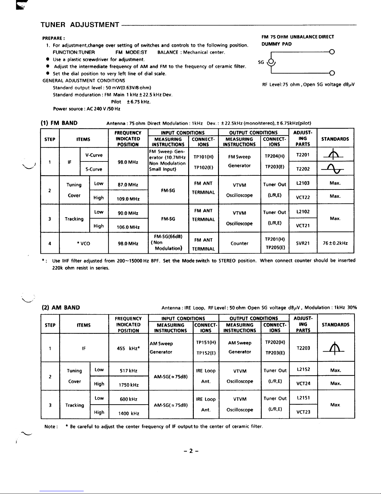
TUNER ADJUSTMENT
PREPARE :
FM 750HM UNBALANCE DIRECT
1. For adjustment, change oversetting of switches and controls to the following position.
DUMMY PAD
FUNCTION: TUNER
FM MODE:ST
BALANCE : Mechanical center.
● Use a plastic screwdriver for adjustment.
S.Y$O
●
Adjust the intermediate frequency of AM and FM to the frequency of ceramic filter.
● Set the dial position to very left line of dial scale.
GENERAL ADJUSTMENT CONDITIONS
Standard output level :50 mW(O.63V/8 ohm)
RF Level:75 ohm, Open SG voltage dB,uV
Standard moderation: FM Main 1 kHz * 22.5 kHz Dev.
Pilot * 6.75 kHz.
Power source: AC 240 V 150 Hz
(1)Fft
F
STEP
‘w) ‘
BAND Antenna :75 ohm Direct Modulation: 1kHz Dev.: t 22.5kHz (mono/stereo), f 6.7 Sk Hz(pilot)
FREQUENCY INPUT CONDITIONS OUTPUT CONI
ITEMS
INDICATED
MEASURING
CONNECT- MEASURING
POSITION INSTRUCTIONS
IONS INSTRUCTIONS
FM Sweep Gen-
V-Curve
erator (10.7 MHz
TP101(H)
FM Sweep
IF
98.0 MHz
Non Modulation
S-Curve Small Input)
TP102(E)
Generator
u--
Tuning
2
Cover
E
3
4
Tracking
FM-SG(66dB)
● Vco 98.0 MHz
( Non
FM ANT
Counter
Modulation)
TERMINAL
TP204(H)
I-=!!&&
TP203(E)
I
T2202
1+
‘“~’3=-l-
Tuner Out
H
L2 102
Max.
(UR,E)
VCT21
TP201(H)
SVR21
76~0.2kHz
TP205(E)
● : Use IHF filter adjusted from 200-15000 Hz BPF. Set the Mode switch to STEREO position. When connect counter should be inserted
220k ohm resist in series.
L,:
(2) AM BAND
Antenna : IRE Loop, RF Level: 50 ohm Open SG voltage d8,dJ, Modulation :1 kHz 30%
F
1
I
IF
Tuning
Low
2
Cover
High
Low
3
Tracking
High
I
AM Sweep
4S5 kHz*
Generator
=2-=
+ ‘“-sG(=75dB)
1400 kHz
I
IONS
OUTPUT CONDITIONS
ADJUST-
CONNECT-
MEASURING
CONNECT-
ING
STANDARDS
IONS
INSTRUCTIONS
IONS PARTS
IRE
LOOP
VTVM
Ant.
Oscilloscope
IRE
LOOfl
VTVM
Tuner Out
H
L2151
Max
Ant. Oscilloscope
(UR,E)
VCT23
Note:
● 8e careful to adjust the center frequency of IF output to the center of ceramic filter.
L
i
-2-
Page 4
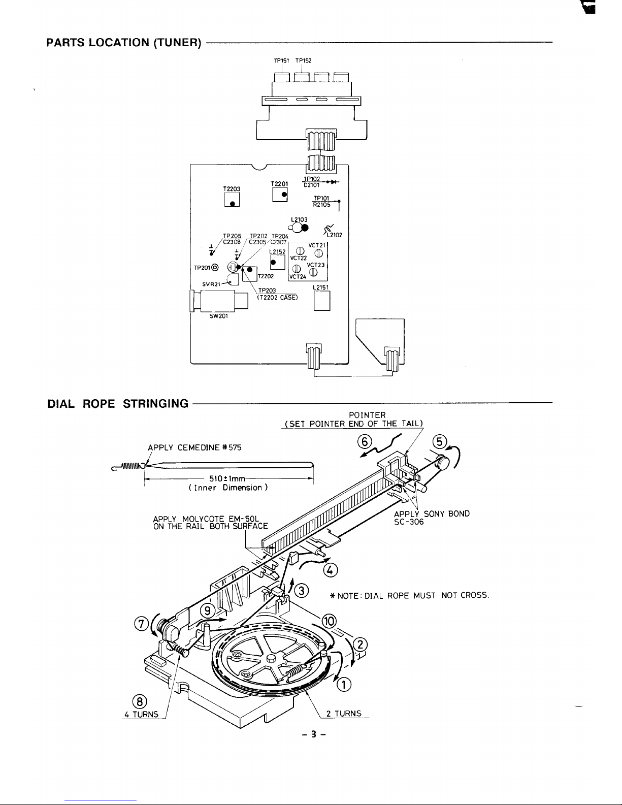
Fii
PARTS LOCATION (TUNER)
DIAL ROPE
TP151 TP152
e==+
—00—
r- ‘7
w
TP102
T2201
T2203
❑
mm-+
❑
+%
L2103
0 ,g,02
~<.d ,
‘ C23;P’= vc!!2vc~
TP201 @ i
,(2,vg3
T2202
SVR21
m “’2CASE) 0
SW201
lip
I
\
.-!F-
STRINGING
POINTER
(SET POINTER END OF THE TAIL)
APPLY CEMEDINE #575
3 Ah”
0/’
6
@
/
\
. Yl\
— 51021mm
I
( Inner Dimension )
-1
/A~+
BOND
+&@
-k NOTE : DIAL ROPE MUST NOT CROSS.
4 %NS / ~ \ 2 TURNS
-3-
Page 5
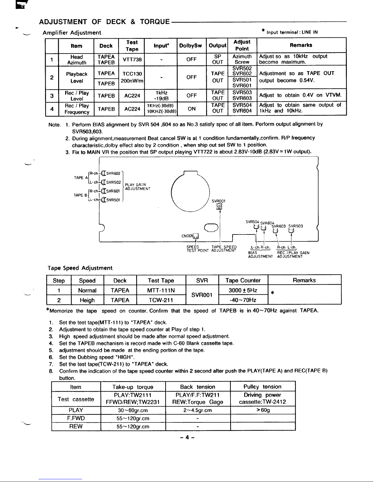
ADJUSTMENT OF DECK & TORQUE
Amplifier Adjustment
* lnputterminal: LINEIN
Item
Deck
Test
Input’
DolbySw output
Adjust
Tape
Point
Remarks
1
Head
TAPEA
VTT738 -
OFF
Azimuth
Adjust so as 10kHz output
Azimuth
TAPEB
OS(T
Screw
become maximum.
TAPEA TCC130
SVR502
2
Playback
OFF
TAPE
SVR602
Adjustment so as TAPE OUT
Level
TAPEB
200rrW/m -
OUT
SVR501
output become 0.54V.
SVR601
3
Rec / Play
TAPEB AC224
1kHz
Level
-19dB
OFF
y:; g:::; Adjust to obtain 0.4V on VTVM.
4
Rec I Play
TAPEB
lKHz(-30dB)
TAPE SVR504
Adjust to obtain same output of
Frequency
AC224 10KHZ(-30dB) ON OUT
SVR604
1kHz and 10kHz.
Note. 1.
2.
3.
Perform BIAS alignment by SVR 504,604 so as No.3 satisfy spec of all item. Perform output alignment by
SVR503,603.
During alignment, measurement Beat cancel SW is at 1 condition fundamentally,confirm. fUP frequency
characteristic, dolby effect also by 2 condition , when ship out set SW to 1 position.
Fix to MAIN VR the position that SP output playing VTT722 is about 2.83V-1 OdB (2.83V = 1W output).
[
R-ch ~SVR64)2 -
TAPE A
L- ch~SVR502
[1
R-ct4fsvR601
TAPE B
tiL-c~SVR501 ,
I
PLAY GA1 N
ADJUSTMENT
.0
SVROO1
?
+
I
a
CNOO
Q,
nfT0T03Y5
~~’
SPEED
TAPE SPEED
~-!~-~!~ch,
TEST POINT ADJUSTMENT
BIAS
REC /PLAY GAIN
ADJUSTMENT ADJUSTMENT
Tape Speed Adjustment
Step Speed
Deck
Test Tape
SVR
Tape Counter
Remarks
1 Normal TAPEA MTT-lll N 3000 ? 5Hz *
2 Heigh TAPEA
SVROO1
TCW-211
-40-70Hz
*Memorize the tape speed on counter. Confirm that the speed of TAPEB is in 40-70Hz against TAPEA.
1.
Set the test tape(MTT-111 ) to “TAPEA” deck.
2. Adjustment to obtain the tape speed counter at Play of step 1.
3. High speed adjustment should be made after normal speed adjustment.
4. Set the TAPEB mechanism is record made with C-60 Blank cassette tape.
5. adjustment should be made at the ending portion of the tape.
6. Set the Dubbing speed “HIGH”.
7. Set the testtape(TCW-211 ) to “TAPEA” deck.
8. Confirm the indication of the tape speed counter within 2 second after push the PLAY(TAPE A) and REC(TAPE B)
button.
Item Take-up torque Back tension
Pulley tension
Test cassette
PLAYTW211 1
PLAYIF.F:TW211
Driving power
FFWD/REW;TW2231
REW:Torque Gage cassette: TW-2412
PLAY
30-60gr.cm
2-4.5gr.cm
>
6(Jg
F.FWD 55-120gr.cm
REW
55-120gr.cm
-4-
Page 6

REPLACEMENT
OF HEADS
TAPE “B”
TAPE “A”
BROWN
WHITE
RE13
‘lN\K\ YELLOW \ /
FROM 6P CONNECTOR
BRO’WN
(FROM9P CONNECTOR)
RED
WHITE
FROM 9’P CONNECTOR BLACK
APPLVCEMEDINE TO FIX
APPLY CEMEDINETO FIX
SCHEMATIC DIAGRAM (TURN TABLE)
LG .
---------- ,
,
_________ .
RG’‘
(
L
I
CARTRIDGE
I
,1 ,
I ,1 ,
ADJ
USTM
33 RPM HOLE
FOR ADJUSTMENT
0
(a) 0
LEAF
SWITCH
MOTOR : MMI -6S2RWA0
Ii: 11:
kAA
lK(B)
45 Ipm
blw
CD MECHANISM
,. —
1)
1)
2)
3)
2)
1)
2)
3)
4)
‘-
5)
REMOVAL
Preparations
Do not apply unnecessary force to the pickup when handling it. Care should be taken not even to touch the lens or drive
circuit sections.
Do not apply unnecessary force (do not pull or push it forcefully) to remove the disc tray from its inside position.
Unnecessary force may break the teeth on the tray gear (CM6).
In the descriptions which follow, the numbers in the parentheses after the parts are reference numbers in the exploded
views. Refer to these views.
Removing and installing the disc tray
2-TH TOOTH
OF TRAY GEAR
Remove the stop screw (YI O) of the disc tray (17). (~)
Pull the disc tray (17) all the way forward by turning the
tray drive gear (CM12) clockwise. (~)
Note: Do not take hold of the disc tray (17) and pull it out by
force.
Push the catch on the disc tray (17) in the direction
shown by the arrow, and draw out the disc tray (17).
To install the disc tray, turn the gear (CM12) in the
direction of the arrow as far as it will go. (@)
Align the disc tray (17) with the mechanism chassis
(CM39).
6) Push the disc tray (17) toward the rear, and interlock it
L
/
///
7)
3)
(1)
1)
2)
‘L
3)
4)
5)
with the tray drive gear (CM I 2) as shown in Fig.@ .
Secure it with the screw (Yl O) which was removed in
step 1).
Disassemblingthe mechanism
Removing the pickup block
Remove the disc tray (17). (Refer to steps 1), 2) and 3)
of the section entitled “Removing and installing the disc
TRAY MOVE GEAR (CM) (CM,) TRAY GEAR
tray.”)
u
Turn the tray drive gear (CM12) counterclockwise (~),
and move the pickup in the direction of arrow (@) as far
as it will go.
Remove the spring wire (CM27) with tweezers. (@)
Remove the screw (CM11 ), and also remove the disc
tray (17) and washer (CM1 3). (@)
Now remove the pick rack gears (CM I 6 and CM1 9).
Note: It will not be possible to remove the pick rack gears
(CM16 and CM19) unless the pickup has been moved
all the way in the direction of arrow (@).
6) The pickup block can now be removed by taking out the
screw (CM51).
Note: If the timing gear (CM23) is in the state shown by “X”
in the figure on the right, put it in the state shown by
“o”.
‘L
F’
-6-
Page 8
‘mm! -
‘“
- --’”
Iii
—
MECHANISM REMOVAL (CD)
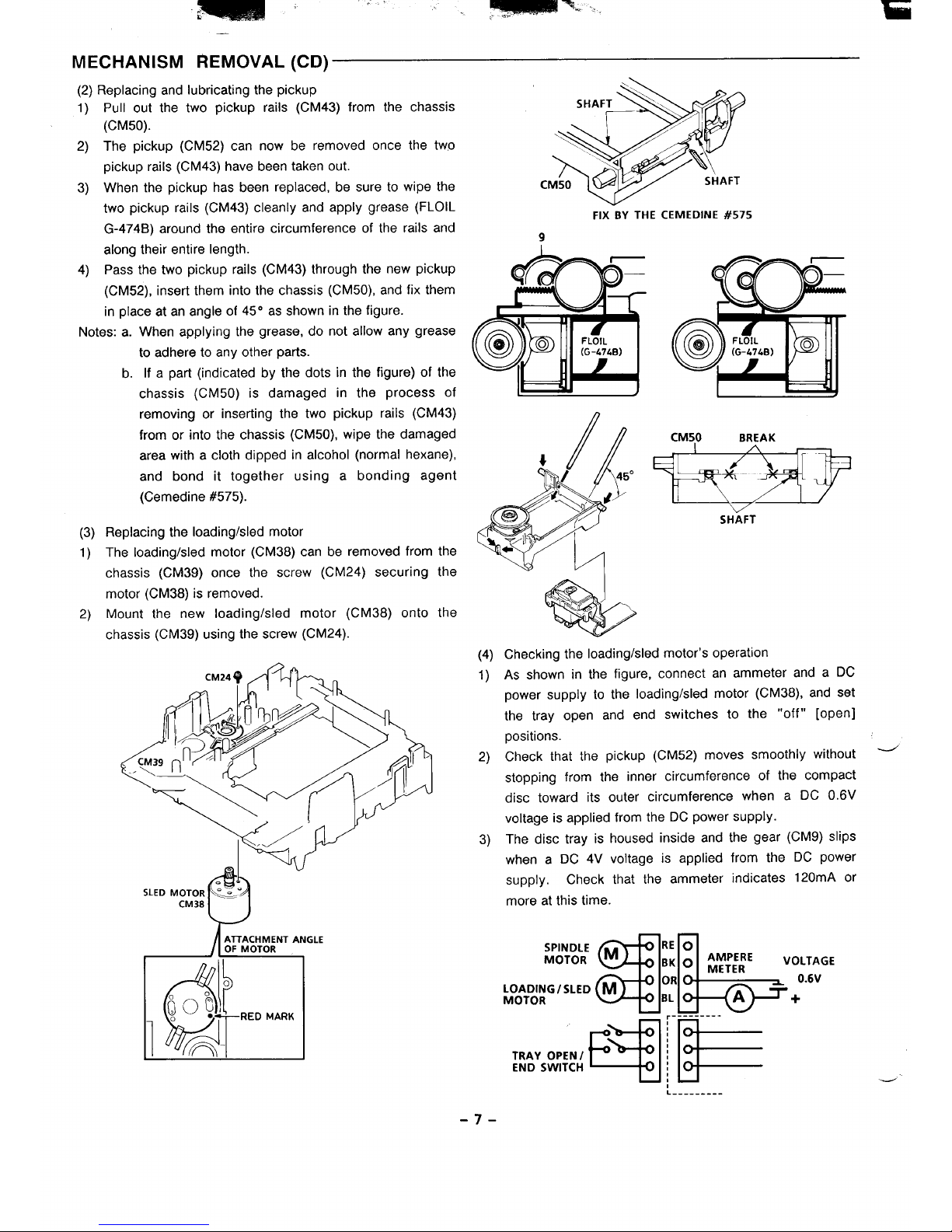
(2) Replacing and lubricating the pickup
‘<q
‘\
1) Pull out the two pickup rails (CM43) from the chassis
SHAFT ~
(CM50).
,/
@
2) The pickup (CM52) can now be removed once the tw,o
pickup rails (CM43) have been taken out.
3) When the pickup has been replaced, be sure to wipe the
crvl,rl & /
SHAFT
two pickup rails (CM43) cleanly and apply grease (FLOIL
G-474B) around the entire circumference of the rails and
FIX BY THE CEMEDINE #575
a
along their entire length.
4) Pass the two pickup rails (CM43) through the new pickup
@&e_
~c
(CM52), inserf them into the chassis (CM50), and fix them
in place at an angle of 45” as shown in the figure.
Notes: a. When applying the grease, do not allow any grease
m
o
@ o ,G-,,h,)
FLOIL
to adhere to any other parts.
b. If a part (indicated by the dots in the figure) of the
chassis (CM50) is damaged in the process of
removing or inserting the two pickup rails (CM43)
from or into the chassis (CM50), wipe the damaged
area with a cloth dipped in alcohol (normal hexane),
IL
and bond it together using a bonding agent
L/ 45°
(3)
1)
2)
(Cemedine #575).
e
,,.
#
/ #k
@?J >P-
Replacing the loading/sled motor
* [>
The loading/sled motor (CM38) can be removed from the
7 A
chassis (CM39) once the screw (CM24) securing the
motor (CM38) is removed.
Mount the new loading/sled motor (CM38) onto the
chassis (CM39) using the screw (CM24).
CM24 ?
CM38
In
ATTACHMENT ANGLE
OF MOTOR
.
~~
o
0 0.
O*
RED MARK
1 ‘% m-
(4)
1)
2)
3)
VI
SHAFT
Checking the loading/sled motor’s operation
As shown in the figure, connect an ammeter and a DC
power supply to the loading/sled motor (CM38), and set
the tray open and end switches to the “off” [open]
positions.
Check that the pickup (CM52) moves smoothly without stopping from the inner circumference of the compact
disc toward its outer circumference when a DC 0.6V
voltage is applied from the DC power supply.
The disc tray is housed inside and the gear (CM9) slips
when a DC 4V voltage is applied from the DC power
supply.
Check that the ammeter indicates 120mA or
more at this time.
——
-“
L---------
-7-
Page 9

m
MECHANISM REMOVAL (CD)
.—
4)
(1)
1)
2)
Check points for CD mechanism assembly and
lubrication
Lubricating and mounting the tray slide
Apply grease (FLOIL G-4748) to the area indicated by the
diagonal
in the figure.
When inserting the tray slide (CM1 5), set the position
where it is installed vis-a-vis the base/tray timing gear
(CM20) as shown in the figure.
y
P
BASE / TRAY
v I TIMING GEAR (CM20)
(3)
1)
2)
3)
4)
(2)
1)
2)
3)
Installing the tray gear
Move the tray slide (CM I 5) in the direction of the arrow
0.
Engage the gear section of the tray slide (CM15) with the
inner gear of the tray gear (CM6) at the center line, as
shown in the figure.
Align the tray move gear (CM3) with the position
(0) of
the hole in the outer gear of the tray gear (CM6), and
engage the tray move gear (CM3), as shown in the figure.
TRAY
SLIDE
CM6
Installing the base up/down slide and timing gear
Move the base up/down slide (CM14) in the direction of
the arrow @, and set the gears at the positions shown in
the figure.
Insert the timing gear (CM23), and mount it using the
screw (CM21 ).
Turn the timing gear (CM23) counterclockwise.
TIMING GEAR
BASE UP/ DOWN
@JF~:~4
\
v SCREW (CM21)
@
Hook the gear tension spring (CM22) onto the timing gear
(CM23).
msH’oN
-8-
Page 10
.
MECHANISM REMOVAL (CD)
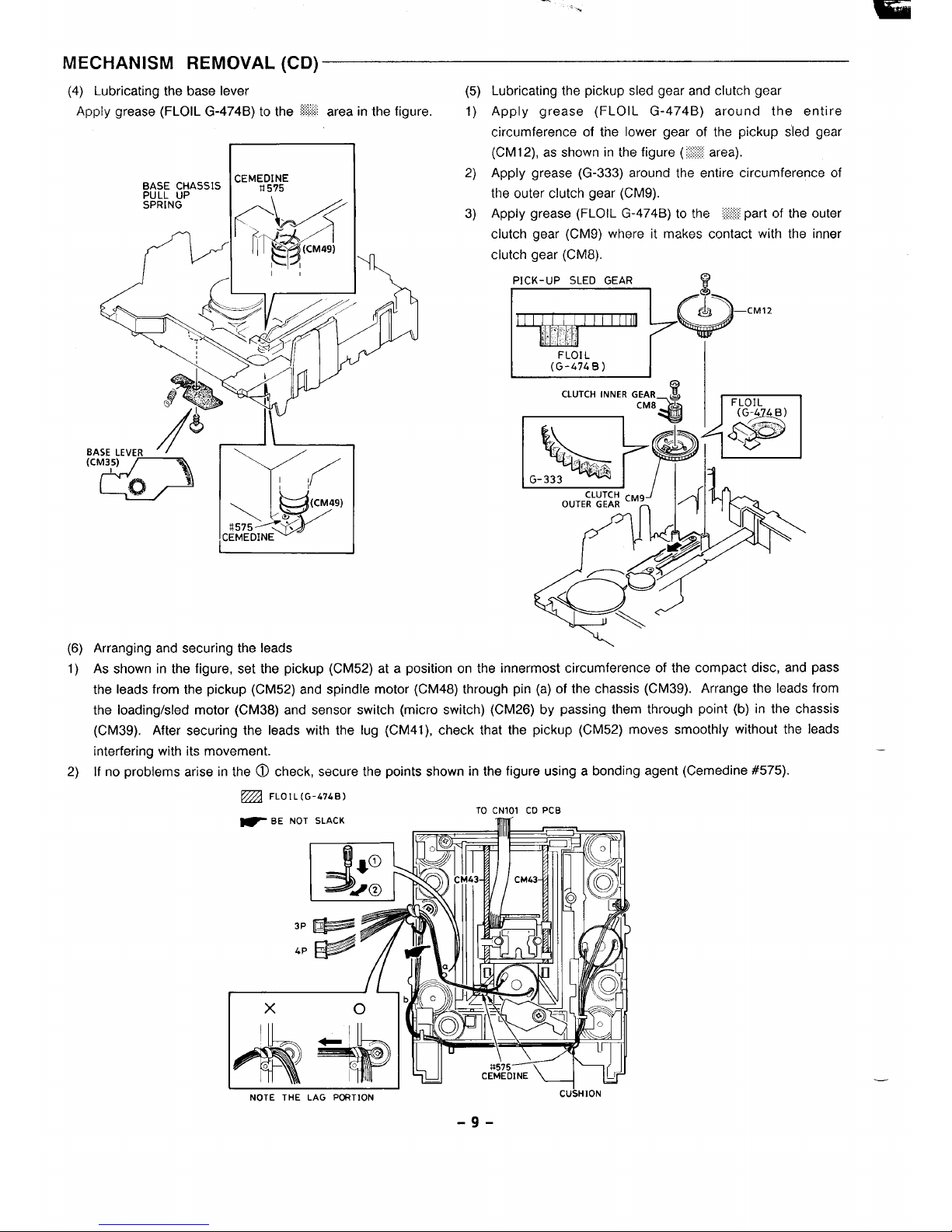
(4) Lubricating the base lever
(5)
Apply grease (FLOIL G-474B) to the ~~ area in the figure. 1)
2)
3)
1
I
(6) Arranging and securing the leads
Lubricating the pickup sled gear and clutch gear
Apply grease (FLOIL G-474B) around the entire
circumference of the lower gear of the pickup sled gear
(CM1 2), as shown in the figure (w area).
Apply grease (G-333) around the entire circumference of
the outer clutch gear (CM9).
Apply grease (FLOIL G-474B) to the ~ part of the outer
clutch gear (CM9) where it makes contact with the inner
clutch gear (CM8).
-CM12
L&h-l
I
CLUTCH INNER GEAR ~
~ ‘“84 w
pJ@._Jp,
p!??d
CLUTCH cM9~
OUTER GEAR n
k-w-oca
1) As shown in the figure, set the pickup (CM52) at a position on the innermost circumference of the compact disc, and pass
the leads from the pickup (CM52) and spindle motor (CM48) through pin (a) of the chassis (CM39). Arrange the leads from
the loading/sled motor (CM38) and sensor switch (micro switch) (CM26) by passing them through point (b) in the chassis
(CM39). After securing the leads with the lug (CM41 ), check that the pickup (CM52) moves smoothly without the
interfering with its movement.
2) If no problems arise in the @ check, secure the points shown in the figure using a bonding agent (Cemedine #575).
~ FLOIL(G-L7LB)
TO CN101 CO PCB
BE NO1
3P
4P
~L
o
+
lx
-3
1°
leads
.
.
CUkHION
NOTE THE LAG PORTION
-9-
Page 11
CD ADJUSTMENT
Electrical Adjustment
Preparations for Adjustments
So far we have presented explanations regarding compact
Measuring instruments, tools and filter
disc player handling, notes prior to repair, handling the pickup
(1)
Test disc. : YEDS 18 (Sony)
and disassembly of fhe unit. Be $w’e to carefully read these
(2)0sclllIwMpt3:SS5711 (1OMHZ or dua[ phenomenon)
instructions before making any adjustments.
or Memoryscope: DSS6521 (Storagescope)
r
Notes :a.
b.
c.
1.
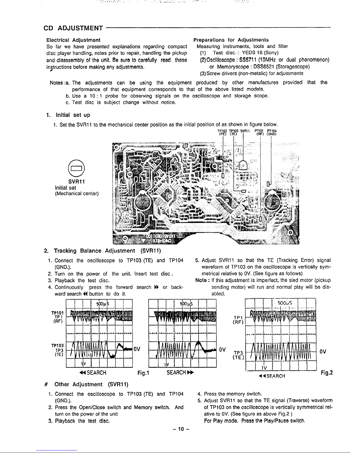
Initial
(3) Screw drivers (non-metalic) for adjustments
The adjustments can be using the equipment produced by other manufactures provided that the
performance of that equipment corresponds to that of the above listed models.
Use a 10:1 probe for observing signals on the
oscilloscopeand storage scope.
Test disc is subject change without notice.
set up
1. Set the SVR11 to the I
e
SVR1l
Initial set
(Mechanical center)
2. Tracking Balance Adjustment (SVR11)
1. Connect the oscilloscope to
TPI 03 (TE) and TP104
5. Adjust SVR11 so that the
TE (Tracking Error) signal
(GND.).
waveform of
TP103 on the oscilloscope is vertically sym-
2. Turn
on the power of the unit. Insert test disc .
metrical relative to OV. (See figure as follows)
3. Playback the test disc.
4. Continuously
press the forward
ward search ~ button to do it,
TP103
TP3
(TE)
Ov
Note: If this adjustment is imperfect, the sled motor (pickup
search N or back-
sending motor)
willrun and normal play will be dis-
abled.
44 SEARCH
Fig.1 SEARCH W
# Other Adjustment (SVR11)
Ov
TP1
(RF)
TP3
(TE)
44 SEARCH
Ov
F!g.2
1.
2.
3.
Connect the oscilloscope to TP103 (TE) and TP104
4.
Press the memory switch,
(GND.). 5. Adjust
SVR11 so that the TE signal (Traverse) waveform
Press the Open/Close switch and Memory switch. And of TP103 on the oscilloscope is vertically symmetrical relturn on the power of the unit ative to OV. (See figure as above Fig.2 )
Playback the test disc.
For Play mode. Press the Play/Pause switch,
-1o-
Page 12
i
,.
CONFiRM—--–
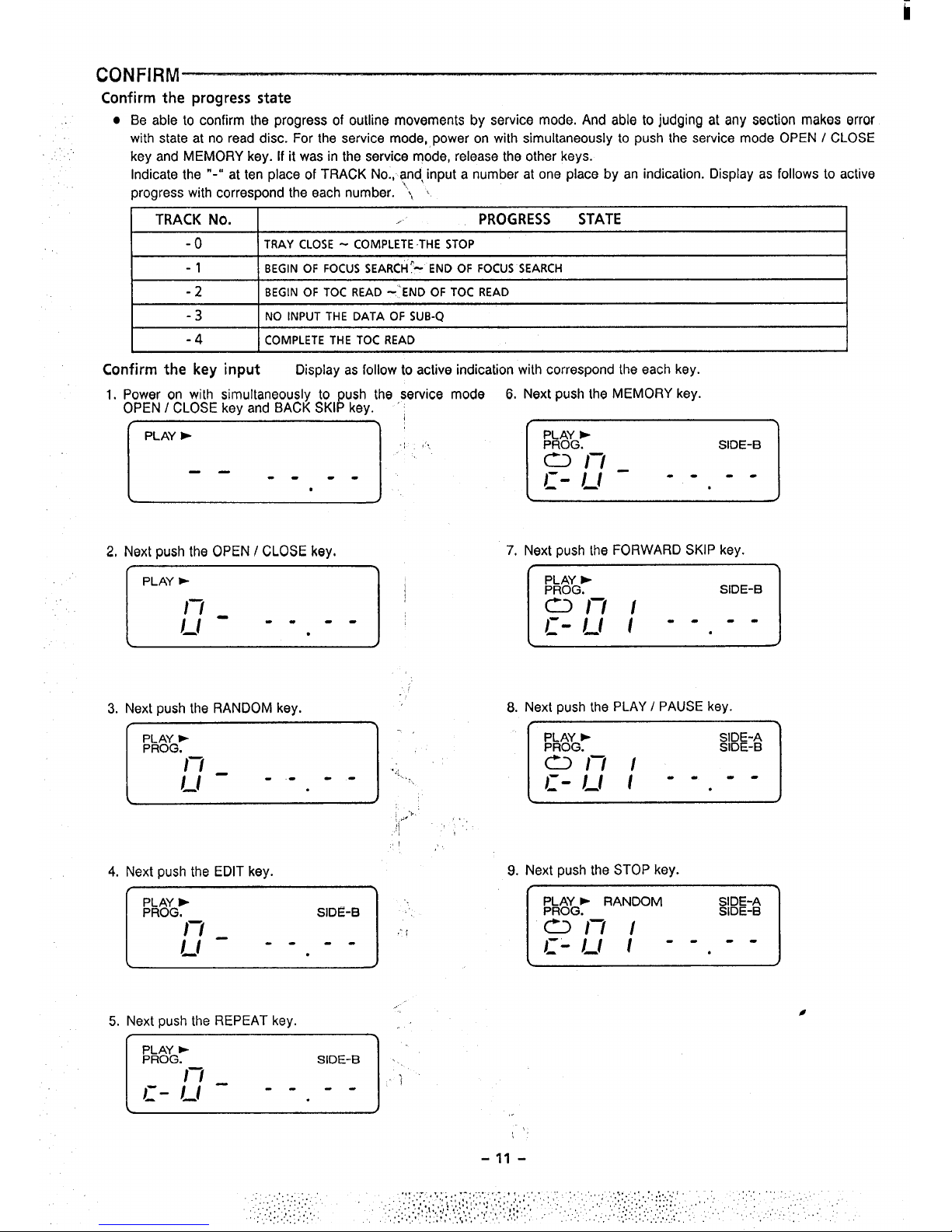
Confirm the progress state
. Be able to confirm the progress of outline movements by
service mode, And able to judging at any section makes error
with state at no read disc. For the service
mode, ,power on with simultaneously to push the service mode OPEN / CLOSE
key
and MEMORY key. If it was in the service mode, release the other keys.
Indicate the “-”
at ten place of TRACK No., and, input a number at one place by an indication. Display as follows to active
progress with correspond the each number. “i, \
TRACK
hlo.
.,
PROGRESS
STATE
I
-o
TRAY CLOSE- COMPLETETHE STOP
-1
BEGINOF FOCUSSEARCH!- END OF FOCUSSEARCH
i
J
-2
BEGIN OF TOC READ -“END OF TOC READ
-3 NO INPUT THE DATA OF SUB-Q
I
-4
COMPLETE THE TOC READ
I
Confirm the key input Display as follow to active indication with correspond the each key.
1.
2,
3.
4
Power on with simultaneously to ush the ,service mode
P
6. Next push the
MEMORY key.
OPEN / CLOSE key and BACK SKI key.
PLAY ●
--
---,
Next push the OPEN /
CLOSE key.
PLAY >
17 . . . . .
)_/
●
Next push the RANDOM key.
E
Next push the EDIT key.
I
.1 ,’.
1
.,
“...,.
,.,
,,
PLAY ➤
PROG,
SIDE-B
‘“
/–l ----- - I
)_l
●
5. Next push the REPEAT key.
PLAY *
PROG.
SIDE-B
I–l -----
c - I_!
.
7,
8.
PLAY >
PROG.
SIDE-B
es/-l_ -- .~- /_/
.
Next push the FORWARD SKIP key.
PLAY >
PROG.
SIDE-B
O//;l (....
~- _
.
Next push the PLAY I PAUSE key.
PLAY ➤
PROG.
SIDE-A
SIDE-B
y; /
~-_-.*--
9.
Next push the STOP key.
c
,.
-11-
Page 13

,.,
-,,,-,,,. ... . .,.,... .,
“,.:. ,’..:,,.,:’,., ..... .“, .
.: ..,..,
... , ,,, . . .
,.
., .,,.,. .
..’.. ,’.,’ ,’, .
,.:,’: . ....
., ...,
.,,
..... .....
..’.... .,. . . . . .
,.
. :.,.,....
EXPLODED VIEW (CABINET )
Uwl
/l!v
Y4
H
/“ ‘4
.
Y1
%)-Y1
-7
%-Yl
-12-
Page 14
ii
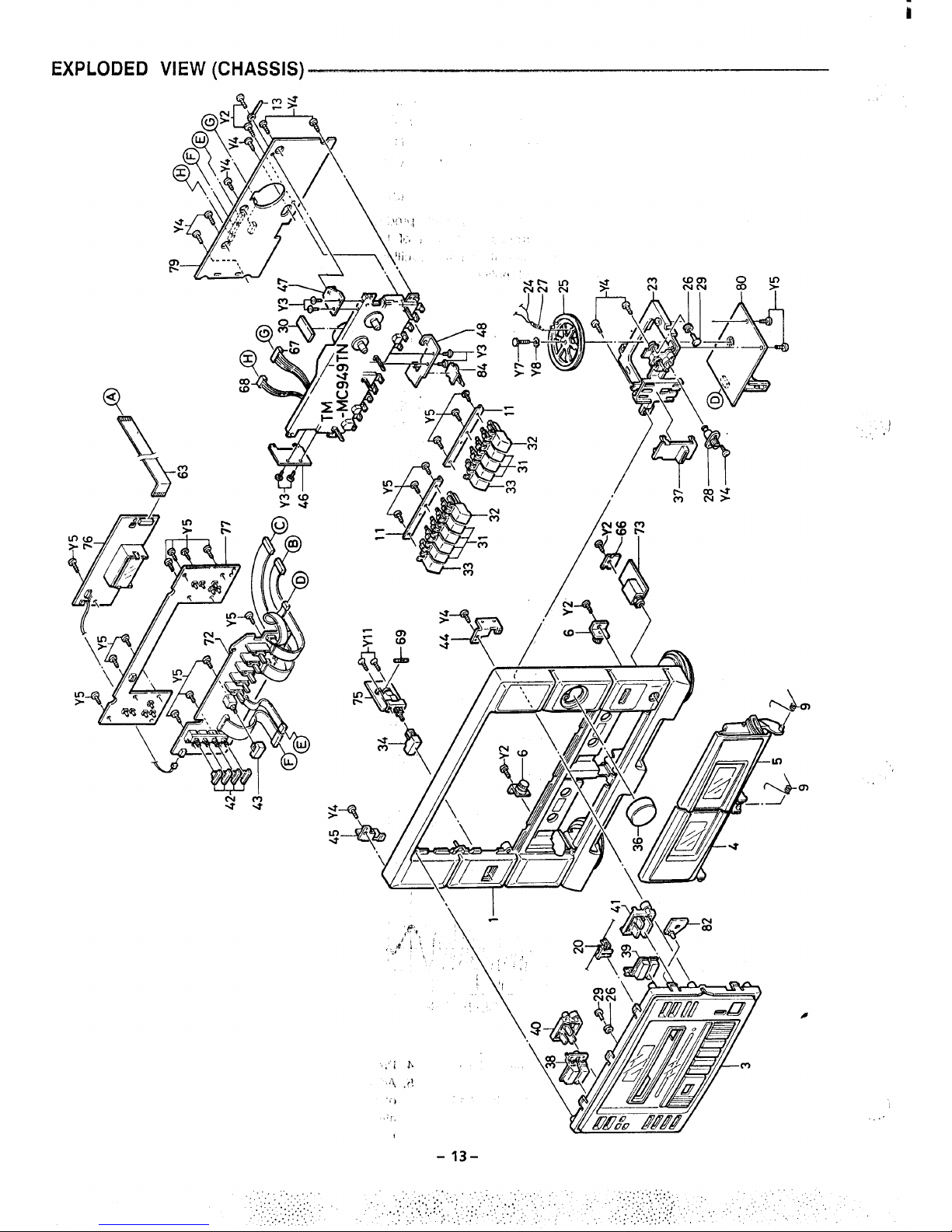
EXPLODED VIEW (CHASSIS) ~~
am
CyCy
-/1 /
-13-
“)
.,,,
m
..
Page 15

PARTS LIST
PRODUCT SAFETY NOTICE
Each precaution in this manual should be followed during servicing. Components identified with the IEC symbol ~ in the parts list
and the schematic diagram designate components in which safety can be of special significance. When replacing a component identified ~, use only the replacement parts designated, or parts with the same ratings of resistance, wattage or voltage that are designated in the parts list in this manual. Leakage-current or resistance measurements must be made to determine that exposed parts
are acceptably insulated from the supply circuit before returning the product to the customer.
CAUTION: Regular type resistors and capacitors are not list. To know those values, refer to the schematic diagram.
~BINET
Ref. No.
1
2
3
4
5
6
7
8
9
10
11
12
13
14
or
15
16
17
18
19
20
21
22
23
24
25
26
27
28
29
30
31
32
33
k ACCESSORIES
Part No.
614 246 1198
614 246 1204
614 240 6656
614 240 6663
614 176 7024
614 246 1211
614 231 6832
614 224 3480
614 245 9348
614 234 5511
614 232 6671
i CHASSIS
Part No.
614 246 1112
614 230 5096
614 246 1129
614 241 5504
614 241 5528
614 069 0385
614 239 4403
614 239 4410
614 216 0051
614 239 4281
614 194 9239
614 216 7083
614 130 0382
614 243 4109
614 246 1136
614 129 1901
614 240 2726
614 238 1694
614 242 2403
614 195 6976
614 240 2665
614 240 2702
614 240 2719
614 240 2771
614 118 5590
614 132 2773
614 135 5702
614 146 8778
614 068 7972
614 240 7716
614 208 0986
614 216 9063
614 216 9117
614 216 9124
Description
INNER CARTON “SINGAPORE”
INNER CARTON “MALAYSIA”
PAD,BOTTOM
PAD,TOP
INNER POLYE COVER,SET
INSTRUCTION MANUAL
LABEL,SAFETY,LASER CLASS
INDICATE
LABEL,NEEDLE(ST-707J)
SHEET,CD TRAY
LOOP ANTENNA,AM ANT
ANTENNA,FM ANT
Description
!SSY,PANEL,FRONT
?ANEL,Tf)p,TIJR$J TABLE
V3SY,PANEL
4SSY,LID,CASSETTE,TAPE B
USSY,LID,CASSETTE,TAPE A
2EAR ASSY
PANEL,SIDE,R
PANEL,SIDE,L
5PRING,WIRE,LID CASSETTE
CABINET,BOTTOM
BRACKET,MECHA KNOB
4SSY,FOOT
LUG,DECK PCB(DRESS LEAD)
PANEL,REAR “SINGAPORE”
PANEL,REAR “MALAYSIA”
FIXER,AC CORD
BRACKET-M,CD MECHA
TABLE,LOADING,CD TRAY
ESCUTCHEON,CD TRAY
RUBBER CUSHION,CD MECHA
POINTER
BRACKET-M,CD MECHA
(R)
BRACKET-M,CD MECHA
(L)
MOUNT-M,TUNER PCB
ROPE O.3X11OOMM
DRUM
PULLEY
SPRING COIL,ROPE
TUNING SHAFT ASSY
PIN,PULLEY
CUSHION,MECHA LEAD
BUTTON,MCHA BUTTON
(STOP,ETC)
BRACKET
BRACKET
FIX
BUTTON,MECHA (PAusE)
BUTTON,MECHA (REC,ETC)
Ref. No.
34
35
36
37
38
39
40
41
42
43
44
45
46
47
48
49
,1
,2
br
13
14
Part No.
614 239 4519
614 228 0218
614 240 2634
614 240 2641
614 242 0430
614 242 0423
614 240 2351
614 239 4557
614 240 236B
614 240 2656
614 239 4618
614 240 6926
614 216 9230
614 216 9247
614 216 9254
614 212 6343
614 219 6223
614 234 1056
614 234 3692
614 112 3479
614 112 3486
‘IXING PARTS
Ref. No.
Y1
Y2
Y3
Y4
Y5
Y6
Y7
Y6
Y9
Ylo
Yll
Y12
Y13
Part No.
411 021 6603
411 021 3503
411 028 2905
411 021 6405
411 021 1806
411 001 3905
411 011 4503
411 085 1200
411 021 1202
411 022 6406
411 022 2802
412 032 6408
412 004 5705
Description
BUTTON,POWER
BUTTON,DUBBING,BEAT CCL
KNOB,ROTARY,TUNER
KNOB,SLIDE,BAND
BUTTON,REPEAT.MEMORY
BUTTON,PLAY/STOP
BUTTON,EDIT.RANDOM INTRO
BUTTON,SKIP.OPEN.CLOSE
BUTTON,CD/TU/TAPE/PHONO
BUTTON,BASSXPANDER
BRACKET-E,FRONT-SIDE (R)
BRACKET-E,FRONT-SIDE (L)
BRACKET-E,DECK PCB
BRACKET-E,OECK PCB
BRACKET-E,DECK PCB
LABEL,SAFETY,LASER
ASSY,COVER,OUST
ASSY SHEET TURNTABLE
ASSY SHEET TURNTABLE
HINGE,R
HINGE,L
Description
SCR S-TPG BIN
3X8,PANEL,SIDE & TOP
SCR S-TPG BIN 3X1O
SCR S-TPG PAN 2X4,DECK
BRACKET-E
SCR S-TPG
BIN 3X6
SCR S-TPG BIN 2.6X1O
SCR S-TPG BIN 4X6,TRANS
BOLT HEX C-SCT 2.6X16,DRUM
WASHER OUT TW 2.6,DRUM
SCR S-TPG BIN 2X8,TRAY
ESCUTCHEON
SCR S-TPG PAN 2X8,CD TRAY
STOPPER
SCR S-TPG FLT 3X1O,POWER SW
SPECIAL SCREW,PLAYER
SPECIAL SCREW,CD MECHA
FIX
ELECTRICAL PARTS
Ref. No. Part No. Description
61
~614 023 2912
POWER
CORD
62
~614 241 6365
POWER TRANS
63 614 240 8391
CORD,MECHA-MICON 14P
-14-
Page 16

Iiiz
PARTS LIST
Ref. No.
Part No.
64 614 243 9548
65
66
67
68
69
MAIN P.
Ref. No.
71
C4703
C4803
CN107
CN901
CN902
CN905
CN906
CN907
CN924
Dill
or
D112
or
D113
or
D114
or
D115
D4900
or
D4901
or
D4903
or
D4904
or
D4905
or
D4906
or
D4907
or
D4908
or
IC107
IC900
or
or
or
IC901
or
or
or
IC903
IC904
Q106
R4706
R4806
S4403
/h614 242 3844
h614 242 3851
614 218 6442
614 218 6459
~423 016 9308
BOARD ASSY
Part No.
614 242 3424
403 057 3800
403 057 3800
614 017 2591
614 020 6579
614 020 6555
614 017 2591
614 017 2607
614 020 6593
614 020 1246
Lh407 004 9105
A407 012 3300
A407 004 9105
A407 012 3300
A407 004 9105
A407 012 3300
A407 004 9105
A407 012 3300
407 007 9904
A407 004 9105
A407 012 3300
A407 004 9105
A407 012 3300
A407 004 9105
A407 012 3300
A407 004 9105
A407 012 3300
A407 004 9105
A407 012 3300
A407 004 9105
A407 012 3300
A407 004 9105
A407 012 3300
A407 004 9105
A407 012 3300
409 018 5500
h409 001 7603
h409 078 2402
h409 122 6202
~409 168 2107
d409 001 7603
h409 078 2402
h409 122 6202
~409 168 2107
409 017 7505
409 016 7902
405 082 4609
A401 015 6108
A401 015 6108
614 240 8759
Description
ASSY,CONNECTOR-S,MECHA-DG
8P
PCB,PT 1
PCB,HEADPHONE STOPPER
ASSY,CONNECTOR-S,6P
ASSY,CONNECTOR-S,3P
FUSE 250V 0.2A
Description
ASSY,PCB,MAIN
POLYESTER
O.lu M 50V
POLYESTER
O.lU M 50V
PLUG,TO CD MECHA,3P
SOCKET,HP,5P
SOCKET,3P
PLUG,PRI,8P
PLUG,PRI,9P
SOCKET,AC,7P
SOCKET,5P
DIODE DSF1OC
DIODE 1SR35-200A
DIODE DSF1OC
DIODE 1SR35-200A
DIODE DSF1OC
DIODE 1SR35-200A
DIODE DSF1OC
DIODE 1SR35-200A
DIODE GMAO1
DIODE DSF1OC
DIODE 1SR35-200A
DIODE DSF1OC
DIODE 1SR35-200A
DIODE DSF1OC
DIOOE 1SR35-200A
DIODE DSF1OC
DIODE 1SR35-200A
DIODE DSF1OC
DIOOE 1SR35-200A
DIODE DSF1OC
DIODE 1SR35-200A
DIODE DSF1OC
DIODE 1SR35-200A
DIODE DSF1OC
DIODE 1SR35-200A
IC LA651O
IC AN7812F
IC L7812ML
IC NJM7812FA
IC UPC7812HF
IC AN7812F
IC L7812ML
IC NJM7812FA
IC UPC7812HF
IC LA4270
IC LA3161
TR DTA123YS
CARBON 2.2 JB l/4W,FLAME
PROOF
CARBON 2.2 JB l/4W,FLAME
PROOF
SWITCH,PUSH, DUB/BEAT SW
Ref. No.
iRAPHIC
Ref. No.
12
;N911
:N912
:N914
:N915
:N916
:N917
)4402
)4501
j4502
]4601
?4602
?4406
?4407
34400
$4401
JR900
JR901
JR902
JR903
L/R904
Part No. Description
614 203 7362 HEAT SINK, l.5T
614 241 5863 HEAT SINK,2T
614 244 9639 ASSY,CONNECTOR-S,5P 300MM
411 021 6405 SCR S-TPG BIN 3X8,1C-HEAT
SINK
411 021 6405 SCR S-TPG BIN 3X8,AMP PCB-
HEAT SINK
EQUALIZER P.C.9
Part No.
614 242 3431
614 020 6579
614 020 6616
614 035 4980
614 035 4973
614 020 6562
614 017 3819
407 007 9904
405 012 2002
405 012 2002
405 012 2002
405 012 2002
401 058 3201
401 063 0608
614 240 8773
614 240 8780
614 240 9893
614 240 9893
614 240 9893
614 240 9909
614 240 9916
614 244 0155
614 244 1947
614 211 3202
614 245 7771
614 245 7788
HEADPHONE P.C.BOARDASSY
IARD ASSY
Descrir)tion
ASSY,PCB,GEQ
SOCKET,5P
SOCKET,9P
SOCKET,9P
SOCKET,8P
SOCKET,4P
PLUG,2P
DIODE GMAO1
TR 2SC1815-GR
TR 2SC1815-GR
TR 2SC1815-GR
TR 2SC1815-GR
OXIDE-MT
100
JA
OXIDE-MT
68 JA
SWITCH,PUSH,FUNCTION
SWITCH, PUSH,BASS.EXP .
VR,SLIDE,GEQ
VR,SLIDE
VR,SLIDE
VR,SLIDE,BALANCE
VR,SLIDE,MAIN
lW
lW
SOCKET,TO DECK,9P(CN912CN718)
SOCKET,TO TUNER,4P(CN916CN203)
SOCKET,TO DECK,5P(CN911CN717)
ASSY,CONNECTOR-S ,TO
MAIN,CN915
ASSY,CONNECTOR-S,TO
MAIN,CN914
Ref. No.
73
CN920
CN921
Part No.
614 242 3448
614 020 6579
614 035 1712
Descri~tion
ASSY, PCB,HEADPHONE
SOCKET,TO MAIN,5P
SOCKET,H.P W/SW
PT SECONDARY P.C.BOARDASSY
Ref. No. Part No.
Description
74
614 242 3455
ASSY,PCB,PT SECONDARY
CN918
614 020 6593 SOCKET,C0,7P
614 129 9099 LUG
J’
.-.-’-
.15-
Page 17

PARTS LIST
POWER SWITCH P.C. BOARD ASSY
! Ref. No. I
Part No.
I
De$crbtion
75
C4922
or
S4404
614 242 3516
lh404 033 3401
h404 000 1607
~614 018 8967
Lh614 208 4540
h614 123 2089
LfJ614017 8203
ASSY, PC8, POWER Sw
CERAMIC O,OIU Z CERAMIC O,OIU F 400V
SWITCH
FUSE HOLDER
TERMINAL
TERMINAL BOARD
;D MICO
Ref. No.
76
CN106
CN108
CN132
D103
or
D104
or
IC108
LCDO1
PL101
Q103
Q104
Q11O
X102
or
:D SWIT
Ref. No.
77
CN109
Slol
S102
S103
S104
S105
S106
S107
S109
Silo
S1ll
I
P.C.BOARDASS
Part No.
614 242 3493
614 227 7942
614 243 9845
614 243 9555
407 007 9904
407 012 4406
407 007 9904
407 012 4406
410 147 9109
614 240 8193
614 045 9647
405 011 8609
405 000 4407
405
011 8609
614 215 5523
614 215 5561
614 240 8292
614 230 7359
614 232 0242
H P.C.BOARD A!
Part No.
614 242 3509
614 221 9041
614 220 5655
614 220 5655
614 220 5655
614 220 5655
614 220 5655
614 220 5655
614 220 5655
614 220 5655
614 220 5655
614 220 5655
I
Description
ASSY,PCB,CD-MICOM
SOCKET,14P
PLUG,TO SW
ASSY,CONNECTOR-S,2P
DIODE GMAO1
DIODE 1SS133
DIODE GMAO1
DIODE 1SS133
IC CXP5078H-523Q
LCD
LAMP,12V lOOMA
TR 2SC1740S-S
TR DTC124ES
TR 2SC1740S-S
RESONATOR,CERAM,4, 19MHZ
RESONATOR,CERAM
SHEET,ORANGE
MOUNT-E
SHEET
;Y
Description
ASSY,PCB,CD-SW
SOCKET,FROM
MICON
SWITCH,TACT,MEMORY
SWITCH,TACT,BACK
SWITCH,TACT,FWD
SWITCH,TACT,PLAYiPAUSE
SWITCH,TACT,STOP
SWITCH,TACT,OPENiCLOSE
SWITCH,TACT,RANOOM
SWITCH,TACT,EDIT
SWITCH,TACT,REPEAT
SWITCH,TACT,INTRO
;PEAKER TERMINAL P.C.BOARD ASSY
m
Descrir)tion
ASSY,PCB,SP TERMINAL
SOCKET,3P
TERMINAL,SP,4P W/SHIELD
DECK P.C.BOARD ASSY
Ref. No.
Part No.
Description
79
614 242 48m
lAssy,PcB,DEcK
C985
403 081 1209 POLYPRO
0.018U J 100V
CNOO1
614 017 2102
PLUG,AUTO TAPE,3P
Ref. No.
Part No. Description
;NO02 614 017 2133 PLUG,MECHA,6P
;NO05 614 016 4084 PLUG,HIGH SPEED,2P
:NO06 614 020 8849 SOCKET,TAPE 0UT,3P
;NO07 614 020 6562 SOCKET,MOTOR,4P
:NO08 614 020 6548 SOCKET,STOP SW,2P
;NO09 614 223 0329
ASSY,CONNECTOR-S,A MECHA,4P
W/LEAD
:NO1O 614 223 0336 ASSY,CONNECTOR-S,B MECHA,7P
W/LEAD
;N717
614 017 2126
PLUG,AMP1,5P
;N718 614 017 2164
PLUG,AMP2,9P
)001
407 007 9904 DIODE GMAO1
>r
407 012 4406 DIODE 1SS133
)002 407 007 9904 DIODE GMAO1
)r
407 012 4406 DIODE 1SS133
)003 407 007 9904
DIODE GMAO1
or
407 01? 4406 DIODE 1SS133
)004
407 007 9904 DIODE GMAOI
>r
407 012 4406 DIODE 1SS133
1005
407 007 9904
DIODE GMAO1
>r
407 012 4406 OIODE 1SS133
)006
407 007 9904 DIODE GMAO1
~r
407 012 4406
DIOOE 1SS133
JO07
407 007 9904
DIODE GMAO1
Dr
407 012 4406 DIODE 1SS133
DO08
407 007 9904 DIODE GMAO1
c)r
407 012 4406 DIODE 1SS133
DO09
407 007 9904 DIODE GMAO1
or
407 012 4406 DIODE 1SS133
DOlO
407 007 9904
DIODE GMAO1
or
407 012 4406 DIODE 1SS133
DO1l
407 007 9904
DIODE GMAO1
or
407 012 4406 DIODE 1SS133
D012
407 007 9904 DIODE GMAO1
or
407 012 4406 DIODE 1SS133
D013
407 007 9904
DIODE GMAO1
or
407 012 4406 DIODE 1SS133
D014
407 007 9904
DIODE GMAO1
or
407 012 4406 DIODE 1SS133
D015
407 005 4505 DIODE DS442X
or
407 013 7109 DIODE 1S2473
D016
407 007 9904
DIODE GMAO1
or
407 012 4406
DIODE 1SS133
D017
407 007 9904
DIODE GMAO1
or
407 012 4406
DIODE 1SS133
D018
407 007 9904
DIODE GMAO1
or
407 012 4406 DIODE 1SS133
D019
407 007 9904
DIODE GMAO1.
or
407 012 4406
DIODE 1SS133
D099
407 007 9904
DIODE GMAO1
or
407 012 4406
DIODE 1SS133
D501
407 007 9904
DIODE GMAO1
or
407 012 4406
DIODE 1SS133
D502
407 007 9904
DIODE GMAO1
or
407 012 4406
DIODE 1SS133
D601
407 007 9904
DIODE GMAO1
or
407 012 4406
DIODE 1SS133
D602
407 007 9904
DIODE GMAO1
or
407 012 4406
DIODE 1SS133
0
ICOO1
409 020 9107 IC LC4069UB
or
409 051 3907 IC TC4069UBP
or
409 059 3206 IC UPD4069UBC
IC501
409 121 8702
IC LA3246
IC502
409 145 8405
IC UPC1330HA
IC521
409 016 870 1 IC LA3220
IC551
409 119 980
3 IC CXA1101P
Page 18

PARTS LIST
Ref. No.
L501
L502
or
L511
L512
L601
L602
or
L611
L612
L981
QOO1
;;02
;:03
or
;:04
;;05
or
$06
;;08
or
;:09
or
;:10
or
::01
or
:;02
or
::04
or
:;05
or
;;06
or
;;07
or
;;08
or
:;09
or
;;10
or
;:01
or
or
Part No.
614 029 3807
614 027 8546
014 210 3685
614 202 8865
614 029 3142
614 029 3807
614 027 8545
614 210 3685
614 202 8865
614 029 3142
614 212 0804
405 001 7001
405 005 2002
405 001 7001
405 005 2002
405
011 8609
405 012 2002
405 020 7204
405 001 7001
405 005 2002
405
011 8609
405 012 2002
405 020 7204
405 012 7403
405 013 1301
405 011 8609
405 012 2002
405 020 7204
405 011 8609
405 012 2002
405 020 7204
405 011 8609
405 012 2002
405 020 7204
405 011 8609
405 012 2002
405 020 7204
405 011 8609
405 012 2002
405 020 7204
405 011 8609
405 012 2002
405 020 7204
405 011 8609
405 012 2002
405 020 7204
405 011 8609
405 012 2002
405 020 7204
405 011 8609
405 012 2002
405 020 7204
405 011 8609
405 012 2002
405 020 7204
405 011 8609
405 012 2002
405 020 7204
405 011 8609
405 012 2002
405 020 7204
405 011 8609
405 012 2002
405 020 7204
Description
MX
COIL
CHOKE 3,3UH
INDUCTOR,FERITE
FILTER 6,8MH
MX
COIL
MX COIL
CHOKE
INOUCTOR,FERITE
FILTER
MX
COIL
TRANS,OSC
TR 2SA1015-GR
TR 2SA733-P
TR 2SA1015-GR
TR 2SA733-P
TR 2SC1740S-S
TR 2SC1815-GR
TR 2SC945A-K
TR 2SA1015-GR
TR 2SA733-P
TR 2SC1740S-S
TR 2SC1815-GR
TR 2SC945A-K
TR 2SC2001-K
TR 2SC2120-Y
TR 2SC1740S-S
TR 2SC1615-GR
TR 2SC945A-K
TR 2SC1740S-S
TR 2SC1815-GR
TR 2SC945A-K
TR 2SC1740S-S
TR 2SC1815-GR
TR 2SC945A-K
TR 2SC1740S-S
TR 2SC1815-GR
TR 2SC945A-K
TR 2SC1740S-S
TR 2SC1815-GR
TR 2SC945A-K
TR 2SC1740S-S
TR 2SC1815-GR
TR 2SC945A-K
TR 2SC1740S-S
TR 2SC1815-GR
TR 2SC945A-K
TR 2SC1740S-S
TR 2SC1815-GR
TR 2SC945A-K
TR 2SC1740S-S
TR 2SC1815-GR
TR 2SC945A-K
TR 2SC1740S-S
TR 2SC1815-GR
TR 2SC945A-K
TR 2SC1740S-S
TR 2SC1815-GR
TR 2SC945A-K
TR 2SC1740S-S
TR 2SC1815-GR
TR 2SC945A-K
TR 2SC1740S-S
TR 2SC1815-GR
TR
2SC945A-K
Ref. No.
Part No. Description
Q602 405
011 8609 TR 2SC1740S-S
or
405 012 2002 TR 2SC1815-GR
405 020 7204 TR 2SC945A-K
;;04 405
011 8609
TR 2SC1740S-S
or 405 012 2002 TR 2SC1815-GR
405 020 7204’ TR 2SC945A-K
;;05
405 011 8609
TR 2SC1740S-S
or 405 012 2002 TR 2SC1815-GR
405 020 7204 TR 2SC945A-K
;;06 405 011 8609 TR 2SC1740S-S
or
405 012 2002 TR 2SC1815-GR
405 020 7204 TR 2SC945A-K
:;07 405
011 8609 TR 2SC1740S-S
or
405 012 2002 TR 2SC1815-GR
405 020 7204 TR 2SC945A-K
;;08
405
011 8609 TR 2SC1740S-S
or 405 012 2002 TR 2SC1815-GR
405 020 7204 TR 2SC945A-K
;;09 405
011 8609 TR 2SC1740S-S
or 405 012 2002 TR 2SC1615-GR
405 020 7204 TR 2SC945A-K
;;81
405 012 2002 TR 2SC1815-GR
405 020 7204
TR 2SC945A-K
;;82 405
011 8609 TR 2SC1740S-S
or 405 012 2002 TR 2SC1815-GR
405 020 7204 TR 2SC945A-K
;;83 405 012 2002 TR 2SC1815-GR
405 020 7204 TR 2SC945A-K
:i84 405
011 8609 TR 2SC1740S-S
or
405 012 2002 TR 2SC1815-GR
405 020 7204 TR 2SC945A-K
;;85 405
011 1907 TR 2SC1627-Y
Svool 614 204 1871 SEMI V,R,2K
SV501 614 003 6183 SEMI V,R,1OK
SV502 614 003 6183 SEMI V.R,1OK
SV503
614 003 6183 SEMI V.R,1OK
SV504 614 003 6237 SEMI V.R,200K
SV601 614 003 6183 SEMI V.R,1OK
SV602 614 003 6183 SEMI V,R,1OK
SV603 614 003 6183 SEMI V.R,1OK
SV604
614 003 6237 SEMI V.R,200K
&614 130 6926 TUBE, FOR R981 20X2
TUNER MAIN P.C.BOARD ASSY
Ref. No. Part No. Description
60
614 245 9447 ASSY,PCB,TU MAIN
C231O
403 080 8902 POLYPRO 1500P J 100V
CF201
614 030 5630 IF
FILTER,REO
or 614 030 5647
IF FILTER,BLUE
or 614 030 5654 IF FILTER,ORANGE
or 614 030 5661 IF FILTER,BLACK
or
614 030 5678 IF FILTER,WHITE
CF203
614 030 5197 IF FILTER,455KHZ
CN201
614 020 6579 SOCKET*5P
CN202
614 020 6548 SOCKET*2P
CN203
614 017 2263 PLUG,4P
02101 407 012 4406 DIOOE 1SS133
407 007 9904 DIOOE GMAO1
:;301 407 012 4406 DIOOE 1SS133
or
407 007 9904 DIOOE GMAO1
F2101
614 228 4704
FILTER,LC
IC201
409 049 2103 IC TA7358P
i
-17-
Page 19

..,, .,,..:.... .
,., ,,..,.
,’.
.. :...,.
PARTS LIST
Ref. No.
IC202
L2102
L2103
L2151
L2152
SVR21
SW201
T2201
T2202
T2203
TP201
VC201
Part No.
409 163 3802
814 034 e74g
614 035 0012
0
614 221 6814
614 034 1638
614 204 1901
614 239 7343
614 030 4091
614 030 3742
614 030 3803
614 017 6964
614 239 2416
Description
IC LA1805-SS
VHF
COIL
VHF COIL
TRANS,RF
O.S.C
COIL
SEMI
V,R,1OK
SWITCH,SLIDE
I.F,T,FM
I.F.T,FM
I.F,T,AM
+,,
TERMINAL BOARD
Vc
ANTENNA P.C.BOARD ASSY
Ref. No.
Part No.
I
Description
81
I
614 245 94541 ASSY,PCB.ANT
CN211 614 020 6579 SOCKET,5P
CN213 614 239 1686 TERMINAL,4P
LED P.C.BOARDASSY
Ref. No.
Part No.
82
614 245 9461
CN212 614 020 6548
D2401
408 014 6504
Description
ASSY,PCB,LED
SOCKET,2P
LED SLZ-138B-17-T1
:D MAII
Ref. No.
83
CN101
CN102
CN103
CN104
CN105
IC101
IC102
IC104
IC105
Q101
Q102
Q105
Q106
Q107
SVR1l
TP101
TP102
TP103
TP104
TP105
Xlol
P.C.BOARDASSY
Part No.
614 240 7967
614 227 7935
614 017 3833
614 017 3826
614 227 7942
614 017 3871
409 245 4802
~400 2470000
409 261 0406
409 285 0307
405 002 0308
405 014 4509
405 014 4509
405 014 4509
405 014 4509
614 223 1906
614 221 6839
614 227 6839
614 227 6839
614 227 6B39
614 227 6639
614 236 1818
Description
ASSY,PCB,CD MAIN
SOCKET,FOR PICK,13P
PLUG,FOR MOTOR,4P
PLUG,FOR MOTOR,3P
SOCKET,FOR CTL,14P >,,
PLUG,FOR DG,8P
IC LA921OM
IC LA6524,PICK ACT MOTOR
DRV
IC LC7861E
IC TDA1311T,DAC
TR 2SA1037K-R,LASER DRV
TR 2SC2412K-R
TR 2SC2412K-R,DAC VREF REG
TR 2SC2412K-R
TR 2SC2412K-R
POTENTIOMETER,T.BAL ADJ,1OK
TERMINAL,RF
TERMINAL,FE
TERMINAL,TE
TERMINAL,GND
TERMINAL,PLL
RESONATOR
.,
STOP SWITCH P.C.BOARDASSY
Ref. No. Part No.
Description
614 242 4858
ASSY,P@,STOP SW
::058
014 020 8!548 SOcKEl, STOP SW,2P
S008 614 203 7911 SWITcH,STOP SW
i
-18-
Page 20

i
PARTS LIST & EXPLODED VIEW -
“URNTA
Ref. No.
PI
P2
P4
P5
P6
P7
P8
P9
Plo
Pll
P12
P13
P14
P15
P16
P17
PIE
P19
P20
P21
P22
P24
or
P25
P26
P28
P30
P31
P32
P33
P44
P45
P46
P47
,E MECHANISM (
Part No.
614 120 0118
411 001 0508
614 225 8866
614 225 8835
412 037 6700
614 225 8873
412 037 6809
614 225 8941
614 225 8965
412 029 9702
614 225 8842
614 225 8248
614 225 8217
614 201 8385
614 225 9009
614 202 0920
411 022 7807
411 023 4003
614 225 9085
411 002 7209
614 225 9016
614 225 9146
614 225 8811
614 225 8781
614 225 8170
614 225 8590
412 037 1002
614 225 8910
614 225 9023
614 225 8514
614 225 8774
614 230 6499
614 225 8804
411 022 7807
P.C.BOARDASSY
Ref.No. I Part No.
1
P23 614 225 8163
614 006 9655
614 016 8105
TONE AF
F
Ref.No,
P34
P35
P36
P37
P38
P39
P40
P41
P42
P43
I ASSY
Part No.
614 225 8231
614 225 8798
614 225 8675
614 225 9092
411 022 9900
614 225 8743
614 225 9061
614 225 8934
614 225 8736
614 226 1057
614 225 9115
614 001 7779
~M-x701s/ML)
Description
SPACER,45 ADAPTOR
RING E 6,
TURNTABLE,
,.
GEAR,CENTER GEAR
SPECIAL WASHER,TURNTABLE
BELT,FLAT
SPECIAL WASHER
LEVER,TRIP POWL
LEVER,TRIP CLUTCH
SPECIAL WASHER
GEAR
ASSY,SLIDE
ASSY,CHASSIS
SPRING COIL
LEVER,TRIP LEVER
SWITCH
SCR S-TPG PAN 2X6
SCR S-TPG PAN 3X1O
SPRING,TENS
:,
SCR PAN 3X16
,,
LEVER
swITcH,sLIDE,45/33 ‘r ,:
CLAMP,ARM ROCK
CUSHION,RUBBER
:!
ASSY,MOTOR
CHASSIS
,:
SPECIAL SCREW,MOTOR
FIX :
LIFTER
ROO,CUE ROD
KNOB,CUE KNOB
,,
CUSHION,RUBBER
ROD
FIXER
SCR S-TPG PAN 2X6
::
Description
ASSY,PCB
VR,1OK
!{,
PLUG,5P
Description ‘
ASSY,TONEARM
HOLDER
SHAFT
SPRING,TENSION
SCR S-TPG
PAN 2.3X5
SUPPORT
PIPE
HEAD SHELL
LUG
ASSY,WIRE
CARTRIDGE
NEEOLE CARTRIOGE “’
,,,.
,.,,,
,.
c
P5-+
P7
P6—
P40JP37-.A
.@-’-P8 P43-6@ ,
/i!!!-
22
pzos
<
21
P46
/’
6
1.-”
P26 ‘-”
;)’
,’,
Page 21

,.. .
,,
,,’
EXPLODED
,...
(
CM
CM
VIEW (CD MECHANISM)
CM1--$?
~-CM28
>
. ..
.
,
Q
,’
CM’57
:-CM” ‘iM54(MoT0R)
7
‘CH)
,.
Page 22

i
PARTS LIST (CD MECHANISM)
D MECI
Ref. No.
CMO1
;M02
;M03
CM04
CM05
CM06
CM07
CM08
CM09
or
CM1O
CM1l
CM12
CM13
CM14
CM15
CM16
CM17
CM18
CM19
CM20
CM21
CM22
CM23
CM24
CM25
CM26
CM27
CM28
CM29
CM30
,NISM (PM-DAD
Part No.
411 119 8908
411 087 4704
614 224 2056
411 119 8908
411 087 4704
614 224 2049
411 152 4301
614 237 9172
614 238 4794
614 243 6455
412 031 2104
411 152 4301
614 224 1998
412 045 4101
614 233 6311
614 224 2094
614 224 2018
412 031 2104
614 225 0884
614 224 2001
614 224 2032
412 031 2104
614 242 8665
614 237 8304
411 044 7205
614 018 9223
614 018 9223
614 202 5277
411 020 9803
614 224 1967
614 243 2594
x22s/sP)
Description
SCR S-TPG PAN 2X14,GEAR
FIX
tiASHER V 2X6X0,4,GEAR FIX
GEAR TRAY MOVE
SCR S-TPG PAN 2X14,GEAR
FIX
WASHER V 2X6X0.4,GEAR FIX
GEAR,TRAY
SCR
S-TPG PAN PCS 1.7X6,
GEAR
FIX
ASSY,GEAR,CLUTCH INNER
GEAR,CLUTCHOUTER
GEAR,CLUTCHOUTER
SPECIAL SCREW,SLIDE FIX
SCR S-TPG PAN PCS 1.7X6,
GEAR
FIX
GEAR,PICK SLED
SPECIAL WASHER,PICK GEAR
SLIDE,BASE UPiDOWN
SLIDE,TRAY
GEAR,PICK RACK UPPER
SPECIAL SCREW,GEAR FIX
SPRING,COMP,RACK BACK
GEAR,PICK RACK LOWER
GEAR,BASE/TRAY TIMING
SPECIAL SCREW,GEAR FIX
SPRING,TENS,GEAR TENSION
GEAR,TIMING
SCR PAN+SW 2X4,SLED MOTOR
SWITCH,LIMIT
SWITCH,TRAY OPEN
SPRING PLATE,CHUCKING
SCR S-TPG BRZ+FLG 3X6,
CHUCK BRACKET
BRACKET-M,CHUCKING
ASSY,PULLEY
Ref. No,
ZM31
ZM32
;M33
;M34
;M35
ZM36
ZM37
CM38
CM39
or
CM40
CM41
CM42
CM43
CM44
CM49
CM50
CM51
CM52
or
CM53
CM54
;:55
or
CM56
CM57
Part No.
411 022 7807
614 224 3176
411 022 7807
614 224 3183
614 233 6304
514 226 5536
411 020 9902
614 225 4820
614 228 5855
614 242 8641
412 031 2104
614 129 9136
411 021 5705
614 230 0411
614 229 4529
614 228 5084
614 247 1950
411 020 9803
614 239 1303
614 231 6047
614 232 2062
614 246 2959
614 246 2966
614 246 2973
614 246 2980
412 014 2800
614 125 6528
Description
SCR S-TPG PAN 2X6,BRACKET
BRACKET-M,TRAY GUIDE(L)
SCR S-TPG PAN 2X6,BRACKET
BRACKET-M,TRAY GUIOE(R)
LEVER,BASE
SPRING,COMP,BASE LEVER MOVE
SCR S-TPG BRZ+FLG 3X8,LEVER
ASSY,MOTOR,LOAOING/SLEO
CHASSIS,LOADING CHASSIS
CHASSIS,LOADING CHASSIS
SPECIAL SCREW,REINFORCEMENT
LUG,WIRE DRESS
SCR S-TPG BIN 3X6,LUG
FIX
SHAFT,PICK RAIL
SPRING,WIRE,PICK BACK
SPRING,TENS,BASE CHASSIS
PULL UP
ASSY,CHASSIS,W/SPINDLE
MOTOR+TURNTABLE
SCR S-TPG BRZ+FLG 3X6,BASE
CHASSIS FIX
PICKUP,LASER,PLASTIC
(SF-PIPS)
PICKUP,LASER,ALMINUM
(SF-90PS)
CORD, 13P,PICK UP
ASSY,CONNECTOR-S,4P,
SPINDLE/SLED MOTOR
ASSY,CONNECTOR-S,3P,
LIMIT/TRAY OPEN SWITCH
SPECIAL WASHER,GEAR FIX
CUSHION,MOTOR LEAD FIX
~.,,
.,
‘..:
.!:
.,!
,,
1
....
-21-
Page 23

EXPLODED
M76
T
VIEW (TAPE MECHANISM)
M97
&
-M52
‘1 ‘$
M53
\
w, 1.1-U
I L,ul .’.-..’. -.. --,
pl.J
‘M72
u
-M40
pM85
–Mel
8
M89
,,.,
-22-
Page 24

PARTS LIST
7APEMECHANISM [TM-Mc949TN/sP)
Ref.No.
Ml
M2
M3
M4
!45
M6
Ml
hf8
M9
M1O
Mll
M12
M13
t414
M15
M16
M17
M19
M20
M21
M22
M23
M24
M25
M26
M27
M28
M29
M30
M33
M34
M35
M38
M39
M40
M43
M44
M45
M46
M47
M49
M50
M51
M52
ht53
M55
M56
M57
Part No.
614 067 3258
614 201 1744
614 201 1737
614 196 0500
614 196 0555
614 196 0517
614 196 0524
614 196 0531
614 208 0313
614 152 1244
614 208 0320
614 151 7186
614 129 0669
614 152 1251
614 067 2770
614 152 1275
614 152 1282
614 140 1539
614 129 0676
614 152 1305
614 152 1268
614 024 1693
614 151 4703
614 211 6944
614 210 6822
614 146 5111
614 196 0470
614 210 3432
614 152 1299
614 151 5090
614 151 7162
614 210 3302
614 140 1614
614 069 2273
614 195 5087
614 204 8672
614 068 1871
614 151 8312
614 070 0916
614 134 9053
614 134 9046
614 205 1337
614 211 3868
614 211 3875
614 195 5094
614 122 9553
614 126 6831
412 026 1907
,
Description
SUB CHASSIS ASSY,BASE ASSY’
SLIDE,SWITCH ACTUATOR
SLIDE,PUSH BUTTON ACTUATOR
LEVER;REC BUTTON LEVER
LEVER,PLAY BUTTON LEVER
LEVER,REW BUTTON LEVER
LEVER,FF BUTTON LEVER
LEVER,STOP BUTTON LEVER
LEVER,PAUSE BUTTON LEVER
SPRING WIRE,P CONTROL
SPRING
LEVER,PAUSE LEVER (E)
SPRING COIL,PAUSE LEVER
SPRING
BOSS,PAUSE STOPPER
SPRING WIRE,BUTTON LEVER
SPRING(A)
CHASSIS ASSY,CHASSIS ASSY
SPRING WIRE,E ACTUATOR
SPRING
SPRING WIRE,P.S LEVER
SPRING
LEVER,E KICK LEVER
BOSS,PR STOPPER
SPRING WIRE,REC BUTTON
LEVER SPRING
SPRING WIRE,BUTTON LEVER
SPRING(B)
SWITCH,LEAF SWITCH MSW1541F
SPRING COIL,PLAY BUTTON
LEVER SP (S)
SLIDE,HEAD PANEL
SLIDE,HEAD PANEL
BRACKET TAPE GUIDE,HEAD
BASE
BRACKET HEAD,HEAD BASE
SPRING WIRE,PANEL(P)SPRING
SPRING WIRE,M CONTROL
SPRING
SPRING COIL,EH SPRING
SPRING COIL,AZIMUTH SPRING
LEVER PINCH ROLLER
ASSY,PINCH ROLLER ARM ASSY
LEVER,SENSING LEVER
PULLEY ASSY,RF CLUTCH ASSY
SQUARE BELT,RF BELT
FLYWHEEL ASSY,FLYWHEEL ASSY
FLYWHEEL DISK ASSY,FLYWHEEL
ASSY
SPRING PLATE,GEAR PLATE
SPRING
LEVER ASSY,GEAR PLATE ASSY
SEAR,CAM GEAR
GEAR,FF GEAR
SPRING COIL,BACK TENSION
SPRING
REEL ASSY,SUPPLY REEL ASSY
REEL ASSY,TAKE UP REEL ASSY
LEVER,SENSER
BRACKET MOTOR,MOTOR BRACKET
CUSHION,MOTOR RUBBER ‘,
SPECIAL SCREW,MOTOR COLLAR
SCREW
Ref. No.
M59
M60
M62
M64
M65
M66
M67
M68
M69
M71
M72
M73
M74
M75
M76
M77
M18
M79
M80
M81
M83
M84
M85
M87
M88
M89
M9.I
M92
M93
M94
M95
M97
M98
M1OO
Part No,
614 133 4127
614 126 6848
614 140 1522
614 151 8299
614 208 4069
614 208 4052
614 021 8831
614 211 3752
614 140 1506
412 026 1402
412 026 2003
412 026 2201
412 026 2300
412 026 1501
412 036 8200
412 031 6607
412 026 1709
412 031 7901
614 124 4594
412 023 0903
412 013 5000
412 026 1808
412 013 8902
614 196 9756
614 195 4424
614 209 3849
614 140 1676
614 139 8679
412 005 8101
614 129 0683
614 151 4758
614 197 0219
614 197 0202
614 208 0276
Description
SQUARE BELT,MAIN BELT
CUSHION,ANTI VIBRATION FELT
MAT
LEVER,EJECT SLIOE LEVER
SPRING PLATE,PACK SPRING
HEAD,PLAY,P.HEAD
HEAO,R/P,R.P.HEAD
MAGNETIC HEAD,E,HEAO
COMMUTATE MOTOR ASSY
LEVER,RECORD SAFETY LEVER
SPECIAL SCREW,C TAPPING
SCREW M2X3
SPECIAL SCREW,C TAPPING
SCREW M2X4
SPECIAL SCREW,P TAPP
BING
SCREW M2X5
SPECIAL SCREW,CAMERA TAPP
M2X4.5
SPECIAL SCREW,SCREW M2X6
SPECIAL SCREW,+- CUP SCREW
M2X7,5
SPECIAL SCREW,(+)BIND
SCREW
M2X3
SPECIAL SCREW,AZIMUTH SCREW
M2X7
SPECIAL SCREW,C TAPPING
SCREW M2X6
OROER SCREW,+C TAPP 2X5
SPECIAL SCREW,+C TAPP 2X5
SPECIAL WASHER,P WASHER CUT
1,2X3 8X0.3
SPECIAL WASHER,PW
CUT
1.45X3,8X0.5
SPECIAL WASHER,PW 2X3,5X0,3
SWITCH,REC SW
SWITCH,LEAF SWI
MSW-
17820MVD0
SWITCH,LEAF,LEAF SW MSW-
1664
LEVER,P KICK LEVER(B)
LEVER,P KICK LEVER(A)
SPECIAL SCREW,PK COLLAR
SCREW(A)
BOSS,COLLAR(B)
SPRING COIL,P KICK LEVER
SPRING
LEVER,SW LEVER
BOSS,SW LEVER COLLER
LUG,LUG
j.
Page 25

ii
[C BLOCK DIAGRAM
,.
CD SECTION
Iclo LA9210M (Servo Signal Processor)
PIN NAME 11/0 ] FUNCTION
No. I PIN NAME I 1/0 I
FUNCTION
NC
I
Non Connection
VEE
I
-5V
41
NC
Non Connection
42
JP- 1 -
Input of Track Jump Pulse Amplifier
43 JP + I
+ lnDut of Track
Jumo Puke Amr)lifier
t
3
4
E
Ill
IV Convert Input (from Photo Diode E)
F
II
I IV
Convert Input (from Photo diode F)
FN I IV Converter Ingut
44
THLD I I I Hold of
Output Voltage of Tracking Servo
45
I
TGL I I
] Track[no Gain Low
5
6
7
8
9
10
11
12
13
14
15
16
17
18
19
20
21
22
23
24
FO
I O I lV Converter Outcrut
46
I
TOFF I I Input For Off the Tracking Servo
47
TES O I Trackincj Error Sianal
TEAO
! O I Tracking Error Amplifw?r
CMJtpUt
VREF2 I
I Reference Voltaae 2 ,
48 HFL I O I Detect Track Signal
49
FZD
O I Detect S
Carve of Focus Error Sianal
VREF3 I I Reference Voltage 3
TES1 I
I Test Incwt
50
FOCS I
Input For Off the Focus Servo
51
CLV-
1 - Input of CLV Error Amplifier
52
CLV + I
+ Intwt of CLV Error Am Dlifier
ATSC
II+ Input of Anti Shock Detect Amplifier
ATSC-
1 I - Input of Anti Shock Detect Am Dlifier
TPA +
I
I ]- Input of Tracking Pulse Amplifier
TPA-
I
+ Input of Tracking Pulse Amplifier
53
SLCOIO ISliceLevelControlAmplifierOutput
54
EFMO I I ]EFMO
(RF) Sianal
TPAO O I Tracking Pulse Amplifier Output
TOFS
I
I
] lnDut for Trackina Offset
55
Al
Ill
EFMO
(RF) Signal
56 I
VDD
+ 5V
THDS I I Tracking Servo Hold Switch
TD +
I
I I Add the Track Jumo Pulse
57
PDO I + Input of VCO Control Amplifier
58
PDO-
1
- Input of VCO Control Amplifier
59
Vcoc
I VCO Control Amplifier Output
60
Vcoo
o VCO
OUtDUt
JPO o
I Track Jump Pulse Amplifier Output
SLEQ
I
I ] Input for Sled Servo Eaualizer
TDO o I Tracking Actuator Coil Driver Output
FDO
I
O I Focus Actuator Coil Driver OutOut
61
I
LF1
II
Input of Low Pass Filter
62
CLK I I I Clock
FD- 1 Input for Focus Actuator Coil Driver
FSW I I Focus Servo Switch
63
LASER I I I Laser Control Signal
64
66/60
I I I Select of DSP LC7866 / LC7860
k
25
26
27
NC I Non Connection
FEAO
I
O ] Focus Error Amplifier Output
65
I
NC
Non Connection
66
DF2
I I ] Incwt for Defect Pulse width Control
FE+ I + Input of Focus Error Amplifier
FD + I + Input of Focus Actuator Coil Driver
SPO
o CLV Error Amolifier Outaut
67
DF1
I Input for Defect Pulse width Control
68
I
PH3 I O I Defect Detect Timino
28
29
69
I
8H
I
I Track Detect Timing
70
PH
I Focus Detect Timina
30
31
sPo-
1 Input for Spindle Motor Driver
SPDO
o Spindle Motor Driver Output
VFF
-5V
71
I
GND
I
I Ground
72
RF SUM ]
O I RF SUM Am Dtifier Outout
32
33
73
I
RFS-
1
0 I IV Converter Output
74
LDO O ] Laser Diode ON
75
I
LDS I I I Input of Auto Laser Power Control
76
LDC I I I InDut of Auto Laser Power Control
E
36
37
38
39
40
SLSW
I
Sled Servo Switch
DEFO
o Defect Signal Output
2FREQ
I Inrwt for VCO
77
I
VDD
I I
+ 5V
78 FIN1 I I ] IV Convert Inout (From Photo Diode A + C)
79 I
FIN2 I I I IV Convert lnrmt (From Photo Diode B + D)
~—-,-. .. —-—.._ ,
DRF
I
o I Focusing Servo ON : High Level
80 I
VREF1 I I IReferenceVoltaae1
ICI02 LA6524 (Dual Motor & Actuator Coil Driver)
-24-
Page 26

IC BLOCK DIAGRAM
ICI04 LC7861E(Digital Signal Processor)
No
PIN
NAME
1/0
DESCRIPTION
w FL’;,1“01
DESCRIPTION
1
TESTI I For 1S1 testing, Not connecting normally.
2
AO I Pin for inputting the VCO output built in the
3
Al I LA921O.(8.6436MHZ) POO is the phase output of the EFM
4 Poo
o
signal. Set it to raise the frequency at +
31
32
33
34
35
SMP2 o
SMP1 o
LRCLK o
SMP
o
OFOUT o
Output of signal to OAC, Signal of Latch & L/R select,
Signal
for Sampling Hold
6
EQO
Input the HF
signalof 1 to 2V p-p to EFMIN, EFM signals
7 EFMO o
inmutually reverse phases are output from EFMO and EFMO
8 EFMIN
via the amplification limiter,
9
TEST2 I
For TEST. Normal time is non connection,
10
CLV + o Output for DISC MOTOR CONTROL.
11 CLW o Output for OISC MOTOR CONTROL.
CLV rough Servo time : Output ‘li-
12 VIP 0
Phase control time : Oulput”L.
13 FOCS
o Ou[put .1+. :
Lens pull up with slowly than stop the Focus
14
FST
o
Servo. 11=0 generate, it reset output of FOCS. For Iead-in of
—
1
36
37
38
39
40
41
~
For TEST. Normal time is non connection.
For output of signal that Comply with CO-ROM
C2FLCK I I
42
C2F
43
OOUT
o
Output of OIGITAL OUT
44 SBSY o
Synchronizing signal of sub-code block.
45
EFLGIo
For correction monitor of Cl, C2, single, double.
46
Pw
o I SFSY Is Synchronizing signal of sub-code & frame. Clock of
47
48
—
49
—
50
51
51
53
S4
—
55
—
&
57
—
2
SFSY O
SBCK
FSX
o
WRQ O
RWC
SQOUT O
COIN
CQCK
RES
MIL
LASER O
eighth send to S13CK then read out the sub.code of P, Q, R, S
Comply with command of track jump, it
oscillate kick Pulse,
16 HFL I
JP + & JP_. It jump the prescribed number of track (1,4,16,64).
Comply with command of track jump, It oscillate kick Puke,
17 TES I
Jp + & Jr, It
jump the prescribed number of track (1,4,16,64).
18 PCK o
PCK Monitor (4.3218MHz)
SYNC (FS of truth) detected from EFM signal = SYNC of
19 FSEQ
o
counter : ‘H- (Latch Output during In 1 frame)
20
TOFF
o
Comply with command of track jump, It oscillate kick Pulse,
21 TGL o
22
THLD
o
JP + & JP_. It jump the prescribed number of track (1.4,16.64).
23
TEST3 I For TEST. Normal time b non connection.
24 VOD
+ 5V
T, U, V, & W.
Output of Synchronizing signal (7.35KHz)
Oata sub-code Q pass the CRC check then WRQ do “H-. It
detect at errternal, Oata read out from SQOUT by send the
CQCK. RWC set the ‘H” by Micro Processor then It let
command by send with Synchronizing CQCK command data.
Turn on the Power Supply time : Once “L-
Oata of SC?OUT want at the LBS first time : M / L set the ‘L’
This output can control at Serial Control from Micro Processo
58
—
16M
o
16M Output (16.9344 Mtiz)
4M
o
4M output (4.2336MHz)
CONT
o
This output can control at Serial Control from Micro Proces$o
LASER I
For LSI Setting. Normal time is non connection.
Chip select Terminal. This terminal ‘L. : LC7866 is active
Cs
I
(Internal Resistor : Pull Oown)
XIN
I
Connection Terminal of crystal oscillation (16.9344MHz)
XOUT
o
25
Jp+
o
Comply with command of track jump, it oscillate kick Pulse,
26
JV
o
Jp + & Jp_, It jump the prescribed number of track (1,4,16,64).
27
oEMO
I
For adjustment of production process. Sound on function.
28 TESTIS
I For TEST. Normal time is non connection.
29 EMPH
o Output Is “H” time, it need de-emphasis
30
DFOFF I
Digital filter ON/OFF switch.The filter b OFF when the output
is [H],
59
—
62
63
64
—
43218 t 9232861245
Y~w
CXCLK
Cnsv
C2F
rfculJ1
L
-EEn---
‘Wi=r@=lll’”
Cal,
crmF
W m
#
-25-
“.”..,.
:.: ,.’.
.,. .
. . . . . . . ..
Page 27

i
IC BLOCK DIAGRAM
1CI05 TDA1311T( Filter
for Digital Audio)
I
LEFT INPUT FfGISTER
.
LEF 1 OUTPUT REGISTER
-- —
LEFT BIT SWITCHES
10L
t
t
1i&mE!.QTED
SOURCE
d==
VOR
0
1
8
2
DIL8 ‘7
3
6
4
5
;.
3.
4.
5.
6.
:
BCK
Ws
DATA
GND
Bit clock in~t
Word seleci input
Data input
Ground
Supply voltage
Left channel output
Not connected
Right channel output
VDD
ICI08Pin Function of CXP5078-523Q (Micro’ Processor)
No
I
Pin Name n/01
Description
1 SEG18
o
NOT USED
I
No Pin Name 11/01
Description
I
41 OUB IN
REC STATE SIGNAL INPUT FROM TAPE OECK
I
OURING REC PAUSE : “H- LEVEL
42
XRST
o =T CONTROL SIGNAL OF D$P
1!
2 SEG17 o
NOT USEO
3 SEG16 o
NOT LKEO
4 I SEG15
I
o I LCO SEGMENT SIGNAL 15
I
I
43 I NC
I
I NON CONNECTION (OPEN)
I
II
5 S[G14 0
LC12 SEGMENT SIGNAL 14
6 SEG13
I
o
LCD SEGMENT SIGNAL 13
44
CC3CK
I
o
CQCK SIGNAL TO LC7866E
45
COIN
o I COIN SIGNAL TO LC7866E
i
7
SEG12 o
LCD SEGMENT SIGNAL 12
8 SEG1l o
LCO SEGMENT SIGNAL 11
9 SEG1O o
LCO SEGMENT SIGNAL 10
46
SC30UT
I
SC20UT SIGNAL FROM LC7866E
47 RWC o
RWC SIGNAL TO LC7866E
48 WRQ
I WRC2 SIGNAL FROM LC7866E
10
I SEG9 o I LCD SEGMENT SIGNAL 9
11
SEG8 o LCD SEGMENT SIGNAL 8
I
49 SLEO IN o
TRAY 0pEN (SLED INTERNAL) DIRECTION
50 SLED OUT
o
TRAY CLOSE (SLED OUTER) OIRECTION
51
oRF
I DRF SIGNAL FROM LA921OM
52 CD FUNC
I
CO FUNCTION SIGNAL (“H” PULSE)
<a PC?
I
NOT USEO
12
I SEG7 o
LCD SEGMENT SIGNAL 7
13 I SEG6
I
o
I.CO SEGMENT SIGNAL 6
14
SEG5 o
LCO SEGMENT SIGNAL 5
15
SEG4 o
LCD SEGMENT SIGNAL 4
16
SEG3 o
LCD SEGMENT SIGNAL 3
17
SEG2
o
Lco SEGMENT SIGNAL 2
18
SEG1 o
LCD S.EGMENT SIGNAL 1
4
54
PF3
I
NOT USEO
55 OPEN SW
I
OPEN SWITCH SIGNAL
56 LIMIT SW
I
LIMIT SWITCH SIGNAL
57 C STOP
I
CALL STOP PULSE SIGNAL (LEVEL ‘H”)
58
POWER
I
POWER ON SIGNAL( “H” PULSE)
59 CREC LEO
o
COMPUTER REC LED SIGNAL
hn PI Av l-l
0
NOT USEO
19
I SEGO o
NOT USEO
20 COM3
o
LCD COMMON 3
I
I
21 I COM2 o [ LCD COMMON 2
22
COM1
o
LCO COMMON 1
23
COMO o
LCO COMMON O
24 VLC1 LCD BIAS POWER SOURCE 1
25 VLC2 LCD BIAS POWER SOURCE 2
61
PY2
1
NOT USEO
62
PY3
I
NOT USED
63 c COPY
COMPUTER COPY SIGNAL TO TAPE OECK
o
‘H” PULSE : 150
msec
6A FIINC (1
c1
CO FUNCTION SIGNAL
26
V1C3
LCD BIAS POWER SOURCE 3
27 VL
o
NOT USEO (LEVEL “L”)
28 RMC I
REMOCON SIGNAL INPUT
29 INT
I
NOT USED (!/$$)
30
XTAL
o
4,19 MHz OSCILLATION
31
EXTAL
I
4.19 MHz OSCILLATION
. . ----
65 LATCH
I
0
I LATCH SIGNAL TO OAC
66 I OFF IFD
0
! LEO SIGNAL OF POWER OFF TIME
67
j SEG27
I
o
I SWITCH IN O
I
68 SEG26
o
SWITCH IN 1
69 SEG25
o
SWITCH IN 2
70
SEG24
I
SWITCH IN 3
71 Vr,<
GNO
7> TM
n
NoT U5E0 (OPEN)
32
m
I
RESET
33 NC
NON CONNECTION (OPEN)
34 v~~
+ POWER SUPPLY
35 AOO
I KEY IN O
36
AD1 I
KEY IN 1
37 AD2 I
KEY IN 2
4
73 NC
II
NON CONNFCTION (OPEN)
a
7d i TFY
i
NOT USED
75 v~~~
I
NOT USEI) (voD)
76
SEG23
o
NOT USED
77
SEG22
o
NOT USED
7R <FG>l
n
NOT USED
38
AD3
I KEY IN 3
39
ATT
o
ATT SIGNAL TO DAC
40
SHIFT o
DRF SIGNAL FROM LA921OM
79 SEG20
0
NOT USED
80
SEG19
I
o
NOT USED
I
- 26-
Page 28

IC BLOCK DIAGRAM
1111111 llt,llll tl. 1111Ill!
#
1111111 illl)lllll’tl[[llt
DECK SECTION
IC501 LA3246 ( Pre & Mixing Amp. wlElectrical Switch)
IC502 NPC1330HA (2 Channel Head Select Switch)
A
A
*
IC521 LA3220 (Dual Pre-Amp. w/internal ALC)
ALC
O;T l! N2F ~C
OUT
DC
2
Vc c
ALC
ALC IN NF ~C
OUT GNO
IN
OUT1l
1
IC551 CXAI 101 (Dolby B-Type Noise Reduction)
LINEIN
PBIN
REC/PB
LINEouT
RECOUT
(
‘-m-’
m I
.
m 1
L!!*
~
ATT2
Sc
DET
- !’
+
ATT 1
-+
? 1
LINEIN
Vcc pB[N
ON/OFF LINEouT
RECouT
i
.-
-Ll -
Page 29

.. .
,.
.... .
‘.
.. .. .. .
....’
......
.......}
-.:-::..
.:.
J
“.’...’... .
[C BLOCK DAIGRAM
TUNER SECTION
IC201 TA7358P (FM Front End)
RF OLFI M!X. IN
MIX OUT
Vcc
m
[
OSCILLATOR
RF-IN I
MIXER
u
1[
BIAS
g ~
BIAS GNO
IC202 LA1805 (AM/FM IF& Detector) - .
..
MAIN AMP SECTION
IC107 LA651O(Dual Power Operational Amplifier) IC900,901 AN7812F, L7812ML, NJM7812FA
Vcc
(3-Terminal Output Voltage Regulator)
‘OUT1
vOUT2
‘SENCE1
‘SENCE2
65
vEE
WAKE-UP
DRNER
I *
THERMAl
PROTECTOR
I
A
h
GNO
‘CWT
-28-
-.
Page 30

I
I
.
4
ExT. ml
+
.... —-. ..
KI LIJX
-.
AN1
. .
/ 1
!al
56
FM
Vurs —
AM
,.
I
J
.
SWOl-1I
Ill —- —-–
.—
,..
. ..
.. ,’....
,:,
..:.
,.,
7. ,
.,.. .. . ., .
,., ,.,
!
.,..
.....
. ....?.-
Page 31

,.,..
,,
i
r+
I
~.. —-. — .. —- .—
--—.-—
----
;“
A-l
s
-.
‘3 I I M==l=
. I I I I 1I L--—--—--_--_--_--_-._--—.
———
.
J—————. I
a?i----
1
1 1 I 1
I
I 1+
4
=*
1 t II
I
I I I I I } 3
II
1# i
1 I 1 1 1 1
1 1 1 1!
H-rh4J&4
I
.
m
..
I
JN3
c z I c“’”’
1
II
!1
2+L% r4-rlll ;-]{--
4
1 1
1 L
L
1 1 1
,
1
,
1 , I
I
-- -- — .-—--—--— —-. —--
--
m-i
~
L-. —.. —--—~-—_-—--—--—-. —_-—..—-. —--_. -—--— > . .
..- .—
; r--
--—--—--—--—--—-.—--
4
n
~
PC
.
Page 32

.
,,
,. .
. ...
,!, ,,. ,
!’
I
,,
I
m
m
II
,.
.,,.,,.
II I
I
u
0
1
,.,.
.,,.,
..,..,
,,
Page 33

,., ,
..
z
6
. .
~
I
g
I
I
w
W
1
r
III
1-
k----
1
I
1 1
;
1
1
I 1
‘ *“m, I I 11- 121’!
Ill
1
I I I I II+
I
I [ I I
I
.,
I I
%
[E
“z..
., . . ..) ..0
,...
”
~, . .
..). c.
., ””.,...
““..
r,”m. )z-
OZ. m
. . . .
(,
:
I
—
L
, ,
I
,.
I
I
XG ,
4
1
,.,
.
Page 34

... .
.. .
,’ .,’ ..
...
,”.
n
z
<
1--1
0----
@---
%-
-b-
31-
,,
I
w
m
I
ii
.
Page 35

●
I
w
w
I
I
w
0
I
1
r;
1 1
.. . . . . . . . . . . . . . . .
I 1
1
.
I
L. —._
—
—
1
i
—.-
A
I
I
I
_.— ..—. — .—. — .—. — .—. — .—. —
.
,,. ,
,.,,,
...,
t
i
,1
Page 36

,J
.,’. ,
.W1., ” :
a
,., ,.. ,
t,
1’ I’q
‘-w%?’
I
i
I I
nn
I
I
—
3
mvn
—
_-–
R L L ———. _
cd
...
Page 37

,.,-
,,.
.. ...
..
.......-
IC BLOCK DAIGRAM
AMP.
SECTION
IC903 LA4270 (6W ClassDual
Power Amp.)
IC904 IA3161 (2 Channel Pre-Amp.)
Vcc’
GND
-----
OUTPUT
OUTPUT
-I
VOLTAGES OF IC (CD)
IC101 LA921OM
Measuring Pin No. 1
2
3
4
5 6 7
8
9
10
11 12 13 14
15 16
Stop Mode
o -4.9
0 0 0 0 0 0 0 2.3 2.5
2.s o 0
------ ----- ,---- ----- ----- -- __, .---- ----- ----- ----- ----
0 0
----- ---- ----- ----- ----! ----- ----
Play Mode
o
-4.9
FIUC Flue f k Flue
Flue o 0
Flue Flue
Flue Flue Flue Flue
Fk
Measuring Pin No. . . m.... 18 - —49.- 20
– 21 22
23 24 25 . 26
27
28 29
30 31 32
Stop Mcde
o
0 0 0
0 0 0 0 0
0 0.7
2.3 0
0
------ ----- ,---- .---- ----- ----, .---- ----- ----- .---- ----- ----- ---- ----- ----- ----
0
.4.9
---- ----
Play Mode
Fk Flue FIIJC Flue Flue FIIX FIx
Flue o
Fk FkIC
Flue
Flue Fluc
FIIJC -4.9
Measuring Pin No. 33
34 35 36 37 38
39
40
41
42 43
44 45
46 47
48
Stop Mode o 0 0 4.9 4.9
0 0 0 0 0
0 0
4.9 4.9
.----- ----- ,---- ----- ----- -- __, .---- ----- ----- .---- ----- ----- ---- .---- ----. ----, .---- ----
0.6
4.0
Play Mode Flue
Fku Fk 4.9 Flue Flue
Flue F/IJC o
Flue Flue
Flue Flue FILK
Flue Flue
Meawrlng Pin No. 49
50 51 52 52 M 55
66 57
58 59 60
61 62
63 64
Stop Mode 4.0 0 0 0
2.5 2.3 2.3 4.9 2.5 2.5 2.5
3.9 2,3 1.7
---------- . ,---- ----- ----- -- _-, .---- ----- ----- .---- ----- ----
4.9 0
Play Mode FIIJC
Flue
---- ----- ----- ----- .---- ----
FIIJC FIIJC
Flvc Flue Flue 4.9 Fbc FIUC
Flue FILU Flue Fk
Flue 0
Measuring Pin No. 65
66 67 66 69 70 71 72 73
74 75 76 77 78
79 80
Stop Mcde
o
0.5 0 0 -0.2 .0.2 0
-0.2 0
4,6
.4.9 4.7
4.9 0
---------- . ,---- .---- ----- ----, .---- ----- ----- .---- ----- ----- ----
0 0
Plav Mode o FIIX FIx Flue
---- ----- ----- .---- ----
Flue
Flue 0 Flue Flue Flue FIUC Fk 5.0 Fk
Flue 0
IC102 LC6524
Meawdng Pin No. 1
I
2
I
3
I
4
I
5
I
6
I
7
I
6
I
9
I
10
StoP Mode
I
o
0 -lo 0 0 0 0
10 0
0
IC104 LC7861 E
Flue : Fluctuation
Measuring Pin No. 1 2
3
4 5 6 7
8
9
10 11 12 13
14
15 16
StoP Mode
o 2.3
2.3 2.5 0 2.4
2.s 2.5 0
0
0
5.0
0 2.5
.--------- . ----- ----- ----- ----, .---- ----- ----- ._--- ----- ----- ----
4.1
4.1
Play Mode o
---- ----- ----< ----- ----
2.3
2.3 2.9 0 2.5
2.5 2.5 0
1.4 0
0 0 2.5
4.1
0
Measuring Pin No. 17 16
19 20 21 22
28
24 25
26 27
28 29
30 31
32
Stop Mode 4.1 2.3 0
5.0 5.0. 0
0
5.0
0
0
0 0 #o
so
------ ----- ,---- ----- ----- ----< ----- ----- ----- .---- ----- ----- ---- ----- ----- ----, ----- ----
1.2s 1.2s
Play Mode 1.3 2.3
S.o o
S.o
o
0
S.o
o
0 0
0
#so S.o
1.25 1.2s
Measuring Pin No. 33
34 3s
36 37
38 39
40 41
42 43 44 45
46
47 48
Stop Mcde 2.s 2.s o 2.5
0 2.s 2.s 1.6 2.s
4.s 2.5
0.1
2.3
0
---------- .,---- .---- ----- ----, .---- ----- ----- .---- ----- ----- ----
2.s
1.3
Play Mode
2.5 2.s
---- ----- ----, .---- ----
2.s
2.5 0 2.s 2.s 1.6 2.s
0 0 0
0 0.1 2.5
1.3
Mea$uring Pin No.
49
50 S1 52
53
54
55 56 57
S8 59 60
61 62
63 64
Stop Mode
2.s
o
0 0 0 0 0
0 S.o
1.6 2.4 S.o o
0
---------- . ,---- .---- ----- ---- ----- ----- ----- .__-- ----- _____ ----
2.3
2.s
Plav Mode 2.5 0.3
---- ----- ----- ----- ----
0 0 0 48 4.8 0 0 1.5 2.4 5.0 0 0 2.3 2.5
IC105 TDA1311T
Measuring Pin No. 1
I
2
I
3
I
4
I
5
1
6
I
7
I
8
Stop Mode
I
2.4 2.4 0 0 4.2
2.9
0.7 2.9
I
-42-
Page 38

K:108
CXP5078H-523Q
.. ... .
. I . ( . 1.1
.
Measuring vln NO.
i
L 3
+
I
,
I
“
I
r
I
“
I
.
I
Stop Mode
2.0
2.1 2.3
2.5
2.5 2.5
7s 7s lR 1
Measuring Pin No.
17
18 19 --’ -”’-’
Stop Mode
2.5
2.5
2.5 ..” .Z.2
..”
Measuring Pin No.
33 3.4
35
36
37 38 4. -. -s -
Stop Mode
1.3 4.9
4.9
4.9
4.9 4.9
3.7
4.9 0
4..
1
t
Measuring Pin No. 49
50 51
52
53 54 55 56 57
58
59
60
I
61 62
I
63
64
(f,?” Mm+.= o 0 0 4.9
4.9
4.9
4.9
4.9 4.9
4.9
I
4.9I2.3
4.9
I
4.9
2.0
4.9
1 . I * i
II I
10 11
12
13 14 15
16
. . ___ ..- 1.5
1.7 2.5 2.5
1.8 1.7 2.5
23 24 25
26
27 28 29 30 31 32
2.0 3.3
1.7 0
0
4.9
0 2.0 2.3
4.9
an A“
“,
42
43
44 45
46
47
48
A.9 1.3
4.9
3.2
0 0
0
..”r..----
1
1
r
Measuring Pin No. 65
66
I
67
I
68
I
69
i
70
I
71
I
72
I
73
I
74
I
75
I
76
I
77
78
I
79
I
80
Stop Mode
I
4.9
I
4.9
1.8
1.8
1.7 1.7 0.8 1.8 1.2
1.2
4.9 0 0
0 0
0
I
TRANSISTOR
@nit : Volt)
Transistor No. Q101
Q102
Q104
Q105
Measuring Pin Name
E
c
8
E
c
B E
c
B
E c
B
---------- --
------
-----
------ ------ ------ ------
-----
------ ------
------ ------
-----
S1OP Mode
4.9 0
4.7 2.% 2.4 2.5
4.9
4.9
.—
4.2 4.9
4.8
Transistor No.
Q106,1O7
Q112
Q113
Measuring Pin Name
z
c
B
z
c
B z
c
0
----- .
------ . ------
------------ ----- ----- --------
.,
----- -----
-----
..:
Stop Mode
o
0
0 0 o“ 0.6
0
0
0.6
~:,.,
LCD
PI AYb
RAN130M
FIWT Sl~F-A
‘--%fJ$!
w
ma-cum
UInwewm
---- ---- -
----
----- ---
(--I
UlncD1-mcno .- WI-J*
LnU7mtn(nlnu)z F)z)zz
----- -- ---- -
I
Jul. /’92 /450 NS
● Printed In Japan.
-43-
....
(.:.
,.’ .“
s
*O
SANYO Electric Co., Ltd.
Qsaka,
Japan
-.
 Loading...