

Any and all SANYO products described or contained herein do not have specifications that can handle
applications that require extremely high levels of reliability, such as life-support systems, aircraft’s
control systems, or other applications whose failure can be reasonably expected to result in serious
physical and/or material damage. Consult with your SANYO representative nearest you before using
any SANYO products described or contained herein in such applications.
SANYO assumes no responsibility for equipment failures that result from using products at values that
exceed, even momentarily, rated values (such as maximum ratings, operating condition ranges,or other
parameters) listed in products specifications of any and all SANYO products described or contained
herein.
N-Channel Silicon MOSFET
Load Switching Applications
Ordering number:ENN6361
FTD2017
SANYO Electric Co.,Ltd. Semiconductor Company
TOKYO OFFICE Tokyo Bldg., 1-10, 1 Chome, Ueno, Taito-ku, TOKYO, 110-8534 JAPAN
6.4
3.0
0.425
0.65
4.5 0.95
(0.95)
0.5
0.125
85
14
0.25
1.0
0.1
Features
· Low ON resistance.
· 2.5V drive.
· Mounting height 1.1mm.
· Composite type, facilitating high-density mounting.
Specifications
Absolute Maximum Ratings at Ta = 25˚C
retemaraPlobmySsnoitidnoCsgnitaRtinU
egatloVecruoS-ot-niarDV
egatloVecruoS-ot-etaGV
)CD(tnerruCniarDI
)eslup(tnerruCniarDI
noitapissiDrewoPelbawollAP
noitapissiDlatoTP
erutarepmeTlennahChcT 051
erutarepmeTegarotSgtsT 051+ot55–
Electrical Characteristics at Ta = 25˚C
retemaraPlobmySsnoitidnoC
egatloVnwodkaerBecruoS-ot-niarDV
tnerruCniarDegatloVetaG-oreZI
tnerruCegakaeLecruoS-ot-etaGI
egatloVffotuCV
ecnattimdArefsnarTdrawroF|sfy|VSDI,V01=
ecnatsiseRetatS-nOecruoS-ot-niarDcitatS
ecnaticapaCtupnIssiCV
ecnaticapaCtuptuOssoCV
ecnaticapaCrefsnarTesreveRssrCV
Marking : D2017 Continued on next page.
SSD
SSG
D
SG
R
SD
R
SD
WP ≤ elcycytud,sµ01 ≤ %102A
PD
Mounted on a ceramic board (1000mm2×0.8mm) 1unit
D
Mounted on a ceramic board (1000mm
T
I
SSD)RB(
D
V
SSD
SSG
SD
V
SG
)ffo(VSDI,V01=
1)no(IDV,A5=
2)no(IDV,A2=
SD
SD
SD
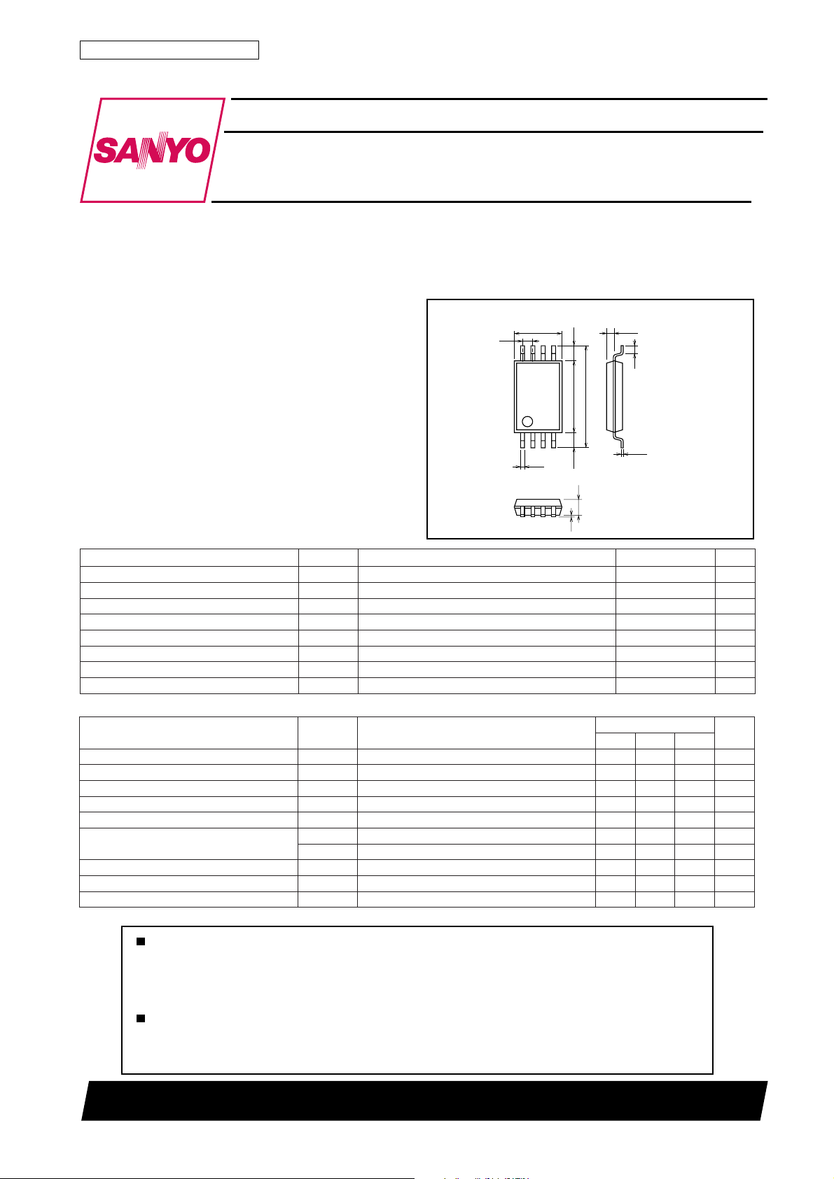
Package Dimensions
unit:mm
2155A
[FTD2017]
1 : Drain1
2 : Source1
3 : Source1
4 : Gate1
5 : Gate2
6 : Source2
7 : Source2
8 : Drain2
SANYO : TSSOP8
02V
01±V
5A
sgnitaR
8.0W
3.1W
˚C
˚C
tinU
2
×0.8mm)
nimpytxam
V,Am1=
0=02V
SG
V,V02=
0=1Aµ
SG
V,V8±=
0=01±Aµ
SD
Am1=4.03.1V
D
A5=2.1161S
D
V4=7132mΩ
SG
V5.2=0292mΩ
SG
zHM1=f,V01=0051Fp
zHM1=f,V01=053Fp
zHM1=f,V01=032Fp
21400TS (KOTO) TA-2502 No.6361–1/4
FTD2017
Continued from preceding page.
retemaraPlobmySsnoitidnoC
emiTyaleDNO-nruTt
emiTesiRt
emiTyaleDFFO-nruTt
emiTllaFt
egrahCetaGlatoTgQ
egrahCecruoS-ot-etaGsgQ 4Cn
egrahC"relliM"niarD-ot-etaGdgQ 8Cn
egatloVdrawroFedoiDV
Switching Time Test Circuit Electrical Connection
VDD=10V
V
IN
4V
0V
PW=10µs
D.C.≤1%
V
IN
G
ID=5A
RL=2Ω
D
V
OUT
)no(tiucriCtseTdeificepSeeS91sn
d
r
)ffo(tiucriCtseTdeificepSeeS09sn
d
f
V
I
DS
S
V,V01=
SD
SG
V,A5=
0=8.02.1V
SG
tiucriCtseTdeificepSeeS091sn
tiucriCtseTdeificepSeeS061sn
I,V01=
A5=
D
D2 S2 S2 G2
sgnitaR
nimpytxam
24Cn
tinU
P.G
10
3.5V
9
8
4.0V
7
–A
D
6
5
4
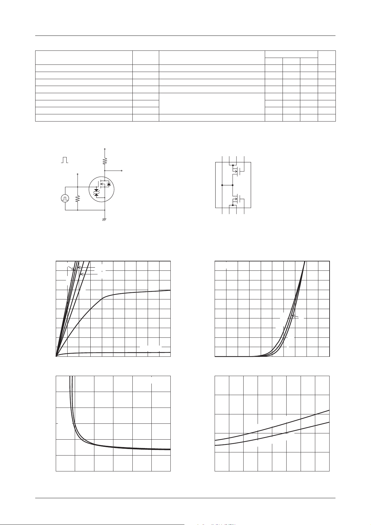
3
Drain Current, I
2
1
0
0
60
50Ω
I
D
S
-- V
FTD2017
DS
3.0V
2.5V
2.0V
VGS=1.0V
0.2
0.4 0.6 0.8 1.00.1 0.3 0.5 0.7 0.9
Drain-to-Source Voltage, VDS –V
RDS(on) -- V
GS
1.5V
IT00922
Ta=25°C
D1 S1 S1 G1
I
-- V
10
VDS=10V
9
8
7
–A
D
6
5
4
3
Drain Current, I
2
1
0
0 0.2 0.4 0.6 0.8 1.0 1.2 2.01.4 1.6 1.8
D
GS
Ta=75
°C
C
°
--25
Gate-to-Source Voltage, VGS –V
50
RDS(on) -- Ta
25°C
IT00923
50
mΩ
–
40
(on)
DS
30
ID=2A
5A
20
10
Static Drain-to-Source
On-State Resistance, R
0
0246
Gate-to-Source Voltage, VGS –V
81210
IT00924
mΩ
40
–
(on)
30
DS
20
10
Static Drain-to-Source
On-State Resistance, R
0
--25 0 25 50 75 100 125 150
- -50
=2.5V
GS
=2A, V
I
D
=4.0V
GS
=5A, V
I
D
Ambient Temperature, Ta – °C
IT00925
No.6361-2/4
 Loading...