SANYO FH102 Datasheet

FH102
Ordering number : EN5874
High-Frequency Low-Noise Amp,
Differential Amp Applications
NPN Epitaxial Planar Silicon Composite Transistor
SANYO Electric Co.,Ltd. Semiconductor Bussiness Headquarters
TOKYO OFFICE Tokyo Bldg., 1-10, 1 Chome, Ueno, Taito-ku, TOKYO, 110-8534 JAPAN
51598TS (KOTO) TA-1130 No.5874-1/5
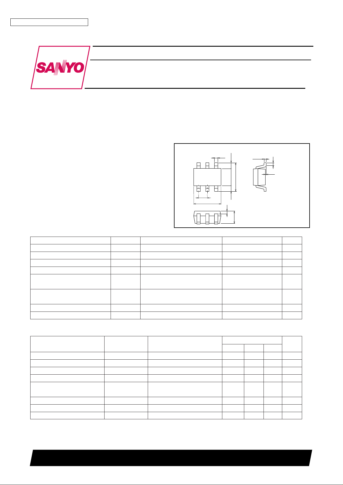
Package Dimensions
unit: mm
2149-MCP6
[FH102]
1 : Collector1
2 : Emitter1
3 : Collector2
4 : Emitter2
5 : Base2
6 : Base1
SANYO : MCP6
0‘0.1
0.65
2.0
1.25
0.4250.425
2.1
0.25
12
54
0.15
0.9
0.2
0.2
3
6
Specifications
Absolute Maximum Ratings
at Ta=25°C
Parameter Symbol Conditions Ratings Unit
Collector-to-Base Voltage V
CBO
20 V
Collector-to-Emitter Voltage V
CEO
10 V
Emitter-to-Base Voltage V
EBO
2V
Collector Current I
C
70 mA
Collector Dissipation P
C
Mounted on ceramic board 300 mW
(250mm2×0.8mm), 1unit
Total Dissipation P
T
Mounted on ceramic board 500 mW
(250mm2×0.8mm)
Junction Temperature Tj 150 °C
Storage Temperature Tstg –55 to +150 °C
Electrical Characteristics at Ta=25°C
Parameter Symbol Conditions
Ratings
min typ max
Unit
Collector Cutoff Current I
CBO
VCB=10V, IE=0 1.0 µA
Emitter Cutoff Current I
EBO
VEB=1V, IC=0 10 µA
DC Current Gain h
FE
VCE=5V, IC=20mA 90 200
DC Current Gain Ratio h
FE(small/large)VCE
=5V, IC=20mA 0.7 0.95
Base-to-Emitter Voltage V
BE(small-large)VCE
=5V, IC=20mA 1.0 mV
Difference
Gain-Bandwidth Product f
T
VCE=5V, IC=20mA 5 7 GHz
Output Capacitance Cob VCB=10V, f=1MHz 0.75 1.2 pF
Reverse Transfer Capacitance Cre VCB=10V, f=1MHz 0.5 pF
Continued on next page.
Features
• Composite type with 2 transistors contained in the MCP
package currently in use, improving the mounting
efficiency greatly.
• The FH102 is formed with two chips, being equivalent to
the 2SC5226, placed in one package.
• Optimal for differential amplification due to excellent
thermal equilibrium and pair capability.

FH102
No.5874-2/5
Continued from preceding page.
Parameter Symbol Conditions
Ratings
min typ max
Unit
Forward Transfer Gain S2le2(1) VCE=5V, IC=20mA, f=1GHz 9 12 dB
S2le2(2) VCE=5V, IC=3mA, f=1GHz 8 dB
Noise Figure NF VCE=5V, IC=7mA, f=1GHz 1.0 1.8 dB
Note) The specifications shown above are for each individual transistor except the hFE(small/large) and V
BE
(small-large) for which pair capability is also shown.
Marking : 102
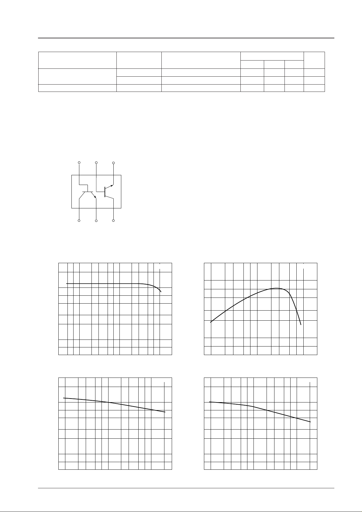
Electrical Connection
B 1 B 2 E 2
C 1 E 1 C 2
1.0
7
100
100
7
10
1.0 10 100
5
7
5
3
2
3
2
7
1.0
0.1
10
1.0
10
5
7
5
2
3
2
7
0.1
1.0
5
7
5
3
2
3
2
7
0.1
1.0
5
7
5
3
2
3
2
7
5
3 2 2
753
2
753
7532 7532 2
10
7 7532 7532 2 3
1.0
0.1
10
7 7532 7532 2 3
VCE=5V
VCE=5V
DC Current Gain, h
FE
Output Capacitance, Cob – pF
Reverse Transfer Capacitance, Cre – pF
Collector Current,I
C
– mA Collector Current,IC – mA
Collector-to-Base Voltage, V
CB
– V Collector-to-Base Voltage, VCB – V
h
FE
– I
C
f
T
– I
C
Cob – V
CB
Cre – V
CB
f=1MHzf=1MHz
Gain-Bandwidth Product,f
T
– GHz
 Loading...