

SANYO FC601 Datasheet
52098HA (KT)/41594TH (KOTO) B8-0026 No.4658-1/4
SANYO Electric Co.,Ltd. Semiconductor Bussiness Headquaters
TOKYO OFFICE Tokyo Bldg., 1-10, 1 Chome, Ueno, Taito-ku, TOKYO, 110-8534 JAPAN
TR:PNP Epitaxial Planar Silicon Transistor
SBD:Schottky Barrier Diode
DC-DC Converter Applications
Ordering number:EN4658
FC601
Specifications
Absolute Maximum Ratings at Ta = 25˚C
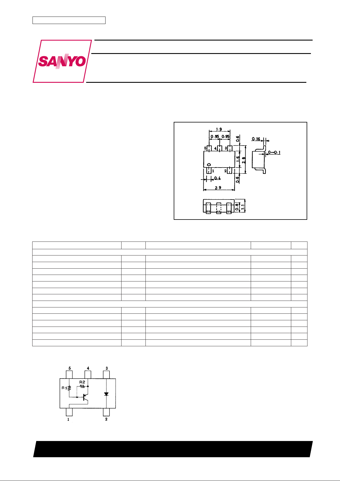
1:Collector
2:Cathode
3:Anode
4:Emitter
5:Base
SANYO:CP5
Package Dimensions
unit:mm
2105A
[FC601]
Features
· Composed of a Shottky barrier diode and a PNP
transistor with built-in resistors, and contained in one
CP package, resulting in greatly improved circuitboard using efficiency.
· The FC601 is composed of an equivalent chip to the
SB007-03CP and an equivalent chip to the RA104C
(R1=10kΩ, R2=47kΩ).
retemaraPlobmySsnoitidnoCsgnitaRtinU
]RT[
egatloVesaB-ot-rotcelloCV
OBC
05–V
egatloVrettimE-ot-rotcelloCV
OEC
05–V
egatloVesaB-ot-rettimEV
OBE
6–V
tnerruCrotcelloCI
C
001–Am
noitapissiDrotcelloCP
C
002Wm
erutarepmeTnoitcnuJjT 051
erutarepmeTegarotSgtsT 051+ot55–
]DBS[
egatloVesreveRkaePevititepeRV
MRR
03V
egatloVegruSesreveRkaePevititeper-noNV
MSR
53V
tnerruCtuptuOegarevAI
O
07Am
tnerruCdrawroFegruSI
MSF
elcyc1,evaweniszH05 2A
erutarepmeTnoitcnuJjT 521+ot55–
erutarepmeTegarotSgtsT 521+ot55–
Marking:601
Electrical Connection
1:Collector
2:Cathode
3:Anode
4:Emitter
5:Base
˚C
˚C
˚C
˚C
Continued on next page.
FC601
No.4658-2/4
Continued from preceding page.
Electrical Characteristics at Ta=25˚C
˚C/W
retemaraPlobmySsnotidnoC
sgnitaR
tinU
nimpytxam
]RT[
tnerruCffotuCrotcelloCI
OBC
V
BC
I,V04–=
E
0=1.0–Aµ
tnerruCffotuCrotcelloCI
OEC
V
EC
I,V04–=
B
0=5.0–Aµ
tnerruCffotuCrettimEI
OBE
V
BE
I,V5–=
C
0=76–88–521–Aµ
niaGtnerruCCDh
EF
V
EC
I,V5–=
C
Am5–=07
tcudorPhtdiwdnaB-niaGf
T
V
EC
I,V01–=
C
Am5–=002zHM
ecnaticapaCtuptuOboCV
BC
zHM1=f,V01–=3.5Fp
egatloVnoitarutaSE-CV
)tas(EC
I
C
I,Am01–=
B
Am5.0–=1.0–3.0–V
egatloVnwodkaerBB-CV
OBC)RB(
I
C
I,Aµ01–=
E
0=05–V
egatloVnwodkaerBE-CV
OEC)RB(
I
C
R,Aµ001–=
EB
=∞ 05–V
egatloVetatS-FFOtupnIV
)ffo(I
V
EC
I,V5–=
C
Aµ001–=6.0–8.0–0.1–V
egatloVetatS-NOtupnIV
)no(I
V
EC
I,V2.0–=
C
Am5–=7.0–0.1–0.2–V
ecnatsiseRtupnI1R70131kΩ
oitaRecnatsiseR2R/1R 312.0
]DBS[
egatloVesreveRV
R
I
R
Aµ02=03V
egatloVdrawroFV
F
I
F
Am07= 55.0V
tnerruCesreveRI
R
VRV51= 5Aµ
ecnaticapaClanimretretnICV
R
zHM1=f,V01=0.3Fp
emiTyrevoceResreveRt
rr
IFI=
R
tiucriCtseTdeificepseeS,Am01= 01sn
ecnatsiseRlamrehTa-jhtR 026
T rr Test Circuit
 Loading...