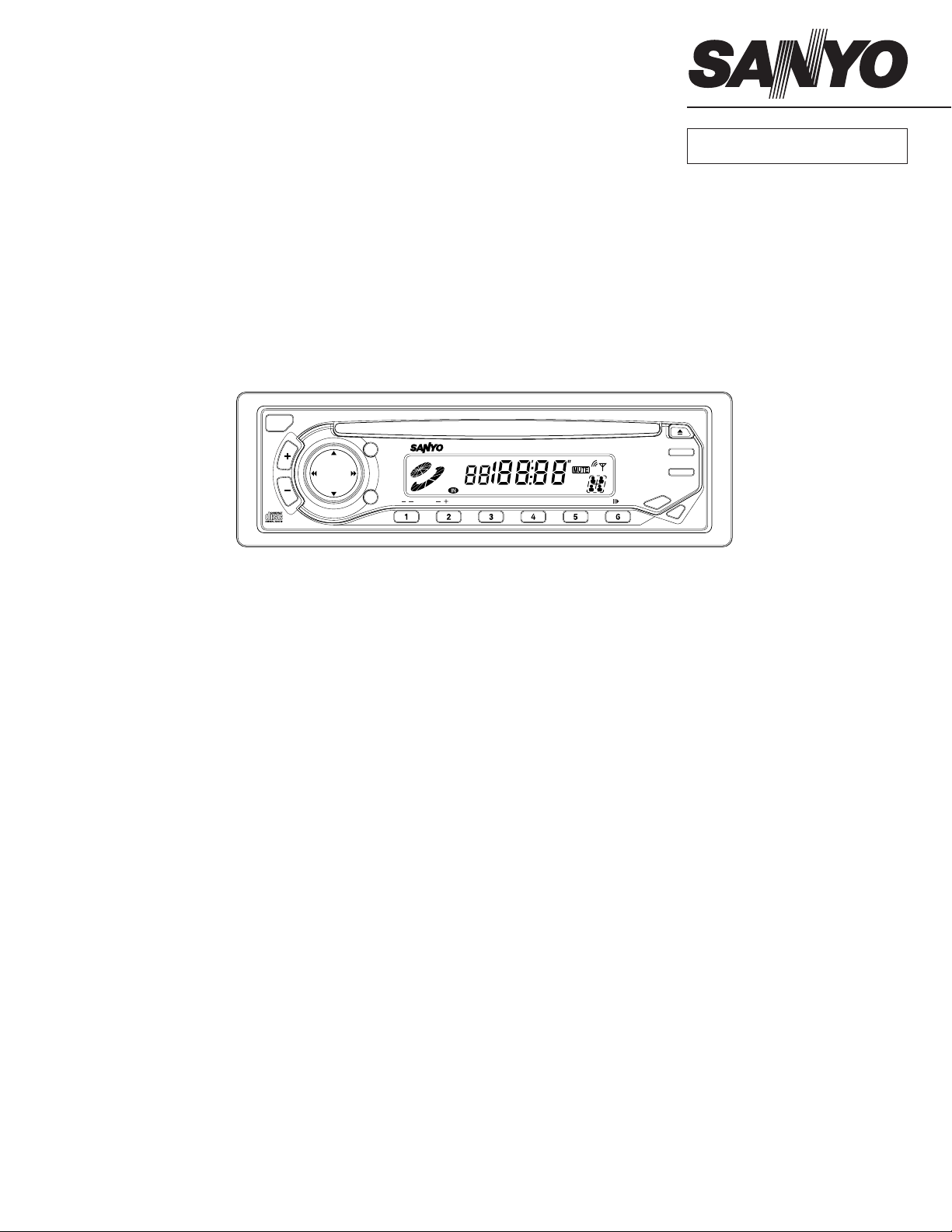
Sanyo ECD-780 Service manual
FILE NO.
SERVICE MANUAL
REL
VOL
TUN
TRK
Specifications
FM TUNER
Tuning Range.............................................................................. 87.5 - 107.9 MHz. (200 KHz. step)
Sensitivity .................................................................................... 1.5 µV
Separation................................................................................... 30 dB
Signal-to-Noise Ratio .................................................................. 65 dB (stereo), 70 dB (mono)
Full Panel Detachable
High Power
FM / AM Stereo Receiver
Compact Disc Player
LO/DX
LOUD
AUD
FM/AM CD RECEIVER ECD-780 45W x 4
PRESET
TRACK
CD
FMIII
AMII
LOUD ST LOC
L
R
BASS MANU TRE
R
F
SCAN
SHF
RPT
RPTSHFDISC
ECD-780
114782838
BAND
ATP
FRONT
CDC
CD
DISP
PWR
MUTE
AM TUNER
Tuning Range.............................................................................. 530 - 1,710 KHz. (10 KHz. step)
Sensitivity .................................................................................... 20 µV
Signal-to-Noise Ratio .................................................................. 45 dB
CD PLAYER
Frequency Response .................................................................. 20 - 20,000 Hz.
Signal-to-Noise Ratio .................................................................. 90 dB
Channel Separation .................................................................... 60 dB
Dynamic Range .......................................................................... 90 dB
Harmonic Distortion..................................................................... 0.2 %
AUDIO AMPLIFIER & GENERAL
Maximum Output Power ............................................................. 45 W x 4 channels
Output Wiring .............................................................................. Floating-Ground type designed for
4-speaker use
RCA low-level outputs: 2 channels
Output Impedance ...................................................................... 4 - 8 ohms
Power Supply .............................................................................. 12 volts DC, negative ground
Specifications are subject to change without notice.
REFERENCE No. SM-7900004

CONTENTS
SERVICE NOTES and PRECAUTIONS.........................................................................2-4
ELECTRICAL ADJUSTMENTS.......................................................................................5-8
TERMINOLOGY REFERENCE ....................................................................................9-13
BLOCK DIAGRAM ........................................................................................................... 14
IC/TRANSISTOR LEAD IDENTIFICATION...................................................................... 15
CD MECHANISM EXPLODED VIEW .............................................................................. 16
PARTS LIST - CD MECHANISM.................................................................................17-18
CABINET & CHASSIS EXPLODED VIEW....................................................................... 19
PARTS LIST - CABINET, CHASSIS AND ACCESSORIES.............................................. 20
PARTS LIST-MAIN ......................................................................................................21-25
PARTS LIST-DISP ......................................................................................................26-27
PARTS LIST-RF33 ......................................................................................................28-30
CIRCUIT BOARD DIAGRAM ............................................................... SEPARATE SHEET
SCHEMATIC DIAGRAM ...................................................................... SEPARATE SHEET
— 1 —

SERVICE NOTES AND PRECAUTIONS
SERVICE NOTES
1. Make sure that the power lead is connected properly to
power source, otherwise damage to radio may result. If a
battery eliminator is used as a power source in place of a
battery, it must be filtered and regulated. (The power supply capacity should be more than 5 amps.)
2. Integrated circuits (ICs) are used in this unit. Because the
ICs are direc-coupled devices, as to all electronic equipment, reading within 10% of the indicated values are acceptable. Allowance must also be made for variations in
supply voltage. It is expected that any breakdown within
the IC results in drastic changes of the operating voltages
at the terminals.
3. When replacing a power output IC, remember to use the
IC specified in the parts list; Coat the IC-fin with silicon
grease.
WARNING
ln using meters, signal generator and any tool in servicing
Ics, extreme care is needed. DO NOT SHORT THE IC TERMINALS TO THE PATTERN ON THE PC BOARD OR TO
EACH OTHER. THE IC WILL BE INSTANTANEOUSLY DESTROYED.
ALIGNMENT PROCEDURE
Alignment is performed at factory with laboratory equipment.
Therefore, before alignment is attempted, the unit should be
thoroughly checked for circuit troubles.
NOTES:
1. Check for specified source voltage-DC, 14.4volts.
2. Connect an AC voltmeter (AC VM) across speaker or
dummy load (4 ohms. 20W , wirewound resistor)...see Fig.
1-3. (ELECTRICAL ADJUSTMENTS)
3. Signal input must be kept as low as possible to avoid overload and clipping (use highest sensitivity of output indicator).
4. Repeat adjustment to ensure good results.
5. Non-metallic alignment tools must be used (especially at
FM alignment).
6. For alignment location details, refer to CIRCUIT BOARD
PARTS LOCATION.
INSTALLATION PROCEDURE
1. To prevent a short circuit, remove the key from the ignition and disconnect the
2. Make the proper input and output wire connections for
each unit.
3. Connect the wiring harness wires in the following order:
ground, speakers, battery, ignition.
4. Connect the wiring harness connector to the unit.
5. Install the unit in your car.
6. Reconnect the
7. Disinstall by reversing the installation procedure.
battery.
battery.
CAUTI0N
• The rear-panel which also heatsink is very hot. Don’t burn!!
• If your car’s ignition does not have an ACC position, connect the ignition wires to a power source that can be turned
on and off with the ignition key . If you connect the ignition
wire to a power source with a constant voltage supply, as
with battery wires, the battery may die.
• If the console has a lid, make sure to install the unit so
that the cover will not hit the lid when closing and opening.
• If the fuse blows, first make sure the wires aren’t touching
to cause a short circuit, then replace the old fuse with one
with the same rating.
• Do not let unconnected wires or terminals touch metal on
the car or anything else conducting electricity. To prevent
a short circuit, do not remove the caps on the ends of the
unconnected wires or the terminals.
• Connect the speaker wires correctly to the terminals to
which they correspond. The unit may be damaged or fail
to work if you share the
metal part in the car.
• After the unit is installed, check whether the brake lamps,
blinkers, wipers, etc. on the car are working properly.
• Insulate unconnected wires with vinyl tape or other similar material .
wires or ground them to any
— 2 —
SERVICE NOTES AND PRECAUTIONS
LASER BEAM SAFETY PRECAUTIONS
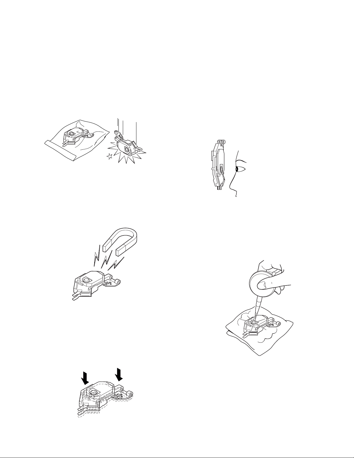
NOTES FOR TRANSPORT AND STORAGE
1. The pickup should always be kept in its conductive bag
until use.
2. The pickup should never be subjected to external pressure or impact.
Storage in conductive bag Drop impact
GOOD
REPAIR NOTES
1. The pickup incorporates a strong magnet, and so should
never be brought close to magnetic materials.
NG
3. Each and every pickup is already individually adjusted to
a high degree of precision, and for that reason the adjustment point and installation screws should be absolutely
never be touched.
4. Laser beam may damage the eyes!
Absolutely never permit laser beams to enter the eyes!
Also NEVER switch ON the power to the laser output part
(lens, etc.) of the pickup if it is damaged.
Laser Beam
NEVER look directly at the
laser, and do not let contact
fingers of other exposed
skin.
NG
Magnet
NG
2. The pickup should always be handled correctly and carefully, taking care to avoid external pressure and impact. If
it is subjected to strong pressure or impact, the result may
be an operational malfunction and/or damage to the
printed circuit board.
Pressure
Pressure
5. Cleaning the lens surface
If there is dust on the lens surface, the dust should be
cleaned away by using an air brush (such as one used for
camera lens). The lens is held by a delicate spring.
Conductive Sheet
6. Never attempt to disassemble the pickup.
— 3 —
SERVICE NOTE AND PRECAUTIONS
STATIC ELECTRICITY
The CD pickup might suffer destruction by static electricity during spare-parts maintenance or replacement, although it is stable
when connected to the circuit in the CD unit. The destruction might be caused because the laser diode terminal will be electrically open. To prevent the terminal from being open, do the following steps:
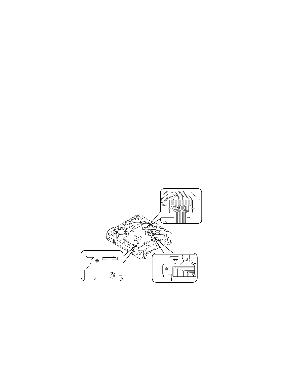
1. When you replace the CD pickup, or remove the CD unit from the car stereo unit for any maintenance purpose, solder the
copper foil pattern indicated in Fig. 1 and Fig. 2 below to short-circuit the connector PCB and flexible wire of the CD unit.
Perform your intended maintenance work with the flexible wire short-circuited.
2. If the original CD pickup may possibly be reused, make a short circuit in the area indicated in Fig. 3 first. Then remove the
pickup and perform the work.
3. The CD Pickup OPTIMA-715K2, which is supplied as one of the spare parts, is already short-circuited with the copper foil
pattern pre-soldered indicated in Fig. 3 below. To handle this CD Pickup, keep the short circuit as it is. Then attach the
Pickup to the unit and connect the flexible wire to the connector.
4. After performing the work, eliminate the short circuit by removing the solder at its respective short-circuited area described
in 1, 2 and 3 above.
5. Insert a CD. If the E-01 or E-02 error should appear on the display on the face plate, check the area mentioned in 4 above,
where the short circuit may not have been eliminated.
6. Note that the semi-fixed VR equipped with the CD Pickup OPTIMA-715K2 must not be turned. You cannot make any
adjustment to the semi-fixed VR, which is completely adjusted when shipped at the factory.
Fig. 3Fig. 2
Fig. 1
— 4 —
DUMMY BOX SCHEMATIC
ELECTRICAL ADJUSTMENTS
AM S.G.
(50Ω)
CO-AX CABLE
33Ω 15PF
60PF
PLUG TO FIT ANTENNA
RECEPTACLE OF UNIT
METAL SHIELD CAN
FM S.G.
(50Ω)
CO-AX CABLE
10Ω 45Ω
60Ω
PLUG TO FIT ANTENNA
RECEPTACLE OF UNIT
METAL SHIELD CAN
AM DUMMY ANTENNA FM DUMMY ANTENNA
Fig. 1-1 Fig. 1-2
4Ω 20W
LEFT CHANNEL OUTPUT
UNIT
RIGHT CHANNEL OUTPUT
4Ω 20W
L
R
L
R
AC V.T.V.M. OR SCOPE
DUMMY LOAD & SWITCH BOX (FOR STEREO UNIT)
Fig. 1-3
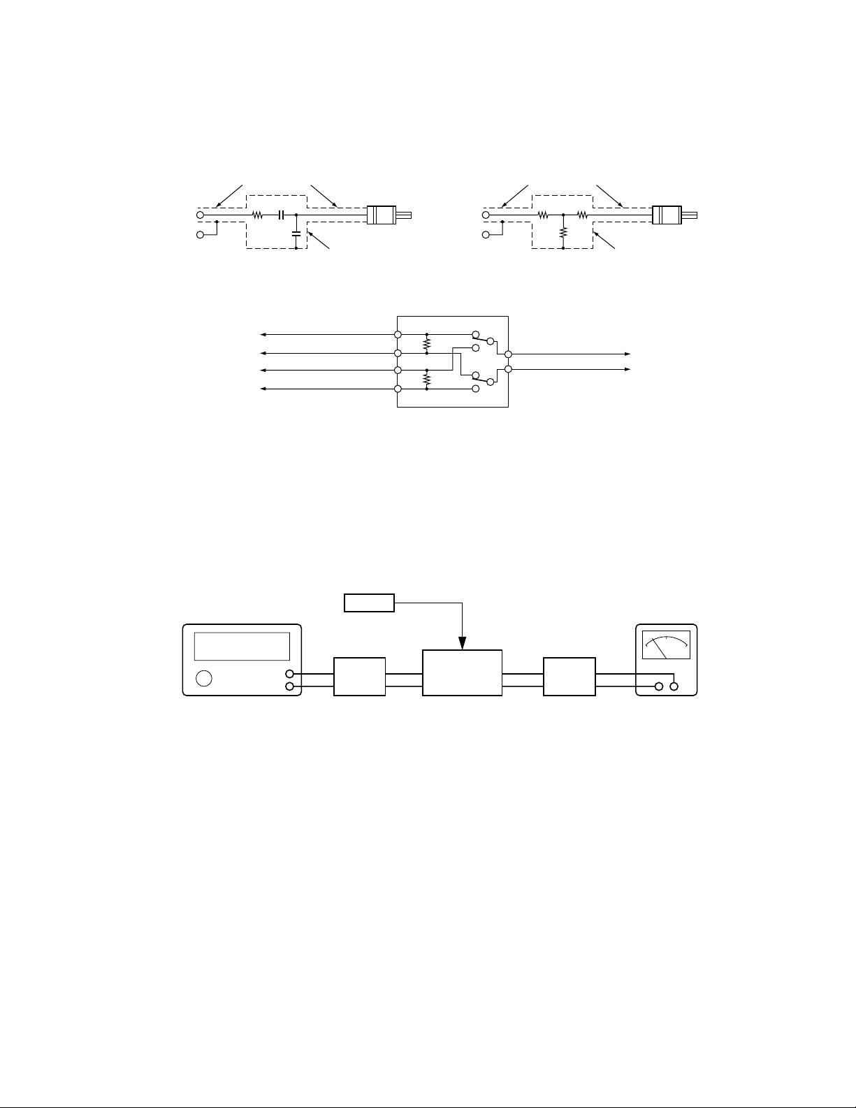
ALIGNMENT OF AM RF & lF SECTI0N
Set the radio for AM reception. AM signal generator should be coupled with antenna receptacle through dummy (see Fig.1-1).
Set VOLUME control to maximum and TONE to center. Attenuate signal generator output to maintain 0.5 watts (1.4 volts across
4 ohms load) on AC voltmeter.
FM SG
&
STEREO SG
VTVM
(See Fig. 1.2)
FM
DUMMY
ANTENNA
DISTORTION METER
AC VOLTMETER
T.P
SET
(See Fig. 1.3)
DUMMY
LOAD &
SW BOX
Fig. 2 * SG frequency should be as accurate as possible.
— 5 —
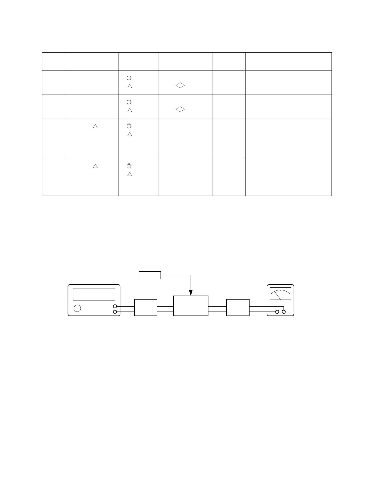
ELECTRICAL ADJUSTMENTS
STEP
1
2
3
GENERATOR
FREQUENCY
Non-Mod.
Non-Mod.
1000kHz, 999kHz
400Hz
30% MOD
RADIO DIAL
SETTING
530kHz
531kHz
1710kHz
1602kHz
1000kHz
999kHz
OUTPUT
INDICATOR
DC VTVM to test
point
DC VTVM to test
point
AC VTVM across
speaker(L or R) or 4
ohms load
SG att: 20dBµ
4
1000kHz, 999kHz
400Hz
30% MOD
1000kHz
999kHz
TEST MODE
Adjust so that the
“ST” mark of LCD
Display appears
SG att: 30dBµ
SETTING UP TEST MODE AT STEP 4 - SEE PAGE 8
ADJUST-
MENT
—
VT
—
VT
L108
Check the voltage more than
2.2V
Check the voltage less than 7.5V.
Adjust for Maximum Level.
REMARKS
AM IFT1
L111
AM IFT2
R124
AM SD
Sensitivity of the seeking frequency.
ALIGNMENT OF FM RF & IF SECTION
Set the radio for FM reception. FM signal generator should be coupled with antenna receptacle, through dummy (see Fig.1-2).
FM SG
&
STEREO SG
VTVM
(See Fig. 1.2)
FM
DUMMY
ANTENNA
T.P
SET
(See Fig. 1.3)
DUMMY
LOAD &
SW BOX
DISTORTION METER
AC VOLTMETER
Fig. 3 * SG frequency should be as accurate as possible.
— 6 —
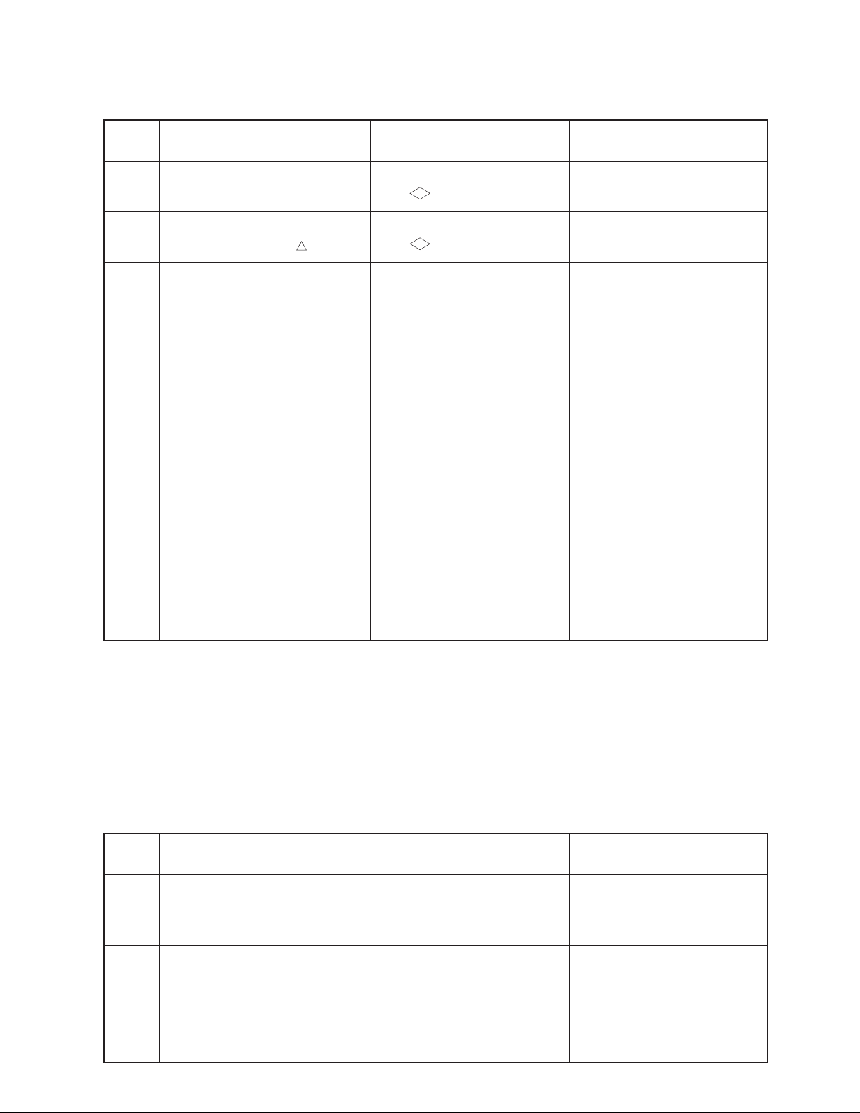
ELECTRICAL ADJUSTMENTS
STEP
1
2
3
4
5
6
GENERATOR
FREQUENCY
Non-Mod.
Non-Mod.
98.1MHz
1kHz, 22.5kHz dev .
SG att:66dBµ(1mV)
98.1MHz
1kHz, 22.5kHz dev .
SG att:6dBµ
98.1MHz
SG att:6dBµ
88.5MHz
107.1MHz
SG att:6dBµ
RADIO DIAL
SETTING
87.5MHz
107.9MHz
108MHz
98.1MHz
98.1MHz
98.1MHz
88.5MHz
107.1MHz
OUTPUT
INDICATOR
DC VTVM to test
VT
point
DC VTVM to test
VT
point
AC VTVM to test
point*
AC VTVM across
speaker or 4 ohms
load
AC VTVM across
speaker or 4 ohms
load
AC VTVM across
speaker or 4 ohms
load
ADJUST-
MENT
—
L103
FM OSC
L110
FM DET
L107
FM MIX
L100
FM ANT
L102
FM RF
L100
FM ANT
L102
FM RF
REMARKS
Check the voltage more than 1.1V
Adjust for 6.9 앐0.1V
NULL VOLTAGE to become -20
앐20mV
Adjust for Maximum Level.
Adjust for Maximum LeveL.
Check for SPEC.
7
98.1MHz
SG att:25dBµ
98.1MHz
TEST MODE
Adjust so that the
“ST” mark of LCD
Display appears
SETTING UP TEST MODE AT STEP 7 - SEE PAGE 8
ALIGNMENT OF FM MULTIPLEX SECTION
FM signal generator should be modulated by FM stereo signal generator.
Modulation level: 19kHz 10% (7.5kHz dev)
1000Hz 30% (22.5kHz dev)
FM signal generator output level: 66dBµ (1mV)
Frequency: 98.1 MHz.
STEP
1
2
MODULATION
FREQUENCY
19kHz & 1000Hz
(Left Channel)
SG att:66dBµ
19kHz & 1000Hz
(Right Channel)
OUTPUT INDICATOR
AC VTVM across Right speaker or
Right channel load
AC VTVM through Left speaker or
Left channel load
R129
FM SD
Set the radio for FM reception and tune to signal. Adjust volume control to provide 0.5 watt on AC VTVM and tone to
center. Set L/R balance control for equal output at each channel.
ADJUST-
MENT
R137
R137
Sensitivity of the seeking frequency.
REMARKS
Adjust for minimum.
Check for minimum.
3
19kHz & 1000Hz
(Left Channel)
SG att:47dBµ
AC VTVM across Right speaker or
Right channel load
— 7 —
R156
Adjust for 20dB Separation.
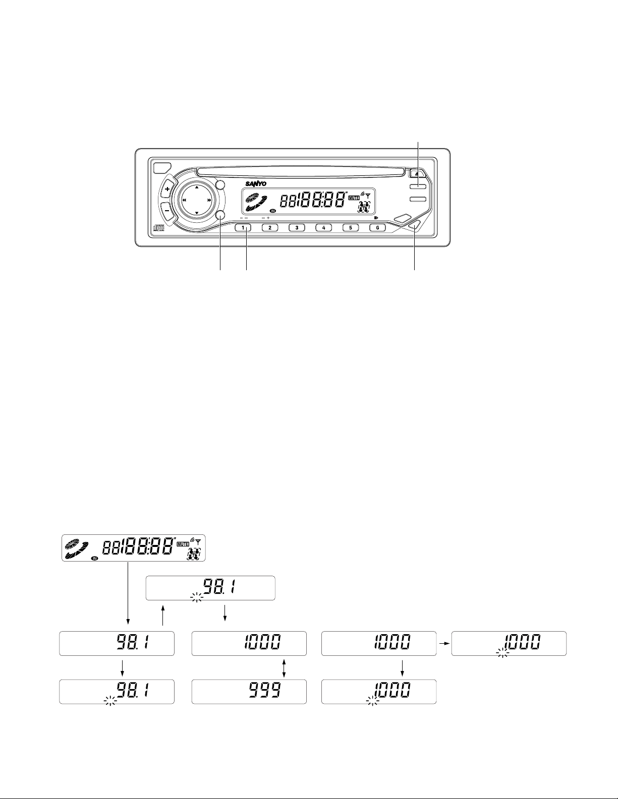
ELECTRICAL ADJUSTMENTS
SETTING UP TEST MODE AT STEP 4 FOR AM & STEP 7 FOR FM
Press the e
the mode to the test mode shown in Step 4 for AM and Step 7 for FM.
PWR
button to turn the power off. Next, use the following procedure with the front panel switches to set
w
REL
VOL
TUN
TRK
LO/DX
LOUD
AUD
FM/AM CD RECEIVER ECD-780 45W x 4
PRESET
TRACK
CD
FMIII
AMII
LOUD ST LOC
L
R
BASS MANU TRE
R
F
SCAN
SHF
RPT
RPTSHFDISC
FRONT
BAND
ATP
CD
CDC
DISP
PWR
MUTE
er q
Fig. 4
1. While the power is off, press the q
to enable the w
BAND
button to be used at the moment the power comes on.
PRESET 1
button. Then press the w
BAND
button and e
PWR
button simultaneously
2. If the above operation is successful all the figures on the LCD light up, check that you have entered test mode. Fig. 5(A).
3. Press the r
AUD
button once. The display shown in Fig. 5(B) appears on the LCD and the unit enters DX mode.
Then, while receiving FM 98.1MHz rotate the Semi-fixed VR R129 on the TUNER UNIT (RF33) to adjust the LCD until the
stereo mark light “ST” is on. Fig. 5(B)’.
4. Press the r
AUD
button, if the display changes to that shown in Fig. 5(C) the unit is in Local mode. Check that the “ST” mark
is displayed (for specific: Input level is 12 ~ 28dB higher than that of the DX mode).
5. Press the w
6. Then press the r
BAND
button, if the display changes to that shown in Fig. 5(D) or (D)’ receiving AM 1000 kHz or *(999) kHz.
AUD
button, if the display changes to that shown in Fig. 5(E) the unit is in DX mode. Rotate the Semi-fixed
VR R124 on the TUNER UNIT (RF33) to adjust the LCD until “ST” mark lights up.
7. Then press the r
AUD
button, if the display changes to that shown in Fig. 5(F) the unit is in Local mode. Check that the “ST”
mark is displayed. (for specific: Input level is 12 ~ 28dB higher than that of DX mode).
8. Turn off the power to release the test mode.
TEST MODE CHART
(A) Enter the Test Mode
PRESET
CD
FMIII
AMII
LOUD ST LOC
TRACK
L
R
R
F
SCAN
SHF
BASS MANU TRE
RPT
(C) FM Local Mode OK
FMI
FRONT
ST LOC
(B) FM DX Mode
FMI
(B’) CK
FMI
ST
(D) Receiving 1000kHz
AMI
(D’) Receiving 999kHz
AMI
(E) AM DX Mode
(F) AM Local Mode
Fig. 5
— 8 —
AMI
AMI
ST LOC
(E’) OK
AMI
ST
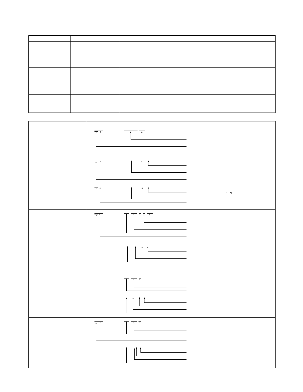
TERMINOLOGY REFERENCE
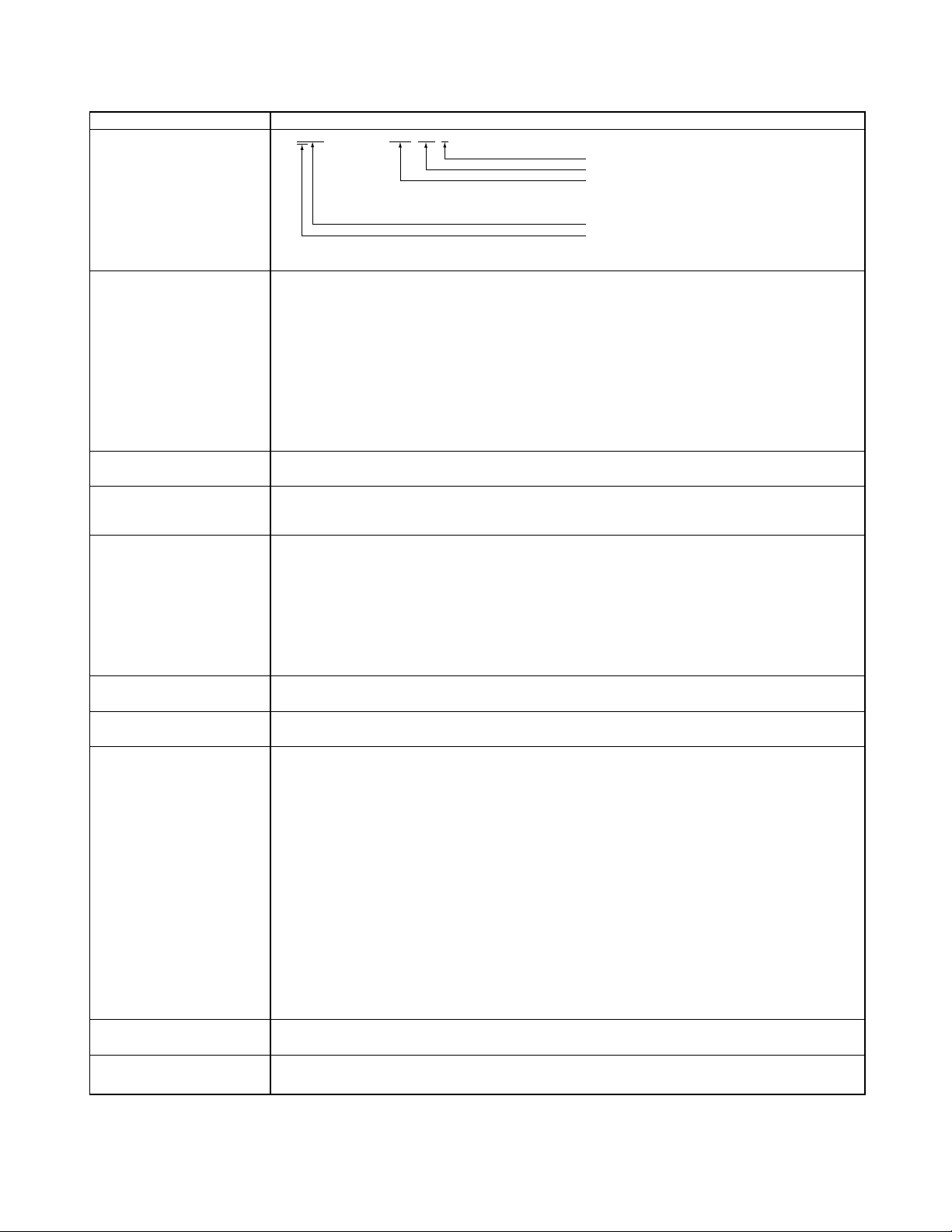
Parts Name CAD-Code Numerical Value
Chip Capacitor CAR75C R75=0.75pF
Chip Tantalum CAT0.1/35E 0.1/35=0.1µF / 35V
Electrolytic Capacitor ES47/16 47/16=47µF / 16V
Chip Resistor RBR68 R68=0.68 Ω
Coil LAUR22T R22=0.22 µH
The following terms have been changed as a result of the use of a new CAD system.
Parts Name
IC IC101 LA3373. MT
Hybrid IC IC102 HIC . . . . . . Code No. (3-8 Column 씮 11. . . . . .0)
Transistor Q101 2SC2785 T. E.F
Diode D101 MTZJ3.0. A. RT
Chip Capacitor C101 CA 102 S J 100
Chip Tantalum C102 CAT 0.1 /35 E
Chip Trimmer C103 CT. . . . . . Code No. (3-8 Column 씮 15. . . . . .0)
Trimmer Capacitor C104 CT. . . . . . Code No. (3-8 Column 씮 15. . . . . .0)
Ceramic Capacitor C105 CH 102 H
Electrolytic Capacitor C106 ES 47/ 16 H
Chip Resistor R101 RA 202 G
Resistor R102 RC 1R0 R
CA3R0C 3R0=3.0pF
CA100U 100=10 x 10
CA333B 333=33 x 10
CA104F 104=10 x 10
RA1R0 1R0=1.0 Ω
RA180 180=18 x 10
RA821 821=82 x 10
RA102 102=10 x 10
LAY2R2T 2R2=2.2 µH
LAY330T 330=33 x 10
LAY151T 151=15 x 10
Circuit Ref. No. CAD Code Description
0
=10pF
3
=33000pF=0.033µF
4
=0.1 x 10⁶pF=0.1µF
0
=18 Ω
1
=820 Ω
2
=1000 Ω=1KΩ
0
=33 µH
1
=150 µH
Taping or Forming Type
Description (LA3373)
Circuit Ref. Number
Head Name
hfe Rank
Taping Type
Description (2SC2785)
Circuit Ref. Number
Head Name
Taping or Forming Type
Rank
Description (MTZJ3.0)
Circuit Ref. Number
Head Name
Voltage Proof
Tolerance
Temperature Characteristic
Capacitance (10 x 102=0.1 x 10⁴pF=0.001µF)
Chip Capacitor Type
Circuit Ref. Number
Head Name
Maker Mark
Voltage Proof (35V)
Capacitance (0.1µF)
Chip Tantalum Capacitor Type
Taping or Forming Type
Capacitance (12 x 10
Temperature Characteristic
Taping or Forming Type
Voltage Proof (16V)
Capacitance (47µF)
Electrolytic Capacitor Type
Resistance Tolerance
Resistance (20 x 102=2KΩ)
Chip Resistor Type
Circuit Ref. Number
Head Name
Taping or Forming Type
Resistance (1.0Ω)
R : Decimal Point Mark
Resistor Type
0
=12pF)
— 9 —
TERMINOLOGY REFERENCE
Parts Name Circuit Ref. No. CAD Code Description
Coil L101 LAY 151 T
Taping or Forming Type
Inductance (15 x 10
Coil Type
L : Fixed Letter
A : Maker Mark
Y : Part Forming (or Size)
Circuit Ref. Number
Head Name
Transformer L101 L . . . . . . Code No. (3-8 Column 씮 17. . . . . .0)
Antenna ANT101 ANT. . . . . . Code No. (3-8 Column 씮 10. . . . . .0)
Battery BT101 BT. . . . . .
Buzzer BUZ101 BUZ. . . . . .
Dew Sensor PQ101 Code No. Code No. 1000. . . . . .
Electric Tuner ET101 ET. . . . . .
Relay K101 K. . . . . .
Emblem SW Assy MB101 MB. . . . . .
Microphone MC101 MC. . . . . .
Module MD101 MD. . . . . .
Motor Stator Assy MS101 MS. . . . . .
Manual Tuner MT101 MT. . . . . .
Push Button Tuner PT101 PT. . . . . .
Switch Power Unit PW101 PW. . . . . .
CR Component CR101 CR. . . . . . Code No. (3-8 Column 씮 11. . . . . .0)
IN-line Block IB101 IB. . . . . .
Surge Absorber Z101 Z. . . . . . Code No. (3-8 Column 씮 13. . . . . .0)
Ceramic Varistor Z102 Z. . . . . .
Silicon Varistor Z103 Z. . . . . .
FIP H101 FIP. . . . . . Code No. (3-8 Column 씮 14. . . . . .0)
LCD H102 LCD. . . . . .
LED LD101 LED. . . . . .
Neon Bulb NE101 NE. . . . . .
Photo Diode PD101 PD. . . . . .
Photo Coupler PH101 PH. . . . . .
Photo Interruptor PI101 PI. . . . . .
Pilot Lamp PL101 PL. . . . . .
Photo Transistor PQ101 PQ. . . . . .
CCD Y101 Y. . . . . .
Ceramic Filter F101 F. . . . . . Code No. (3-8 Column 씮 17. . . . . .0)
Crystal F102 F. . . . . .
Printeed Circuit Board W101 Code No. Code No. 18. . . . . .
Block PC Assy BL101
Wire N101 Code No. Code No. 191. . . . . .
QS-CONN N102
Shield Wire N103
Flat Wire N104
Coaxial N105
Strip Wire N106
Flat Wire N107
Flexible Wire N108
Strip Wire N109
QS-CONN N110
" N111
" N112
" N113
Antenna Jack AJ101
QS-CONN N101
POST P101
Jumper J101
RT Pin TP101
Check Pin TP102
IC Socket P102
Switch SW101 Code No. 23. . . . .
Volume Rv101
Fuse Z101
Fuse Holder FH101
"
"
"
"
"
"
"
"
"
"
"
"
"
"
"
"
"
"
"
"
"
"
"
"
"
"
"
"
"
"
"
"
"
"
"
"
"
"
"
"
"
"
"
"
"
"
"
"
"
Code No. 192. . . . . .
"
"
Code No. 193. . . . . .
Code No. 194. . . . . .
"
Code No. 195. . . . . .
Code No. 1960. . . . .
Code No. 1961. . . . .
Code No. 1962. . . . .
Code No. 1963. . . . .
Code No. 1965. . . . .
Code No. 196A. . . . .
Code No. 1981. . . . .
Code No. 1983. . . . .
Code No. 1984. . . . .
"
Code No. 1985. . . . .
"
"
"
1
=150µH)
— 10 —
TERMINOLOGY REFERENCE
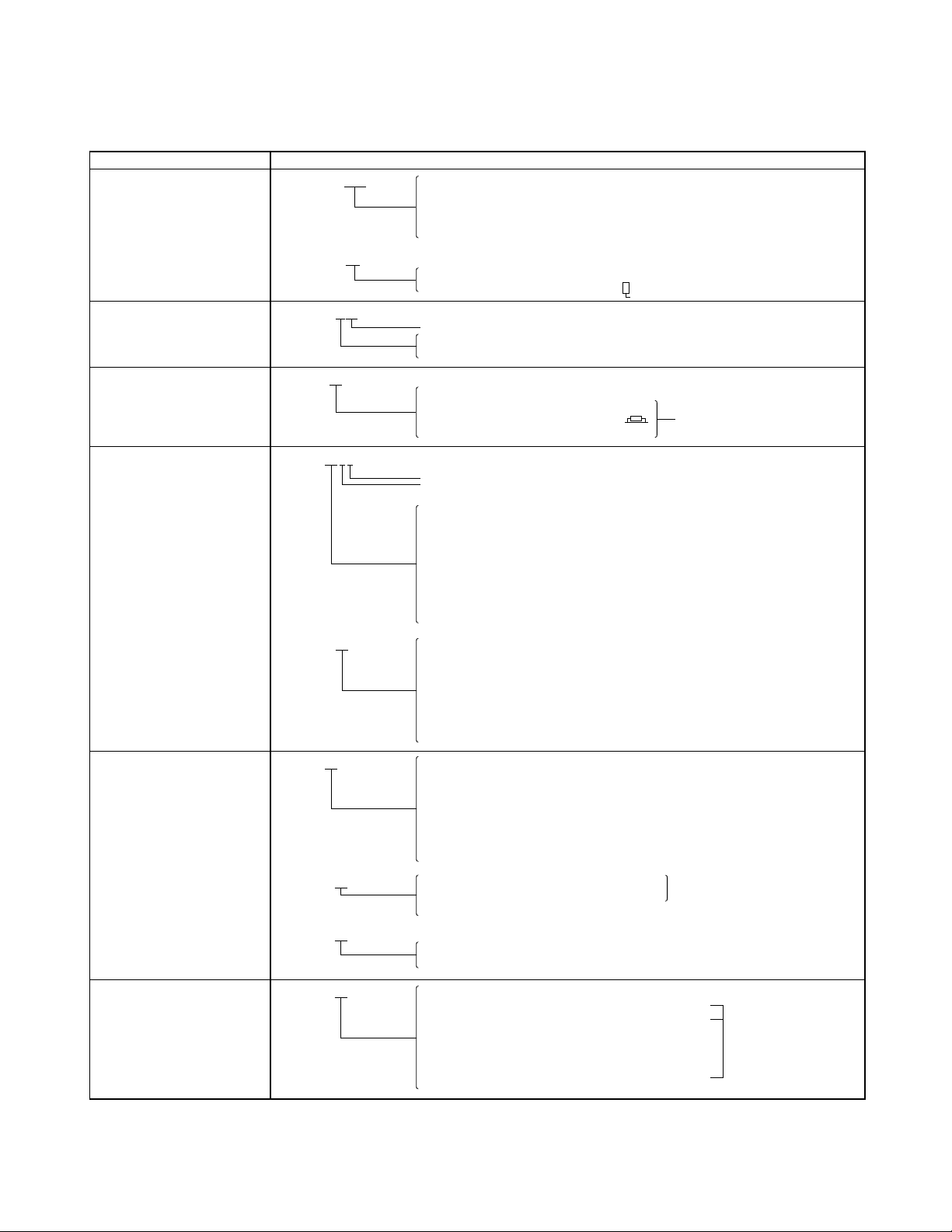
Details of CAD Code
Parts Name CAD Code Mark Name Taping or Forming Type
IC UPC4570C. ** No Mark Hand Insert
MT Stick
CT Chip
MF Mini Flat
YC Tray
HIC500850 *
No Mark Straight Type
L L Type
Transistor 2SC2785*. * *Z
*.* (* and *) hfe Rank
No Mark Hand Insert
T Radial/Chip—Z : Cancel Machine Insert
Diode 1SS245 *
No Mark Hand Insert
.FT Forming Type
.RT Radial
T Axial
Chip CA100 * * *
Capacitor Voltage limit
Tolerance
Temperature Characteristic
C : CH (0앐60PPM/ ˚C) (-55~+125˚C)
: CJ (0앐120PPM/ ˚C) (-55~+125˚C)
: CK (0앐250PPM/ ˚C) (-55~+125˚C)
U : UJ (-750앐120PPM/ ˚C) (-25~+85˚C)
S : SL (+350~-1000PPM/ ˚C) (-25~+85˚C)
B: B (앐10PPM/ ˚C) (-25~+85˚C)
R : RH (-220앐60PPM/ ˚C) (-25~+85˚C)
F : F (+30 ~ -80 ~) (-25~+85˚C)
The other Capacitors ES3.3/50 * Z No Mark Radial (5mm Pitch)
F Hi—F Part
S Straight Type
L Radial (2.5mm Pitch)
H Hand Insert
SH No kink (Straight)
FSH With Kink (Short Lead/Radial type)
KSH With kink (Short Lead)
Z : Cancel Machine Insert
Chip Resistor RA100 * Tolerance
B(앐0.1%)
D(앐0.5%)
F(앐1%)
G(앐2%)
J(앐5%) : No Mark
K(앐10%)
M(앐20%)
Resistor (1/6 [W]) RC100 * Z No Mark Axial
R Radial
H Hand Insert
The other Resistors RCAR47 *
H Hand Insert
HP Press Forming (Hand Insert)
Coil LAY151 * No Mark Hand Insert
A Axial
C Chip
K With kink (Hand Insert)
L Long Lead
M Stick
R Radial
T Radial
— 11 —
Z : Cancel Machine Insert
Z : Cancel Machine Insert
 Loading...