

Page 1
FILE NO.
Service Manual
z/ON
123
TUNER
/BAND
456
PRESET
789
SLEEP
0
ADJUST
SET/CLEAR
CLOCKTIMER
TIME SET
DISC SELECT
fe
i
REPEAT
RANDOM MEMORY
n
TAPE-A/B REC MUTE
a
ncjd
SOUND
VIDEO/DVD
PRESET
MUTE
VOLUME
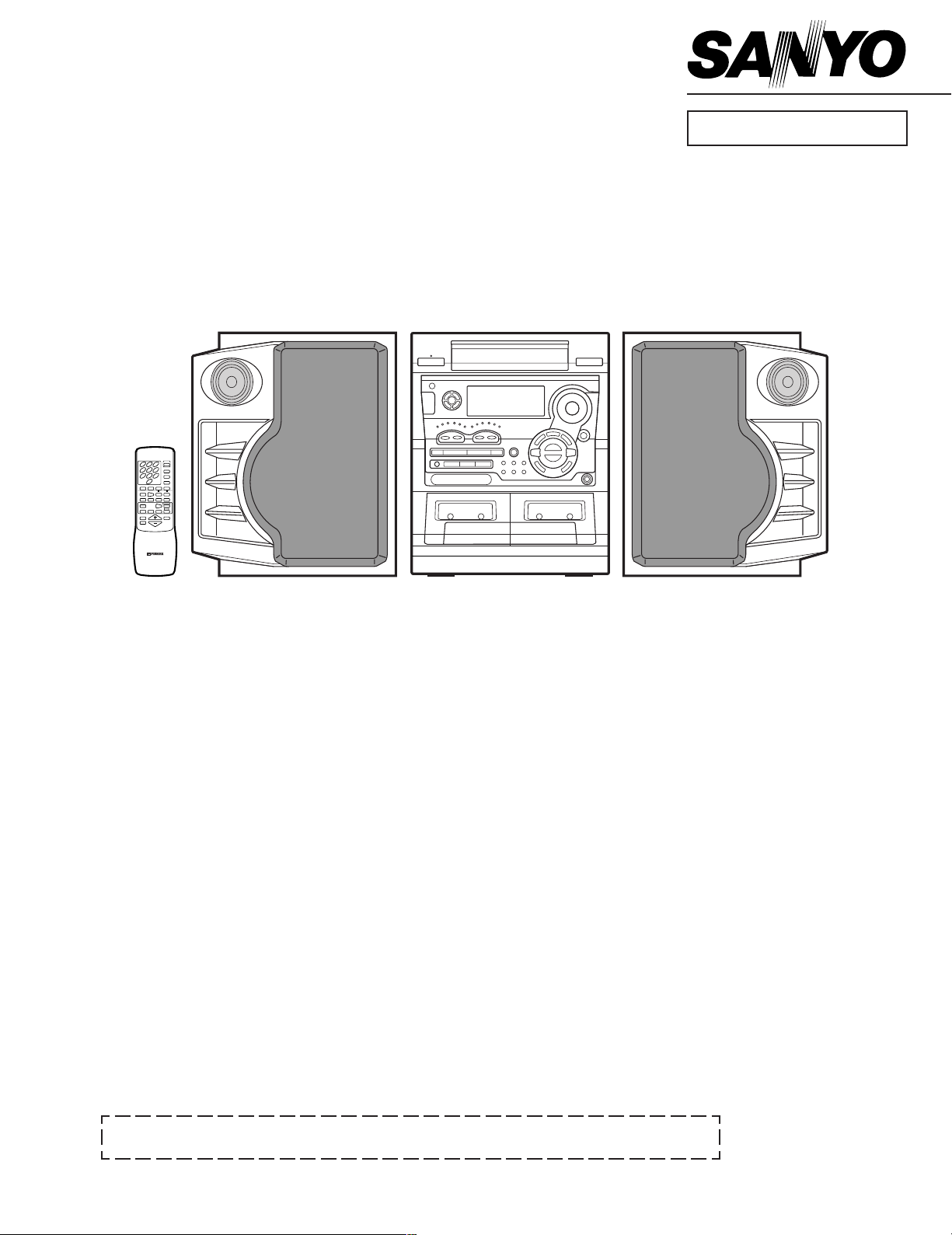
REMOTE CONTROL REM-C30
Micro Component System
DC-S800 (XE)
Contents
Specifications...................................................................1
What to do if.....................................................................1
Laser beam safety precaution.......................................... 2
CD pick-up maintenance.................................................. 2
Service mode ................................................................... 2
CD player adjustments..................................................... 3
Tape adjustments ............................................................4
Tuner adjustments ...........................................................6
Exploded view
(Cabinet & Chassis) ...................................................... 7
(Tape mechanism) ........................................................ 15
(CD changer mechanism) ............................................. 16
(CD base mechanism) ..................................................17
Parts list
(Cabinet & Chassis) ...................................................... 8
(Tape mechanism) ........................................................ 15
(CD mechanism) ...........................................................17
This service manual consists of "DC-S800U" (Main unit : 129 574 02), "RB-C30" (Remote control),
"SX-S800L" (Speaker system : 165 007 02) and "SX-S800R" (Speaker system : 165 008 02).
IC block diagram & description ........................................ 18
IC & Transistor voltages...................................................23
FL display description ...................................................... 24
Schematic diagram
(TUNER) ....................................................................... 26
(AMPLIFIER).................................................................28
(FRONT) ....................................................................... 34
(CD)...............................................................................38
(DECK)..........................................................................42
Wiring diagram
(TUNER & AMPLIFIER) ................................................30
(POWER TRANSFORMER) ........................................ 32
(HEADPHONE, LED & REGULATOR) .........................33
(FRONT) ....................................................................... 36
(CD)...............................................................................40
(DECK)..........................................................................41
(OPTICAL DIGITAL OUT & SUB TRANS )...................44
Wiring connection ............................................................45
PRODUCT CODE No.
129 575 02
REFERENCE No.
SM5810143
Page 2

This file was downloaded and provided FREE OF CHARGE
from the ManualDirectory community.
You can find many free to download Service Manuals & Schematics at
http://www.manualdirectory.co.uk
Page 3
SPECIFICATIONS
Tuner section
Reception frequency
(FM)
Frequency range.................... 87.5 MHz - 108 MHz
(MW)
Frequency range.................... 522 kHz - 1611 kHz
(LW)
Frequency range.................... 144 kHz - 288 kHz
Cassette deck section
Track system ......................... 4-track, 2-channel stereo
Frequency response .............. 120 Hz - 14 kHz
Signal to noise ratio ............... 48 dB
Wow and Flutter..................... 0.12 % (WRMS)
Fast forward / Rewind time .... Approx. 110 sec. (C-60)
General
Output power ......................... 100Wx2 (at 6ohm, 10% distortion)
Input
VIDEO/DVD IN .................... 550 mV/ 50 kohms
Outputs
Speakers.............................. 6 ohms
PHONES.............................. 8 - 32 ohms
OPTICAL DIGITAL OUT...... Optical
Power requirements............... AC 230V, 50Hz
Power consumption ............... 120 Watts
1.4W (Eco On standby mode)
Dimensions (W x H x D) ........ Approx.
270(W)x330(H)x317(D)mm
Weight.................................... Approx. 8.9kg
CD changer section
Type....................................... Changer, 3-disc
Channels................................ 2-channel stereo
Sampling frequency ............... 44.1 kHz
Pick-up................................... Optical 3-beam
semiconductor laser
Laser output........................... 0.6mW (Continuous wave max.)
Wave length........................... 790 nm
Wow and Flutter..................... Below measurable limits
WHAT TO DO IF
Speaker system
Type....................................... 3 way acoustic bass tube
United used............................ Woofer : 16 cm cone type
Mid range : 8 cm cone type
Tweeter : piezoelectric
Maximum
Power-handling capacity..... 180 Watts (peak)
Nominal impedance ............... 6 ohms
Dimensions (W x H x D) ........ Approx.
275(W) x 330(H) x 304(D)mm
Weight.................................... 5.6kg (per speaker)
Specifications subject to change without notice.
• If the operation of the unit or display is not normal, or you wish
to clear the contents of the memory.
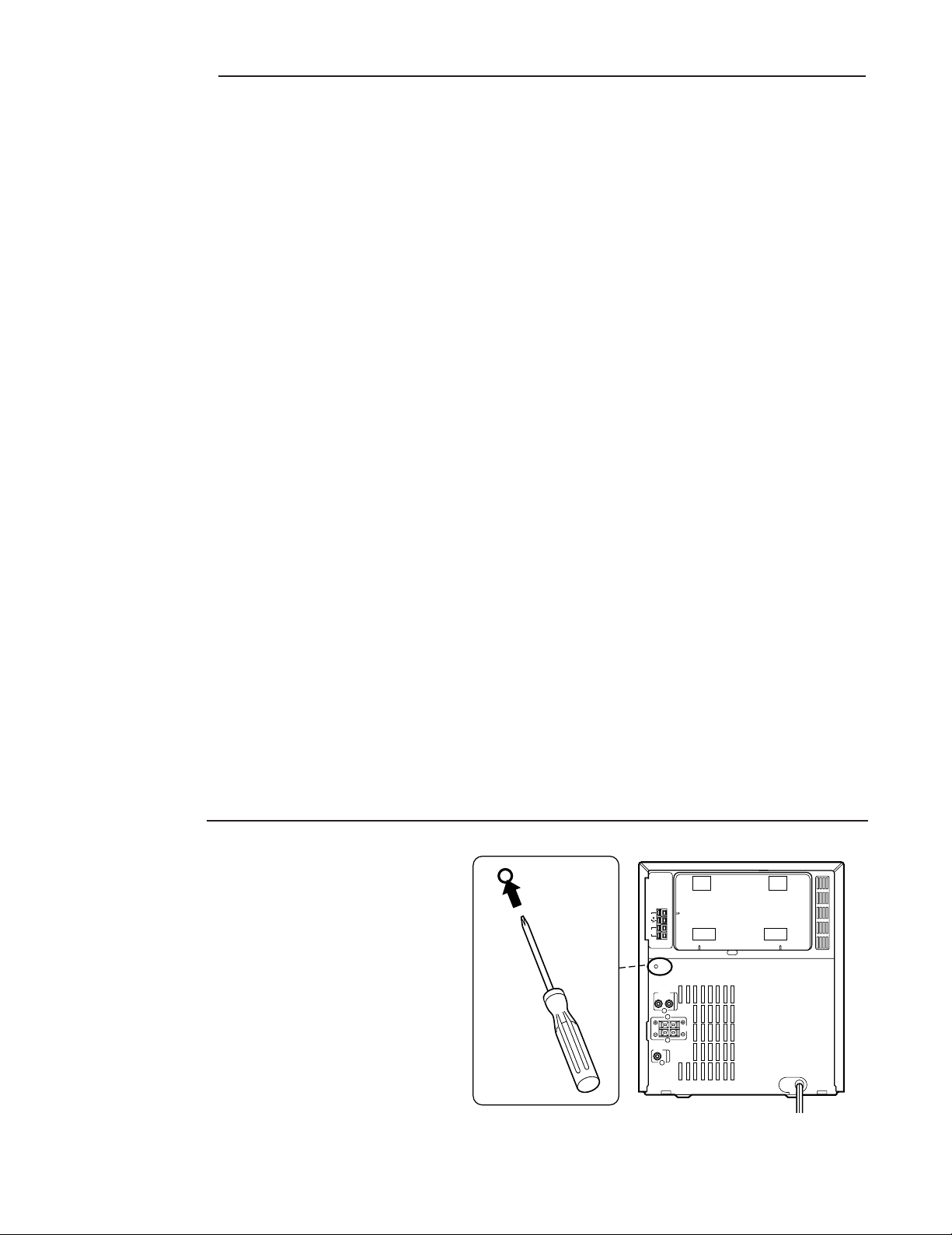
1. Disconnect the power cord from AC outlet.
2. Press the RESET button for at least 20 seconds.
3. Connect the power cord.
4. Press the POWER button to turn the power on.
- 1 -
RESET
FM
75
AM
LOOP
RESET
VIDEO/DVD
(AUDIO)
R
L
IN
R
L
SPEAKERS
(6ΩMIN.)
SUB WOOFER
Page 4
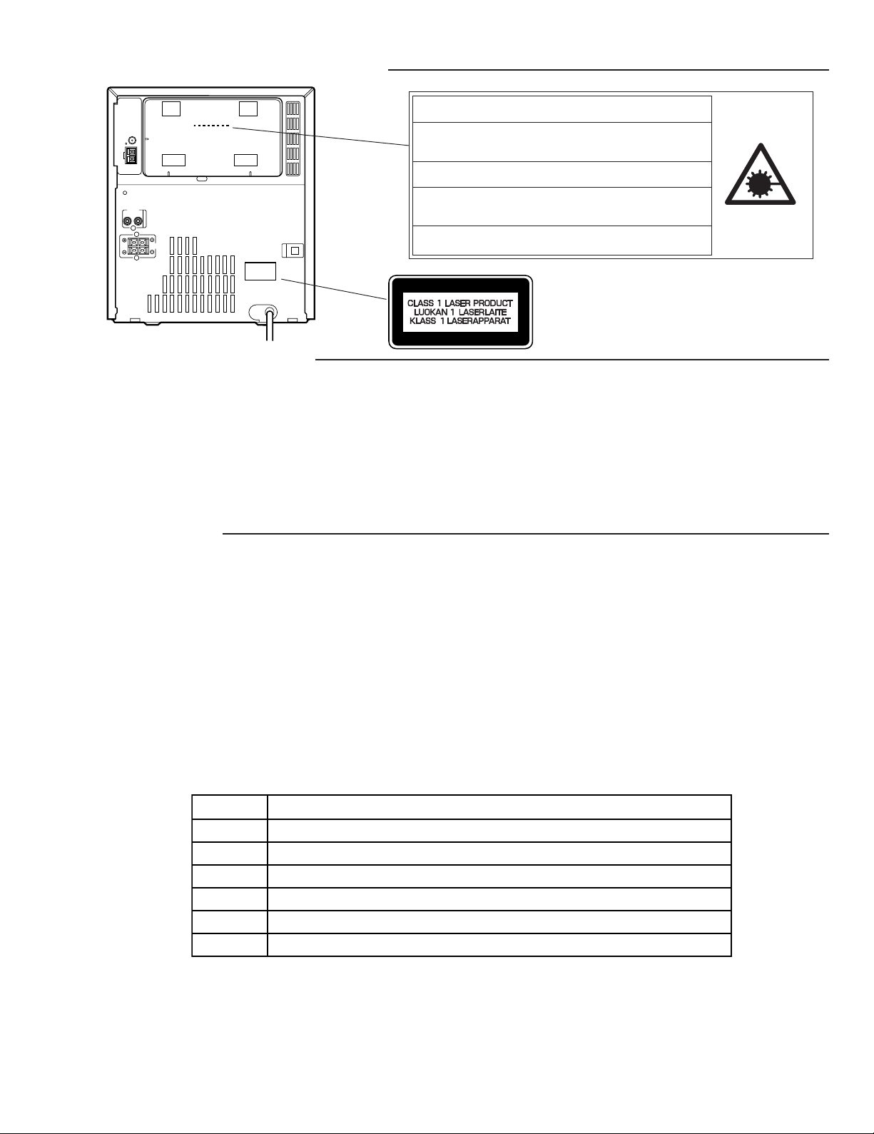
LASER BEAM SAFETY PRECAUTION
CAUTION – INVISIBLE LASER RADIATION WHEN OPEN AND
INTERLOCKS DEFEATED. AVOID EXPOSURE TO BEAM.
EXT.
ANT.
FM
75
AM
LOOP
ANT.
ADVARSEL – USYNLIG LASER STRÅLING VED ÅBNING, NÅR
SIKKERHEDSAFBRYDERE ER UDE AF FUNKTION, UNDGÅ UDS ÆTTELSE
FOR STRÅLING.
VARNING – OSYNLIG LASER STRÅLNING NÄR DENNA DEL ÄR ÖPPNAD
RESET
VIDEO/DVD
R
(AUDIO)
L
IN
R
L
SPEAKERS
(6ΩMIN.)
OUT
OPTICAL DIGITAL
OCH SPÄRR ÄR URKOPPLAD. STRÅLEN ÄR FARLIG.
VORSICHT – UNSICHTBARE LASERSTRAHLUNG TRITT AUS, WENN
DECKEL GEÖFFNET UND WENN SICHERHEITSVERRIEGELUNG
ÜBERBRÜCKT IST. NICHT, DEM STRAHL AUSSETZEN.
VARO – AVATTAESSA JA SUOJALUKITUS OHITETTAESSA OLET ALTTIINA
NÄKYMÄTTÖMÄLLE LASERSÄTEILYLLE. ÄLÄ KATSO SÄTEESEEN.
CD PICK-UP MAINTENANCE
About pick-up (Optical lens) Cleaning
Clean the lens with the specified cleaning disc or moisten a cotton swab with isopropyl alcohol and cleaning paper.
Specified cleaning disc : LC-1 (Part code : 645 026 1961 ..... manufactured by SANYO.)
Regarding procedure of cleaning with moisten cotton swab, please refer to the attached as follows.
1. Cotton swab wrapped with Cleaning paper.
2. Add the isopropyl alcohol.
3. Gently move the tip of cotton swab just like a draw a whirlpool from inside to outside on the surface of lens.
SERVICE MODE
1. Preparation
Press the unit's STOP and FM MODE buttons at the same time. (This initiates service mode entry status.)
Next, press another button on the unit to switch to the corresponding service mode.
The unit enters a service mode only if another button is pressed during that 1 second.
2. CD Repair
1. Within 1 second of activating service mode entry status, press the CD BACK button to enter this service mode.
2. When in the CD function mode the LCD segment displays a CD operation indication that is different from its normal indication.
If a CD error occurs, a display appears as shown in below.
Also, from the point at which the error occurred onward, the CD operation display is fixed. The fixed displays is canceled by
pressing the STOP button when the CD is stopped.
3. Press the POWER button to cancel this mode.
Disc No. State of CD Error
0 Good
1 Focusing is not possible in focus serch.
2 The subcode is not input during disc startup.
3 TOC can not be read.
4 Focus was lost while the servo was on. (during playing, etc.)
5 The subcode is not input while the servo in on. (during playing, etc.)
3. Checking the FL connection
1. Within 1 second of activating service mode entry status, press the TUNING UP button to enter this service mode.
2. FL and LED turns on order when enter this mode.
3. When every indication turns on, become on and off light indication.
4. Press the POWER button to cancel this mode.
- 2 -
Page 5
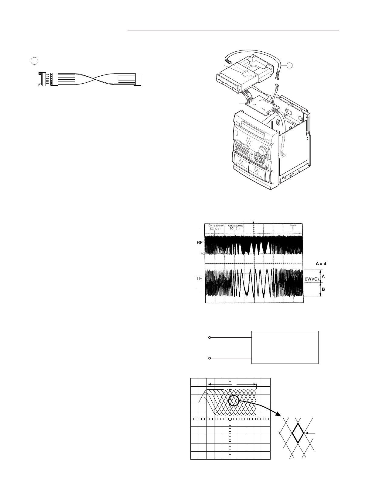
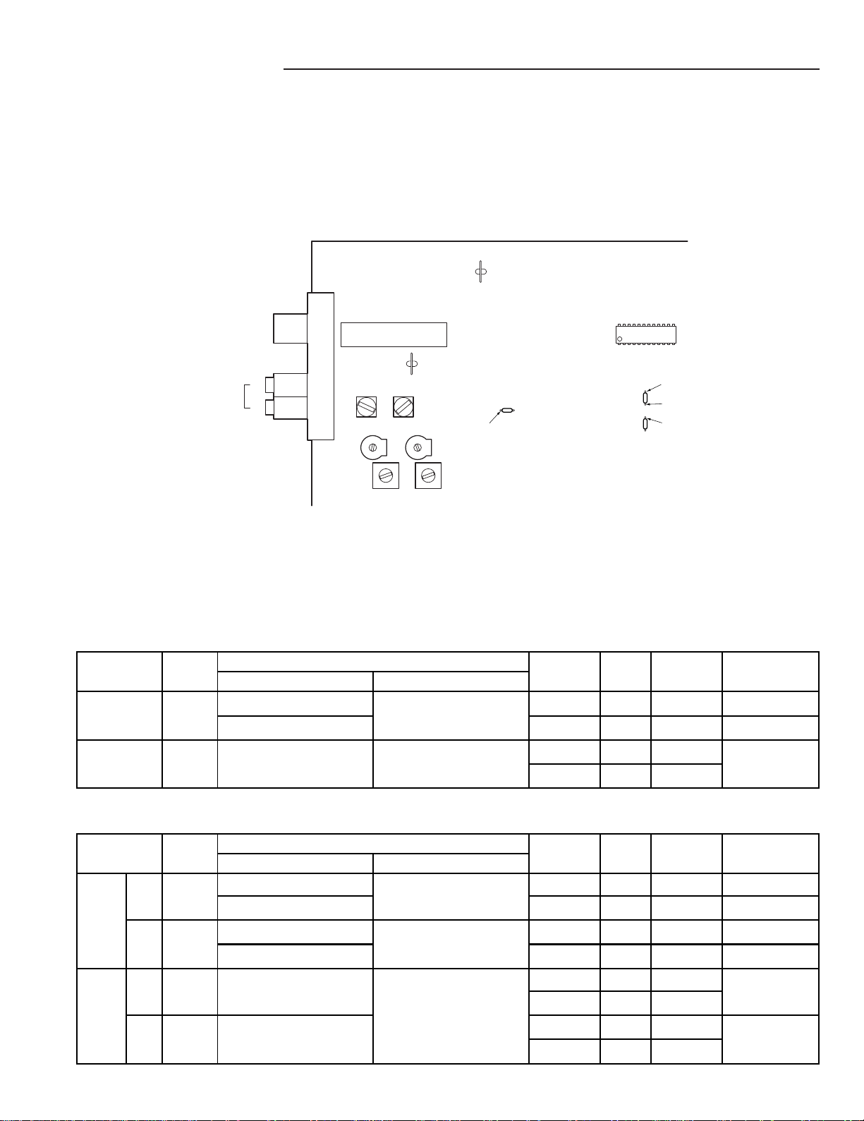
CD PLAYER ADJUSTMENTS
1. CABLE CONNECTION
1 ASSY, CONNECTOR-S (614 303 5633)
2. ADJUSTMENTS
(1) Confirm the tracking balance
1. Connect an Oscilloscope to TP2 (TE) and TP1 (VC).
2. Turn on the POWER switch.
3. Set the test disc. (DISC 1)
4. Press "STOP" button and "FM MODE" button simultaneously.
Within 1 second after pressing the "PLAY/PAUSE" button.
(SERVICE MODE : Tracking balance adjustment mode)
5. Confirm that the oscilloscope waveform is symmetrical on the
top and bottom in relation to 0V (VC).
SPINDLE / SLED
MOTOR P.W.B
CD P.W.B
1
CONNECTOR 6pin
(2) Checking the "eye" pattern
1. Switch "ON" the POWER.
2. Connect an oscilloscope to TP4 (RF) and TP1 (VC).
3. Load the test disc.
4. Press the PLAY button.
5. Check to be sure that the "eye" pattern is at the center of
waveform and that the diamond shape is clearly defined.
6. Press the STOP button.
7. Turn off the POWER switch.
- 3 -
200mV/div.
5ms/div.
TP4
(RF)
TP1
(VC)
+
OSCILLOSCOPE
-
a
OPENING EXPANDED
b
Page 6
TAPE ADJUSTMENTS
Adjustment Item Test Tape Measuring Output connection Adju st Adjus t
Instrument location value
(a) HEAD AZIMUTH VTT738 etc. AC-voltmeter SPEAKER TERMINAL HEAD AZIMUTH Max.
DECK "A" (10KHz) SCREW
(b) HEAD AZIMUTH VTT738 etc. AC-voltmeter SPEAKER TERMINAL HEAD AZIMUTH Max.
DECK "B" (10KHz) SCREW
(c) MOTOR SPEED MTT-111 FREQUENCY SPEAKER TERMINAL VR311 3,000Hz
(NORMAL) (3,000Hz) COUNTER
1. HEAD REPLACEMENT AND AZIMUTH ADJUSTMENT
(1) Head replacement
1. After replacement, demagnetize the heads by using a
degausser.
2. Be sure to clean the heads before attempting to make any
adjustments.
3. Be sure both channels (1 and 2) are the same level.
(Using a dual-channels oscilloscope).
4. All wiring should be returned to the original position after
work is completed.
(2) Head azimuth
• DECK "A"
1. Load a test tape (VTT-738,etc.: 10kHz) for azimuth
adjustment.
2. Press the PLAY button.
3. Use a flat-tip (-) screwdriver to turn the screw for normal
azimuth adjustment so that the left and right outputs are
maximized at the same phase during normal playback.
4. Press the STOP button.
TAPE ’’A’’
PLAY HEAD
EARTH
RED
WHITE
YELLOW
TAPE ’’B’’
R/P HEAD
RED
WHITE
EARTH
E. HEAD
YELLOW
ORANGE
• DECK "B"
1. Load a test for azimuth adjustment.
2. Press the PLAY button.
3. Azimuth screw adjustment.
4. Press the STOP button.
REVERSE
NORMAL
TAPE "A"
REVERSE
NORMAL
TAPE "B"
• After making the adjustment, secure the azimuth
adjustment screw by applying screw lock (TB-1401B).
- 4 -
Page 7
TAPE ADJUSTMENTS
2. MOTOR REPLACEMENT AND SPEED ADJUSTMENT
(1) Motor replacement
(2) Motor speed
1. Insert the test tape (MTT-111 or etc. 3,000 Hz) into DECK A.
2. Press the PLAY button.
3. Adjust VR311 so that the frequency counter show a reading
of 3,000 ± 10 Hz.
4. Press the STOP button.
3. CHECKING THE MECHANISM TORQUES
• Clean the head, capstan and pinch roller before making any measurement.
DECK " A & B"
Measureent Take-up torque Back tension Tape tension
Cassette for PLAY : TW-2111A PLAY : TW-2111A Drive-power cassette
measurement F.FWD/REW : TW-2231 TW-2412
PLAY 25 ~ 63 gr.cm 2.0 ~ 6.0 gr.cm 70 gr or more
F.FWD/REW 60 ~ 120 gr.cm - -
TAPE SPEED
ADJUSTMENT
VR311
- 5 -
Page 8
TUNER ADJUSTMENTS
o
o
o
• Use a plastic screw driver for adjustments.
• MODE : STEREO
• Speaker impedance : 6 ohm
• TUNING
FM : 87.5 - 108.0MHz (50kHz step)
MW : 522 - 1611kHz (9kHz step)
LW : 144 - 288kHz (9kHz step)
FM ANT 75ohm
COAXIAL CABLE
AM LOOP
ANT
(E)
(H)
CN201
L2154
L2153
CT251 CT252
TP11
(COVER V)
J2110
TP12
(E)
J2102
R2303
R2325
R2326
TP25
(L CH)
TP27
(E)
TP26
(R CH)
L2151
L2152
SG RF Level : 75 open Voltage dBµV
Antenna : 75 unbalanced , Modulation : 1 kHz
1.FM
Step Adjusting
Circuit
1 Cover --- Connect Digital DC voltmeter t
voltage --- TP11(H), TP12(E). 108.0 MHZ High --- less than 9.0V
2 Cover Connect FM SG to FM Antenn Connect to VTVM 90.0 MHZ Low ---
voltage
Input Output
SG≒8dBμV
Dev. : ±22.5kHz(MONO) ±22.5kHz(STEREO) ±6.75kHz(PILOT)
Connection
TP25(L) or TP26(R), TP27(E) 106.0 MHZ High ---
SG Set Adjustment Remark
Frequency Position
87.5 MHZ Low --- more than 0.9V
SG Modulation : 1kHz, 30%
2.AM
Step Adjusting
Circuit
MW Cover --- Connect Digital DC voltmeter t
1 voltage --- TP11(H), TP12(E). 1611 kHZ High --- less than 9.0V
Input Output
Antenna, IRE Loop, Distance: 60 cm
Connection
SG Set Adjustment Remark
Frequency Position
522 kHZ Low L2153
1.0V±0.05V
LW Cover --- Connect Digital DC voltmeter t
144 kHZ Low L2154
voltage --- TP11(H), TP12(E). 288 kHZ High --- less than 9.0V
M W Tracking Connect AM SG to Loop Ant. Connect to VTVM 603 kHZ Low L2152 Max.
2
SG≒80dBμV
TP25(L) or TP26(R), TP27(E). 1404 kHZ High CT252
LW Tracking Connect AM SG to Loop Ant. 162 kHZ Low L2151 Max.
SG≒85dBμV
279 kHZ High CT251
- 6 -
1.0V±0.05V
Page 9
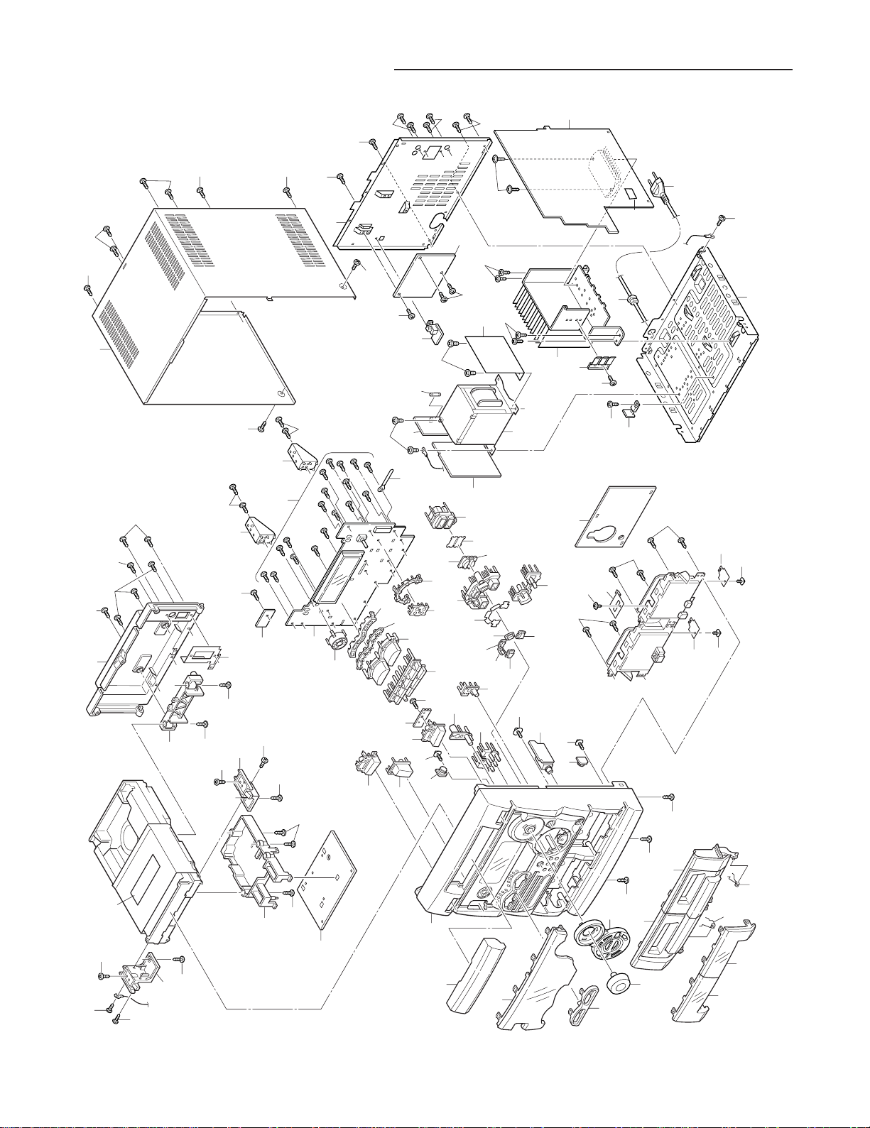
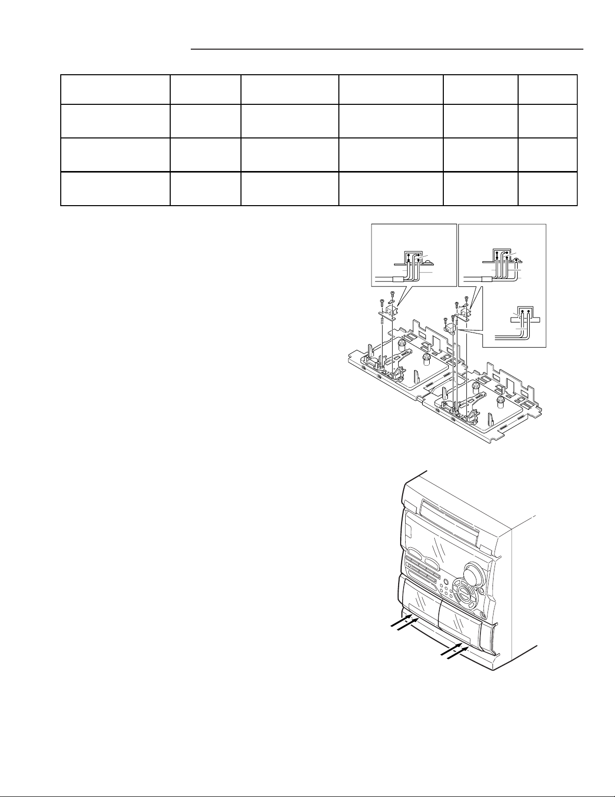
EXPLODED VIEW (CABINET & CHASSIS)
49
Y20
Y20
Y29
Y29
Y20
Y20
Y20
Y20
Y20
50
53
64
52
66
Y21
Y22
Y22
Y22
Y21
48
Y19
Y17
Y17
Y18
Y16
Y16
Y11
Y12
Y13
9
1
7
8
10
11
12
15
15
13
13
14
42
42
45
43
54
44
46
Y11
Y12
Y15
Y13
Y14
Y15
Y02
Y02
Y02
Y03
Y03
Y03
Y25
Y24
Y25
Y28
Y27
Y26
Y10
Y10
Y04
Y05
Y04
Y01
Y01
Y01
75
71
72
78
80
81
79
63
61
Y23
Y23
76
77
62
51
2
3
4
5
6
16
17
18
19
21
20
22
23
24
25
26
27
28
29
30
31
32
33
34
35
36
37
39
38
40
41
47
73
74
Y07
Y08
Y06
Y09
55
- 7 -
Page 10

PARTS LIST
PRODUCT SAFETY NOTICE
EACH PRECAUTION IN THIS MANUAL SHOULD BE FOLLOWED DURING SERVICING. COMPONENTS IDENTIFIED WITH THE IEC
!!
SYMBOL
SPECIAL SIGNIFICANCE. WHEN REPLACING A COMPONENT IDENTIFIED BY
OR PARTS WITH THE SAME RATINGS OF RESISTANCE, WATTAGE OR VOLTAGE THAT ARE DESIGNATED IN THE PARTS LIST
IN THIS MANUAL. LEAKAGE-CURRENT OR RESISTANCE MEASUREMENTS MUST BE MADE TO DETERMINE THAT EXPOSED
PARTS ARE ACCEPTABLY INSULATED FROM THE SUPPLY CIRCUIT BEFORE RETURNING THE PRODUCT TO THE CUSTOMER.
CAUTION : Regular type resistors and capacitors are not listed. To know those values, refer to the schematic diagram.
!
IN THE PARTS LIST AND THE SCHEMATIC DIAGRAM DESIGNATED COMPONENTS IN WHICH SAFETY CAN BE OF
!!
!
, USE ONLY THE REPLACEMENT PARTS DESIGNATED,
Regular type resistors are less than 1/4 W carbon type and 0 ohm chip resistors.
Regular type capacitors are less than 50 V and less than 1000 µF type of Ceramic type and Electrical type.
PACKING & ACCESSORIES
REF.NO. PART NO. DESCRIPTION
614 310 6234 CARTON CASE
614 308 7663 CUSHION,TOP
614 308 7670 CUSHION,BOTTOM
614 271 6656 CUSHION,SET
614 310 6241 INSTRUCTION MANUAL
614 312 3231 INSTRUCTION MANUAL,GREEK
645 005 1227 ASSY,ANTENA,LOOP
614 308 5515 ANT,FM ANT
or 614 229 4635 ANT,FM ANT
645 034 1571 REMOCON,RB-C30ARD,SANYO
645 035 8098 BATTERY COVER,SERVICE PARTS
CABINET & CHASSIS
REF.NO. PART NO. DESCRIPTION
1 614 308 7335 DEC,WINDOW,CAS,L
2 614 308 7342 DEC,WINDOW,CAS,R
3 614 310 6081 LID,CASSETTE,L,AUTO REVERSE
4 614 308 7410 LID,CASSETTE,R
5 614 308 7526 SPRING,WIRE,LID CASSETTE L
6 614 308 7533 SPRING,WIRE,LID CASSETTE R
7 614 308 7397 KNOB,ROTARY
8 614 308 7199 DEC,VOL
9 614 308 7205 DEC,BASS
10 614 312 1480 DEC,WINDOW,FL,BASS XPANDER
11 614 308 7212 DEC,CD,TRAY
12 614 310 6043 ASSY,CABINET,FRONT
13 614 289 1117 MOUNTING,BRACKET,
DECK MECHA BOTTOM
14 614 289 1100 MOUNTING,BRACKET,
DECK MECHA TOP
15 614 309 7969 ASSY,GEAR,(SESK)
16 614 308 7083 BUTTON,SOUND
17 614 308 7069 BUTTON,POWER
18 614 308 7076 BUTTON,CD,OPEN
20 614 308 7106 BUTTON,CLOCK
21 614 308 7137 BUTTON,REC
22 614 308 7168 BUTTON,FUNCTION
23 614 310 3820 BUTTON,TAPE,AUTO REVERSE
24 614 308 7090 BUTTON,BASS
25 614 308 7243 DEC,WINDOW,BASS
26 614 308 7489 REFLECTOR,BASS
27 614 308 7472 REFLECTOR,SOUND
28 614 308 7519 REFLECTOR,CD
29 614 308 7502 REFLECTOR,DISC
30 614 308 7298 DEC,WINDOW,CD,REW
31 614 308 7304 DEC,WINDOW,CD,FF
32 614 308 7267 DEC,WINDOW,DISC,1
33 614 308 7274 DEC,WINDOW,DISC,2
34 614 308 7281 DEC,WINDOW,DISC,3
REF.NO. PART NO. DESCRIPTION
35 614 308 7366 DEC,SHEET,DISC
36 614 308 7120 BUTTON,DISC
37 614 308 7151 BUTTON,MEMORY
38 614 308 7311 DEC,WINDOW,CD,PLAY
39 614 308 7328 DEC,WINDOW,CD,STOP
40 614 308 7373 DEC,SHEET,CD
41 614 308 7144 BUTTON,CD
42 614 301 6533 MOUNTING,CD,FRONT,
FRONT/CD MECHA
43 614 301 6526 MOUNTING,CD,RIGHT,
FRONT/CD MECHA
44 614 301 6519 MOUNTING,CD,LEFT,
FRONT/CD MECHA
45 614 300 3113 COVER PICK,CD PICK COVER
46 614 302 1834 MOUNTING,CD,REAR,
PANEL REAR/CD MECHA
47 614 302 1902 TERMINAL,ANT,PANEL REAR/ANT
48 614 309 8614 PANEL,REAR,CD MECHA
49 614 310 6470 ASSY,CABINET,AFTER BENDING
50 614 310 3868 PANEL,REAR
52 614 129 1901 FIXER,AC CORD
or 614 284 1884 FIXER,AC CORD
53 614 290 4954 ASSY,CABINET,BOTTOM
54 614 274 8190 LABEL,SAFETY,LASER
55 614 225 8569 STAND,MAIN PWB
FIXING PARTS
REF.NO. PART NO. DESCRIPTION
Y01 411 021 3503 SCR S-TPG BIN 3X10,BOTTOM/FRONT
Y02 411 024 3708 SCR S-TPG PAN+FLG 2X6,
DECK MECHA/MOUNTING PWB
Y03 411 021 3503 SCR S-TPG BIN 3X10,DECK MECHA
Y04 412 003 1708 SPECIAL SCREW,GEAR CASSETTE
Y05 412 032 6408 SPECIAL SCREW,HEAD PHONE
Y07 614 129 9136 LUG,CN423 FIX
Y08 411 021 3503 SCR S-TPG BIN 3X10,FRONT PWB
Y09 411 021 3503 SCR S-TPG BIN 3X10,SUB PWB
Y10 411 021 3503 SCR S-TPG BIN 3X10,
MOUNTING CD FRONT
Y11 411 021 3503 SCR S-TPG BIN 3X10,
CD MECHA/COVERPICK
Y12 411 021 3503 SCR S-TPG BIN 3X10,
MOUNING FRONT/MOUNTING L
Y13 411 021 1806 SCR S-TPG BIN 2.6X10,
CD MECHA/MOUNTING L,R(SI
Y14 411 027 3101 SCR S-TPG BIN 3X8,CD PWB GRAND
Y15 411 021 3503 SCR S-TPG BIN 3X10,
CD MECHA/MOUNTING L,R(BT
Y16 411 021 3503 SCR S-TPG BIN 3X10,
CD MECHA/MOUNTING REAR
- 8 -
Page 11

PARTS LIST
REF.NO. PART NO. DESCRIPTION
Y17 411 021 3701 SCR S-TPG BIN 3X10,
CD MECHA/REAR
Y18 411 021 3701 SCR S-TPG BIN 3X10,REAR/REAR
Y19 411 021 3701 SCR S-TPG BIN 3X10,
REAR/ELECT PARTS
Y20 411 021 3701 SCR S-TPG BIN 3X10,CABINET TOP
Y21 411 021 3701 SCR S-TPG BIN 3X10,
BOTTOM/PANEL REAR(PAF002
Y23 411 001 3905 SCR S-TPG BIN 4X6,TRANS
Y24 411 020 9506 SCR S-TPG BRZ+FLG 3X16,
POWER AMP 1
Y25 411 021 3503 SCR S-TPG BIN 3X10,
BOTTOM/HEAT SINK
Y26 411 021 3503 SCR S-TPG BIN 3X10,TR HOLDER
Y27 411 021 6405 SCR S-TPG BIN 3X8,POWER IC
Y28 411 021 6405 SCR S-TPG BIN 3X8,AMP-GND
Y29 411 021 3503 SCR S-TPG BIN 3X10,
REAR/SUB TRANS PWB
ELECTRICAL PARTS
REF.NO. PART NO. DESCRIPTION
61
62
63
64
or
65 614 305 6768 SHIELD,TRANS,PT SHIELD
66
CN381 614 308 0206 ASSY,WIRE,DECK A
or 614 304 7896 ASSY,WIRE,DECK A
CN382 614 308 0190 ASSY,WIRE,DECK B
or 614 303 6388 ASSY,WIRE,DECK B
CN383
CN384 645 028 5509 FLEXIBLE FLAT CABLE,FRONT-DECK
CN681 645 041 1793 FLEXIBLE FLAT CABLE,CD
CN682 614 304 8596 ASSY,WIRE,CD
or 614 302 2107 ASSY,WIRE,CD
CN683 614 312 2586 ASSY,WIRE,CD-DIGITAL OUT
CN691 645 013 7907 FLEXIBLE FLAT CABLE,FRONT-CD
LUG01
LUG02
SA404 411 001 3905 SCR S-TPG BIN 4X6,FOR LUG
SA405 411 021 5705 SCR S-TPG BIN 3X6,FOR LUG
!!
!
423 016 7809 FUSE 250V 2A
!!
!
645 033 8540 POWER TRANSFORMER
!!
!
614 310 5619 ASSY,HEAT SINK
!!
!
645 016 9939 CORD,POWER-1.74MK,FOR XE/PA
!!
!
614 255 2513 POWER CORD,FOR XE/PA
!!
!
614 291 6568 MOUNTING,PWB,TR HOLDER
!!
!
645 041 2356 FLEXIBLE FLAT CABLE,AMP-DECK
!!
!
614 130 0382 LUG
!!
!
614 130 0382 LUG
!!
!
614 086 2164 COVER,CAPACITOR(C4316)
DECK P.W.BOARD ASSY
REF.NO. PART NO. DESCRIPTION
71 614 306 5357 ASSY,PWB,DECK (Only Initial)
C3606 403 061 7306 POLYESTER 4700P J 50V
C3607 403 061 9607 POLYESTER 0.047U J 50V
CN301 645 012 5089 SOCKET,FPC 10P
or 645 005 4181 SOCKET,10P
CN302 645 012 5096 SOCKET,FPC 12P
or 645 005 4204 SOCKET,12P
CN311 614 035 4959 SOCKET,DIP 6P
or 645 012 7823 SOCKET,DIP 6P
CN312 614 020 6562 SOCKET,4P
or 614 223 9223 SOCKET
CN313 645 012 2729 SOCKET,DIP 7P
or 645 012 7830 SOCKET,DIP 7P
CN321 614 303 6647 CORD,6P CONNECTOR,A_MECHA
or 614 308 0336 CORD,6P CONNECTOR,A_MECHA
CN323 614 303 6654 CORD,7P CONNECTOR,B_MECHA
or 614 308 0343 CORD,7P CONNECTOR,B_MECHA
REF.NO. PART NO. DESCRIPTION
CN371 645 005 7373 PLUG,3P
or 645 007 0068 PLUG,3P
CN372 645 005 8127 PLUG,6P
or 645 007 0099 PLUG,6P
CN373 645 005 8226 PLUG,3P
or 645 009 6433 PLUG,3P
CN374 614 305 6317 CORD,1P CONNECTOR
!!
D3101
D3102
!
407 148 6701 DIODE 1A3-I
!!
!
407 148 6701 DIODE 1A3-I
D3601 407 099 5105 ZENER DIODE MTZJ4.7B
D3621 407 012 4406 DIODE 1SS133
D3622 407 012 4406 DIODE 1SS133
D3623 407 012 4406 DIODE 1SS133
D3624 407 012 4406 DIODE 1SS133
HS301 614 215 9347 HEAT SINK
HS302 614 215 9347 HEAT SINK
IC361 409 346 2301 IC BU2090F
IC362 409 050 8200 IC TC4011BF
IC363 409 189 3404 IC BA7755A
IC371 409 251 1000 IC TA8189N
L3601 645 032 5823 TRANS,OSC,85KHZ
L3701 645 004 0580 INDUCTOR,1M J
L3801 645 004 0580 INDUCTOR,1M J
Q3122 405 141 3703 TR KTA1271-Y
or 405 008 2405 TR 2SB698-F
or 405 008 2504 TR 2SB698-G
or 405 006 3909 TR 2SA952-K
or 405 006 4005 TR 2SA952-L
Q3124 405 141 3703 TR KTA1271-Y
or 405 008 2405 TR 2SB698-F
or 405 008 2504 TR 2SB698-G
or 405 006 3909 TR 2SA952-K
or 405 006 4005 TR 2SA952-L
Q3125 405 141 3703 TR KTA1271-Y
or 405 008 2405 TR 2SB698-F
or 405 008 2504 TR 2SB698-G
or 405 006 3909 TR 2SA952-K
or 405 006 4005 TR 2SA952-L
Q3601 405 141 3703 TR KTA1271-Y
or 405 008 2405 TR 2SB698-F
or 405 008 2504 TR 2SB698-G
or 405 006 3909 TR 2SA952-K
or 405 006 4005 TR 2SA952-L
Q3602 405 143 8706 TR KTC3199-GR
or 405 011 8609 TR 2SC1740S-S
or 405 011 8500 TR 2SC1740S-R
or 405 017 9600 TR 2SC3330-T
or 405 017 9709 TR 2SC3330-U
Q3603 405 141 3307 TR KTC3198-GR
or 405 141 3208 TR KTC3198-Y
or 405 019 3804 TR 2SC536-G-NP
or 405 019 2708 TR 2SC536-F-NP
Q3605 405 151 4905 TR KTC3200-GR
or 405 151 5001 TR KTC3200-BL
or 405 011 1907 TR 2SC1627-Y
or 405 012 8103 TR 2SC2003-L
or 405 137 6404 TR 2SC2003-K
Q3611 405 109 9204 TR KRC102M-A
or 405 000 3103 TR DTC114ES
or 405 078 3005 TR BA1L4M
Q3621 405 109 9402 TR KRC111M
or 405 000 3400 TR DTC114TS
Q3622 405 109 9204 TR KRC102M-A
or 405 000 3103 TR DTC114ES
or 405 078 3005 TR BA1L4M
Q3701 405 109 9402 TR KRC111M
or 405 000 3400 TR DTC114TS
- 9 -
Page 12

PARTS LIST
REF.NO. PART NO. DESCRIPTION
Q3702 405 095 2708 TR 2SJ40-D
or 405 095 2807 TR 2SJ40-E
or 405 149 6003 TR 2SJ498
or 405 085 9106 TR 2SJ105-GR
or 405 095 3408 TR 2SJ105-BL
Q3703 405 095 2708 TR 2SJ40-D
or 405 095 2807 TR 2SJ40-E
or 405 149 6003 TR 2SJ498
or 405 085 9106 TR 2SJ105-GR
or 405 095 3408 TR 2SJ105-BL
Q3704 405 109 9204 TR KRC102M-A
or 405 000 3103 TR DTC114ES
or 405 078 3005 TR BA1L4M
Q3801 405 109 9402 TR KRC111M
or 405 000 3400 TR DTC114TS
Q3802 405 095 2708 TR 2SJ40-D
or 405 095 2807 TR 2SJ40-E
or 405 149 6003 TR 2SJ498
or 405 085 9106 TR 2SJ105-GR
or 405 095 3408 TR 2SJ105-BL
Q3803 405 095 2708 TR 2SJ40-D
or 405 095 2807 TR 2SJ40-E
or 405 149 6003 TR 2SJ498
or 405 085 9106 TR 2SJ105-GR
or 405 095 3408 TR 2SJ105-BL
Q3804 405 109 9204 TR KRC102M-A
or 405 000 3103 TR DTC114ES
or 405 078 3005 TR BA1L4M
R3608 401 011 4900 CARBON 82 JA 1/2W
VR311 645 003 5685 VR,SEMI,2.2K N
HEADPHONE P.W.BOARD ASSY
REF.NO. PART NO. DESCRIPTION
72 614 310 6838 ASSY,PWB,HEADPHONE (Only Initial)
CN422 645 009 0042 JACK,PHONE D6.43
CN432 645 005 8110 PLUG,4P
FRONT P.W.BOARD ASSY
REF.NO. PART NO. DESCRIPTION
73 614 310 6821 ASSY,PWB,FRONT (Only Initial)
BR601 614 308 7380 HOLDER,FL,FL_MOUNT
C6095 403 291 5608 ELECT 1000U M 6.3V
CN601 645 032 5809 PLUG,22P,FRONT-PRE
CN602 614 035 4935 SOCKET,DIP 4P
or 645 012 7809 SOCKET,DIP 4P
CN603 645 012 5249 SOCKET,FPC 20P
or 645 005 4280 SOCKET,20P
CN604 645 012 5096 SOCKET,FPC 12P
or 645 005 4204 SOCKET,12P
CN607 614 035 4911 SOCKET,DIP 2P
CN612 614 308 0329 CORD,4P CONNECTOR,FRONT-PT2
or 614 303 6623 CORD,4P CONNECTOR,FRONT-PT2
D6001 407 012 4406 DIODE 1SS133
D6004 407 012 4406 DIODE 1SS133
D6007 407 099 4603 ZENER DIODE MTZJ3.9B
D6202 408 039 4400 LED SLZ-981B-09H-AB-T1,
SOUND_PRESET_LED
D6203 408 036 0504 LED SLZ-381C-09H-AB-T1,
SOUND_LED
D6204 408 037 4204 LED SLP-3118B-51HAB-T1,
BASS_PASS_LED
D6205 408 037 4204 LED SLP-3118B-51HAB-T1,
BASS_PASS_LED
REF.NO. PART NO. DESCRIPTION
D6206 408 037 4204 LED SLP-3118B-51HAB-T1,
BASS_PASS_LED
D6208 408 037 4204 LED SLP-3118B-51HAB-T1,
BASS_PASS_LED
D6210 408 037 4204 LED SLP-3118B-51HAB-T1,
BASS_PASS_LED
D6212 408 037 4204 LED SLP-3118B-51HAB-T1,
BASS_PASS_LED
D6214 408 039 4400 LED SLZ-981B-09H-AB-T1,
SOUND_PRESET_LED
D6216 408 039 4400 LED SLZ-981B-09H-AB-T1,
SOUND_PRESET_LED
D6217 408 039 4400 LED SLZ-981B-09H-AB-T1,
SOUND_PRESET_LED
D6301 408 043 2607 LED SLZ-336A-14H-AB-T2,DISC_LED
D6302 408 043 2607 LED SLZ-336A-14H-AB-T2,DISC_LED
D6303 408 043 2607 LED SLZ-336A-14H-AB-T2,DISC_LED
D6304 408 043 2607 LED SLZ-336A-14H-AB-T2,DISC_LED
D6305 408 043 2607 LED SLZ-336A-14H-AB-T2,DISC_LED
D6306 408 043 2607 LED SLZ-336A-14H-AB-T2,DISC_LED
D6307 408 043 2607 LED SLZ-336A-14H-AB-T2,DISC_LED
D6308 408 043 2607 LED SLZ-336A-14H-AB-T2,DISC_LED
D6309 408 043 2607 LED SLZ-336A-14H-AB-T2,DISC_LED
DS601 407 217 1101 PHOTO DIODE SPS-442-1G,IR
FL601 645 040 1220 FLOURESCENT TUBE,FL
IC601 410 377 5100 IC LC866556B-5R77,MICOM
IC602 409 426 1903 IC KIA4558F,OP_AMP
or 409 039 7804 IC NJM4558M,OP_AMP
IC604 409 346 2301 IC BU2090F,LED_DRIVER
IC605 409 346 2301 IC BU2090F,LED_DRIVER
L6000 645 001 4550 INDUCTOR,10U K
or 645 031 7835 INDUCTOR,10U K
Q6001 405 143 8706 TR KTC3199-GR
or 405 017 9600 TR 2SC3330-T
or 405 017 9709 TR 2SC3330-U
or 405 011 8500 TR 2SC1740S-R
or 405 011 8609 TR 2SC1740S-S
Q6002 405 143 6504 TR KTA1267-GR
or 405 004 4601 TR 2SA608-F-SPA
or 405 004 5103 TR 2SA608-G-SPA
or 405 006 1806 TR 2SA933S-R
or 405 006 1905 TR 2SA933S-S
Q6003 405 141 3703 TR KTA1271-Y
or 405 008 2405 TR 2SB698-F
or 405 008 2504 TR 2SB698-G
Q6005 405 143 8706 TR KTC3199-GR
or 405 017 9600 TR 2SC3330-T
or 405 017 9709 TR 2SC3330-U
or 405 011 8500 TR 2SC1740S-R
or 405 011 8609 TR 2SC1740S-S
Q6006 405 143 8706 TR KTC3199-GR
or 405 017 9600 TR 2SC3330-T
or 405 017 9709 TR 2SC3330-U
or 405 011 8500 TR 2SC1740S-R
or 405 011 8609 TR 2SC1740S-S
Q6007 405 110 5400 TR KRA102M-A
or 405 000 0508 TR DTA114ES
Q6008 405 143 6504 TR KTA1267-GR
Q6202 405 110 5400 TR KRA102M-A
or 405 000 0508 TR DTA114ES
Q6203 405 110 5400 TR KRA102M-A
or 405 000 0508 TR DTA114ES
Q6204 405 110 5400 TR KRA102M-A
or 405 000 0508 TR DTA114ES
Q6205 405 110 5400 TR KRA102M-A
or 405 000 0508 TR DTA114ES
- 10 -
Page 13

PARTS LIST
REF.NO. PART NO. DESCRIPTION
Q6206 405 110 5400 TR KRA102M-A
or 405 000 0508 TR DTA114ES
Q6208 405 110 5400 TR KRA102M-A
or 405 000 0508 TR DTA114ES
Q6210 405 110 5400 TR KRA102M-A
or 405 000 0508 TR DTA114ES
Q6212 405 110 5400 TR KRA102M-A
or 405 000 0508 TR DTA114ES
Q6214 405 110 5400 TR KRA102M-A
or 405 000 0508 TR DTA114ES
Q6216 405 110 5400 TR KRA102M-A
or 405 000 0508 TR DTA114ES
Q6217 405 110 5400 TR KRA102M-A
or 405 000 0508 TR DTA114ES
Q6302 405 110 5400 TR KRA102M-A
or 405 000 0508 TR DTA114ES
Q6303 405 110 5400 TR KRA102M-A
or 405 000 0508 TR DTA114ES
Q6305 405 110 5400 TR KRA102M-A
or 405 000 0508 TR DTA114ES
Q6306 405 110 5400 TR KRA102M-A
or 405 000 0508 TR DTA114ES
Q6307 405 110 5400 TR KRA102M-A
or 405 000 0508 TR DTA114ES
Q6308 405 110 5400 TR KRA102M-A
or 405 000 0508 TR DTA114ES
Q6309 405 110 5400 TR KRA102M-A
or 405 000 0508 TR DTA114ES
S6001 645 033 3460 SWITCH,ROTARY(ENCODER),VOL
S6100 614 240 1002 SWITCH,TACT
or 645 006 5958 SWITCH,PUSH 1P-1T
or 614 220 5471 SWITCH,TACT
S6101 614 240 1002 SWITCH,TACT
or 645 006 5958 SWITCH,PUSH 1P-1T
or 614 220 5471 SWITCH,TACT
S6102 614 240 1002 SWITCH,TACT
or 645 006 5958 SWITCH,PUSH 1P-1T
or 614 220 5471 SWITCH,TACT
S6103 614 240 1002 SWITCH,TACT
or 645 006 5958 SWITCH,PUSH 1P-1T
or 614 220 5471 SWITCH,TACT
S6104 614 240 1002 SWITCH,TACT
or 645 006 5958 SWITCH,PUSH 1P-1T
or 614 220 5471 SWITCH,TACT
S6105 614 240 1002 SWITCH,TACT
or 645 006 5958 SWITCH,PUSH 1P-1T
or 614 220 5471 SWITCH,TACT
S6106 614 240 1002 SWITCH,TACT
or 645 006 5958 SWITCH,PUSH 1P-1T
or 614 220 5471 SWITCH,TACT
S6107 614 240 1002 SWITCH,TACT
or 645 006 5958 SWITCH,PUSH 1P-1T
or 614 220 5471 SWITCH,TACT
S6108 614 240 1002 SWITCH,TACT
or 645 006 5958 SWITCH,PUSH 1P-1T
or 614 220 5471 SWITCH,TACT
S6109 614 240 1002 SWITCH,TACT
or 645 006 5958 SWITCH,PUSH 1P-1T
or 614 220 5471 SWITCH,TACT
S6110 614 240 1002 SWITCH,TACT
or 645 006 5958 SWITCH,PUSH 1P-1T
or 614 220 5471 SWITCH,TACT
S6111 614 240 1002 SWITCH,TACT
or 645 006 5958 SWITCH,PUSH 1P-1T
or 614 220 5471 SWITCH,TACT
REF.NO. PART NO. DESCRIPTION
S6115 614 240 1002 SWITCH,TACT
or 645 006 5958 SWITCH,PUSH 1P-1T
or 614 220 5471 SWITCH,TACT
S6116 614 240 1002 SWITCH,TACT
or 645 006 5958 SWITCH,PUSH 1P-1T
or 614 220 5471 SWITCH,TACT
S6117 614 240 1002 SWITCH,TACT
or 645 006 5958 SWITCH,PUSH 1P-1T
or 614 220 5471 SWITCH,TACT
S6118 614 240 1002 SWITCH,TACT
or 645 006 5958 SWITCH,PUSH 1P-1T
or 614 220 5471 SWITCH,TACT
S6119 614 240 1002 SWITCH,TACT
or 645 006 5958 SWITCH,PUSH 1P-1T
or 614 220 5471 SWITCH,TACT
S6120 614 240 1002 SWITCH,TACT
or 645 006 5958 SWITCH,PUSH 1P-1T
or 614 220 5471 SWITCH,TACT
S6121 614 240 1002 SWITCH,TACT
or 645 006 5958 SWITCH,PUSH 1P-1T
or 614 220 5471 SWITCH,TACT
S6122 614 240 1002 SWITCH,TACT
or 645 006 5958 SWITCH,PUSH 1P-1T
or 614 220 5471 SWITCH,TACT
S6123 614 240 1002 SWITCH,TACT
or 645 006 5958 SWITCH,PUSH 1P-1T
or 614 220 5471 SWITCH,TACT
S6124 614 240 1002 SWITCH,TACT
or 645 006 5958 SWITCH,PUSH 1P-1T
or 614 220 5471 SWITCH,TACT
S6130 614 240 1002 SWITCH,TACT
or 645 006 5958 SWITCH,PUSH 1P-1T
or 614 220 5471 SWITCH,TACT
S6131 614 240 1002 SWITCH,TACT
or 645 006 5958 SWITCH,PUSH 1P-1T
or 614 220 5471 SWITCH,TACT
S6132 614 240 1002 SWITCH,TACT
or 645 006 5958 SWITCH,PUSH 1P-1T
or 614 220 5471 SWITCH,TACT
S6133 614 240 1002 SWITCH,TACT
or 645 006 5958 SWITCH,PUSH 1P-1T
or 614 220 5471 SWITCH,TACT
S6134 614 240 1002 SWITCH,TACT
or 645 006 5958 SWITCH,PUSH 1P-1T
or 614 220 5471 SWITCH,TACT
S6135 614 240 1002 SWITCH,TACT
or 645 006 5958 SWITCH,PUSH 1P-1T
or 614 220 5471 SWITCH,TACT
S6136 614 240 1002 SWITCH,TACT
or 645 006 5958 SWITCH,PUSH 1P-1T
or 614 220 5471 SWITCH,TACT
S6137 614 240 1002 SWITCH,TACT
or 645 006 5958 SWITCH,PUSH 1P-1T
or 614 220 5471 SWITCH,TACT
S6138 614 240 1002 SWITCH,TACT
or 645 006 5958 SWITCH,PUSH 1P-1T
or 614 220 5471 SWITCH,TACT
S6140 614 240 1002 SWITCH,TACT
or 645 006 5958 SWITCH,PUSH 1P-1T
or 614 220 5471 SWITCH,TACT
S6141 614 240 1002 SWITCH,TACT
or 645 006 5958 SWITCH,PUSH 1P-1T
or 614 220 5471 SWITCH,TACT
TA601 614 112 1451 DOUBLE FACE,FL_MOUNT
X6001 645 032 1627 OSC,CRYSTAL 32.768KHZ,XTAL
X6002 645 018 6103 OSC,CERAMIC 6.000MHZ,6MHZ
- 11 -
Page 14

PARTS LIST
LED P.W.BOARD ASSY
REF.NO. PART NO. DESCRIPTION
74 614 310 6814 ASSY,PWB, LED (Only Initial)
CN661 614 035 4911 SOCKET,DIP 2P
D6601 408 043 2508 LED SLZ-190B-06H-AB-T2,
STAND-BY LED
CD P.W.BOARD ASSY
REF.NO. PART NO. DESCRIPTION
75 614 312 2777 ASSY,PWB,CD (Only Initial)
CN101 645 005 8110 PLUG,4P,TP1-4
or 614 310 2458 PLUG,4P,TP1-4
CN111 645 039 1972 SOCKET,FPC 15P,CD_PICKUP
CN113 614 310 2472 PLUG,6P,BASEMECHA
or 645 005 8127 PLUG,6P,BASEMECHA
CN114 614 223 9223 SOCKET
or 614 020 6562 SOCKET,4P
CN115 614 223 9261 SOCKET
or 614 020 6609 SOCKET,8P
CN122 645 012 5539 SOCKET,FPC 20P
CN123 645 006 0946 PLUG,7P
CN124 614 304 8572 ASSY,WIRE,CD-CDMECHA_4P
or 614 302 2084 ASSY,WIRE,CD-CDMECHA_4P
CN125 614 304 8589 ASSY,WIRE,CD-CDMECHA_8P
or 614 302 2091 ASSY,WIRE,CD-CDMECHA_8P
CN131 614 310 2441 PLUG,3P
or 645 005 7373 PLUG,3P
D1211 407 063 9108 ZENER DIODE MTZJ6.8B
D1221 407 099 5303 ZENER DIODE MTZJ5.6B
D1480 407 012 5809 DIODE 1SS176
or 407 012 4406 DIODE 1SS133
!!
D1601
D1602
D1603
D1604
!
407 148 6701 DIODE 1A3-I
!!
!
407 148 6701 DIODE 1A3-I
!!
!
407 148 6701 DIODE 1A3-I
!!
!
407 148 6701 DIODE 1A3-I
D1981 407 099 5204 ZENER DIODE MTZJ5.1B
IC101 409 396 8100 IC LA9241ML
IC102 409 435 2106 IC LC78622NE,CD_DSP
!!
IC103
IC131
IC132
!
409 372 9602 IC LA6541
!!
!
409 441 4507 IC TA7291S(M),CD_MECHA_DRIVER
!!
!
409 441 4507 IC TA7291S(M),CD_MECHA_DRIVER
L1451 645 031 7835 INDUCTOR,10U K
LG101 614 129 9082 LUG,CD-MECHA
!!
PR101
!
645 014 2482 PROTECTOR,0.315A 125V
Q1301 405 008 6809 TR 2SB808-F-SPA
or 405 008 7202 TR 2SB810-E
or 405 008 7301 TR 2SB810-F
!!
Q1401
or
or
R1211
or
R1221
or
T1001
!
405 141 3604 TR KTA1273-Y
!!
!
405 001 9302 TR 2SA1020-Y
!!
!
405 009 5207 TR 2SB927-S
!!
!
402 082 0709 RESISTOR 5.6 J- 2W
!!
!
402 072 0207 RESISTOR 5.6 J- 2W
!!
!
402 082 0709 RESISTOR 5.6 J- 2W
!!
!
402 072 0207 RESISTOR 5.6 J- 2W
!!
!
407 212 0505 THERMISTOR RXE065
X1451 645 020 9024 OSC,CRYSTAL 16.9344MHZ
POWER TRANSFORMER,
PRIMARY P.W.BOARD ASSY
REF.NO. PART NO. DESCRIPTION
76 614 310 6845 ASSY,PWB,PT1 (Only Initial)
CN498 645 031 7903 HOLDER,FUSE
or 645 006 4760 HOLDER,FUSE
CN499 645 031 7903 HOLDER,FUSE
or 645 006 4760 HOLDER,FUSE
POWER TRANSFORMER,
SECONDARY P.W.BOARD ASSY
REF.NO. PART NO. DESCRIPTION
77 614 312 2784 ASSY,PWB,PT2 (Only Initial)
C4936 403 329 6201 ELECT 2200U M 35V
C4937 403 329 6201 ELECT 2200U M 35V
C4938 403 062 6506 POLYESTER 0.056U J 50V
CN493 645 006 0915 PLUG,4P
or 645 009 6440 PLUG,4P
CN495 645 023 4378 SOCKET,7P
CN497 614 035 4928 SOCKET,DIP 3P
or 614 237 9769 SOCKET
!!
D4930
D4931
D4932
D4933
D4934
D4935
D4950
D4951
!
407 196 5800 DIODE 1N5402BD82
!!
!
407 196 5800 DIODE 1N5402BD82
!!
!
407 196 5800 DIODE 1N5402BD82
!!
!
407 196 5800 DIODE 1N5402BD82
!!
!
407 148 6701 DIODE 1A3-I
!!
!
407 148 6701 DIODE 1A3-I
!!
!
407 148 6701 DIODE 1A3-I
!!
!
407 148 6701 DIODE 1A3-I
D4952 407 100 0709 ZENER DIODE MTZJ39B
D4953 407 099 6102 ZENER DIODE MTZJ10B
LUG49 614 051 9808 LUG
!!
PR493
PR495
PR497
!
645 025 5137 PROTECTOR,7A 125V
!!
!
645 025 5137 PROTECTOR,7A 125V
!!
!
645 014 2512 PROTECTOR,1A 125V
Q4950 405 141 3406 TR KTA1266-GR
or 405 141 3505 TR KTA1266-Y
or 405 005 2002 TR 2SA733-P
or 405 005 1906 TR 2SA733-K
or 405 004 4502 TR 2SA608-F-NP
or 405 004 5004 TR 2SA608-G-NP
!!
R4954
R4955
R4970
R4971
!
402 083 3105 RESISTOR 2.2 J- 1/2W
!!
!
402 081 1004 FUSIBLE RES 10 JA 1/4W
!!
!
402 082 2802 RESISTOR 10 J- 1W
!!
!
402 081 0809 RESISTOR 680 J- 1W
REGULATOR P.W.BOARD ASSY
REF.NO. PART NO. DESCRIPTION
78 614 305 2388 ASSY,PWB,REG (Only Initial)
CN425 614 035 4928 SOCKET,DIP 3P
or 614 237 9769 SOCKET
!!
IC425
or
!
409 396 8704 IC KIA7805PI
!!
!
409 145 2809 IC NJM7805FA
or 409 463 6701 IC KIA7805API
SUB TRANS P.W.BOARD ASSY
REF.NO. PART NO. DESCRIPTION
79 614 310 6791 ASSY,PWB,SUB TRANS (Only Initial)
C4311 403 329 5501 ELECT 2200U M 16V
C4316
or
or
C4320 403 313 4602 ELECT 1000U M 16V
CN335 614 017 8203 TERMINAL BOARD
CN336 614 017 8203 TERMINAL BOARD
CN337 614 017 8203 TERMINAL BOARD
CN338 614 017 8203 TERMINAL BOARD
CN432 645 005 8110 PLUG,4P
or 645 007 0075 PLUG,4P
D4300 407 012 4406 DIODE 1SS133
D4308 407 012 4406 DIODE 1SS133
D4309
!!
!
404 033 3401 CERAMIC 0.01U Z 400V
!!
!
404 033 3302 CERAMIC 0.01U M 400V
!!
!
404 000 1607 CERAMIC 0.01U F 400V
!!
!
407 148 6701 DIODE 1A3-I
- 12 -
Page 15

PARTS LIST
REF.NO. PART NO. DESCRIPTION
!!
D4310
D4311
D4312
D4320
D4321
!
407 148 6701 DIODE 1A3-I
!!
!
407 148 6701 DIODE 1A3-I
!!
!
407 148 6701 DIODE 1A3-I
!!
!
407 148 6701 DIODE 1A3-I
!!
!
407 148 6701 DIODE 1A3-I
D4322 407 099 5402 ZENER DIODE MTZJ6.2B
D4350 407 065 1308 ZENER DIODE MTZJ3.6B
D4352 407 012 4406 DIODE 1SS133
!!
IC430
L4300
!
409 169 7804 IC NJM78M05FA
!!
!
645 038 7364 INDUCTOR,70U
Q4300 405 141 3307 TR KTC3198-GR
or 405 141 3208 TR KTC3198-Y
or 405 020 7402 TR 2SC945A-P
or 405 020 7204 TR 2SC945A-K
or 405 012 2002 TR 2SC1815-GR
Q4320 405 141 3307 TR KTC3198-GR
or 405 141 3208 TR KTC3198-Y
or 405 020 7402 TR 2SC945A-P
or 405 020 7204 TR 2SC945A-K
or 405 012 2002 TR 2SC1815-GR
Q4350 405 141 3406 TR KTA1266-GR
or 405 141 3505 TR KTA1266-Y
or 405 005 2002 TR 2SA733-P
or 405 005 1906 TR 2SA733-K
or 405 004 4502 TR 2SA608-F-NP
or 405 004 5004 TR 2SA608-G-NP
Q4351 405 141 3406 TR KTA1266-GR
or 405 141 3505 TR KTA1266-Y
or 405 005 2002 TR 2SA733-P
or 405 005 1906 TR 2SA733-K
or 405 004 4502 TR 2SA608-F-NP
or 405 004 5004 TR 2SA608-G-NP
!!
RY431
or
T4301
!
645 030 5597 RELAY,PRIMARY
!!
!
645 035 6575 RELAY,PRIMARY
!!
!
645 041 4954 TRANS,POWER
AMPLIFIER & TUNER P.W.BOARD ASSY
REF.NO. PART NO. DESCRIPTION
80 614 310 6784 ASSY,PWB,AMP-TU (Only Initial)
C2152 403 082 0201 POLYPRO 470P J 100V
C2155 403 082 2205 POLYPRO 560P J 100V
C2457 403 259 0508 NP-ELECT 1U M 50V
or 403 106 1603 NP-ELECT 1U Q 50V
C4440 403 262 8607 DL-ELECT 0.047F Z 5.5V
or 403 304 4802 DL-ELECT 0.047F Z 5.5V
C4447 403 291 5707 ELECT 2200U M 6.3V
C4513 403 168 6202 MT-POLYEST 0.33U J 50V
C4514 403 168 6202 MT-POLYEST 0.33U J 50V
C4613 403 168 6202 MT-POLYEST 0.33U J 50V
C4614 403 168 6202 MT-POLYEST 0.33U J 50V
C4705 403 057 2407 POLYESTER 0.1U J 50V
C4706 403 057 2407 POLYESTER 0.1U J 50V
C4750 403 185 0108 MT-POLYEST 0.47U J 50V
C4751 403 184 9805 MT-POLYEST 0.22U J 50V
C4805 403 057 2407 POLYESTER 0.1U J 50V
C4806 403 057 2407 POLYESTER 0.1U J 50V
C4850 403 185 0108 MT-POLYEST 0.47U J 50V
C4851 403 184 9805 MT-POLYEST 0.22U J 50V
C4902 404 079 4301 ELECT 2200U M 63V
C4903 404 079 4301 ELECT 2200U M 63V
CN201 614 255 5750 TERMINAL
or 645 032 6394 TERMINAL
CN412 645 012 2729 SOCKET,DIP 7P
or 614 249 6770 SOCKET
CN423 614 035 4935 SOCKET,DIP 4P
or 614 237 9776 SOCKET
REF.NO. PART NO. DESCRIPTION
CN452 614 249 8613 SOCKET,VIDEO
CN454 645 012 5089 SOCKET,FPC 10P
or 645 005 4181 SOCKET,10P
CN455 645 032 5816 SOCKET,22P
CN460 614 308 0312 CORD,7P CONNECTOR,AMP-CD
or 614 302 6396 CORD,7P CONNECTOR,AMP-CD
CN470 645 033 3071 TERMINAL,SPEAKER
CN489 614 310 6883 ASSY,WIRE,AMP-SUB
CN490 614 310 6890 ASSY,WIRE,AMP-HP
CN491 614 035 4935 SOCKET,DIP 4P
or 614 237 9776 SOCKET
CN492 645 023 4378 SOCKET,7P
CT251 645 032 5670 TRIMMER,27PF
CT252 645 032 5663 TRIMMER,7PF
D2151 407 091 5004 VARACTOR DI SVC321SPA-C-2
D2152 407 091 5004 VARACTOR DI SVC321SPA-C-2
D2451 407 012 4406 DIODE 1SS133
D2452 407 153 7502 ZENER DIODE GZS3.0B
D2454 407 012 4406 DIODE 1SS133
D2455 407 012 4406 DIODE 1SS133
D2456 407 012 4406 DIODE 1SS133
D2461 407 012 4406 DIODE 1SS133
D2464 407 012 4406 DIODE 1SS133
D2466 407 012 4406 DIODE 1SS133
D2467 407 012 4406 DIODE 1SS133
D4110 407 012 4406 DIODE 1SS133
D4111 407 012 4406 DIODE 1SS133
D4112 407 012 4406 DIODE 1SS133
D4114 407 012 4406 DIODE 1SS133
D4410 407 012 4406 DIODE 1SS133
D4414 407 012 4406 DIODE 1SS133
!!
D4416
!
407 148 6701 DIODE 1A3-I
D4700 407 063 9108 ZENER DIODE MTZJ6.8B
D4701 407 063 9108 ZENER DIODE MTZJ6.8B
!!
D4900
D4901
D4902
D4903
!
407 196 5800 DIODE 1N5402BD82
!!
!
407 196 5800 DIODE 1N5402BD82
!!
!
407 196 5800 DIODE 1N5402BD82
!!
!
407 196 5800 DIODE 1N5402BD82
D4920 407 099 6805 ZENER DIODE MTZJ13B
D4921 407 099 4603 ZENER DIODE MTZJ3.9B
D4940 407 099 6805 ZENER DIODE MTZJ13B
D4960 407 099 6805 ZENER DIODE MTZJ13B
IC231 409 379 2705 IC LA1832ML
IC245 409 439 4502 IC LC72121M-D
IC251 409 447 3900 IC LC72722
IC411 409 426 1804 IC KIA4558S
IC413 409 478 1104 IC LA2615M,SURROUND
IC458 409 474 6103 IC LC75342M
IC459 409 426 1804 IC KIA4558S
!!
IC470
!
409 437 8007 IC STK411-200E
L2151 645 038 8118 TRANS,RF,252KHZ
or 614 255 5798 TRANS,RF
L2152 645 038 8125 TRANS,RF,796KHZ
or 614 255 5781 TRANS,RF
L2153 614 255 5767 TRANS,OSC
L2154 614 255 5774 TRANS,OSC
L2301 645 004 0580 INDUCTOR,1M J
L2451 645 001 4581 INDUCTOR,100U K
or 645 031 7842 INDUCTOR,100U K
L2501 645 001 4581 INDUCTOR,100U K
or 645 031 7842 INDUCTOR,100U K
L2502 645 001 4581 INDUCTOR,100U K
or 645 031 7842 INDUCTOR,100U K
L2901 645 004 0511 INDUCTOR,270U J
L4700 614 202 1712 V.H.F COIL 1AV4L20B0320N
or 614 196 9763 V.H.F COIL
L4800 614 202 1712 V.H.F COIL 1AV4L20B0320N
- 13 -
Page 16

PARTS LIST
REF.NO. PART NO. DESCRIPTION
or 614 196 9763 V.H.F COIL
LUG45 614 051 9808 LUG
Q2140 405 141 3208 TR KTC3198-Y
or 405 141 3307 TR KTC3198-GR
or 405 019 2708 TR 2SC536-F-NP
or 405 019 3804 TR 2SC536-G-NP
Q2152 405 141 3208 TR KTC3198-Y
or 405 141 3307 TR KTC3198-GR
or 405 019 2708 TR 2SC536-F-NP
or 405 019 3804 TR 2SC536-G-NP
Q2153 405 141 3208 TR KTC3198-Y
or 405 141 3307 TR KTC3198-GR
or 405 019 2708 TR 2SC536-F-NP
or 405 019 3804 TR 2SC536-G-NP
Q2154 405 141 3208 TR KTC3198-Y
or 405 141 3307 TR KTC3198-GR
or 405 019 2708 TR 2SC536-F-NP
or 405 019 3804 TR 2SC536-G-NP
Q2155 405 141 3208 TR KTC3198-Y
or 405 141 3307 TR KTC3198-GR
or 405 019 2708 TR 2SC536-F-NP
or 405 019 3804 TR 2SC536-G-NP
Q2156 405 141 3208 TR KTC3198-Y
or 405 141 3307 TR KTC3198-GR
or 405 019 2708 TR 2SC536-F-NP
or 405 019 3804 TR 2SC536-G-NP
Q2157 405 026 9004 TR 2SK222-D
Q2201 405 151 4202 TR KTC3193-O
or 405 151 4103 TR KTC3193-Y
or 405 016 0806 TR 2SC2839-E
Q2310 405 141 3208 TR KTC3198-Y
or 405 141 3307 TR KTC3198-GR
or 405 019 2708 TR 2SC536-F-NP
or 405 019 3804 TR 2SC536-G-NP
Q2451 405 151 5209 TR KRA107M
or 405 000 0904 TR DTA114YS
Q2452 405 151 5209 TR KRA107M
or 405 000 0904 TR DTA114YS
Q2453 405 151 5209 TR KRA107M
or 405 000 0904 TR DTA114YS
Q2501 405 141 3208 TR KTC3198-Y
or 405 141 3307 TR KTC3198-GR
or 405 019 2708 TR 2SC536-F-NP
or 405 019 3804 TR 2SC536-G-NP
Q2502 405 151 5209 TR KRA107M
or 405 000 0904 TR DTA114YS
Q4110 405 141 3307 TR KTC3198-GR
or 405 141 3208 TR KTC3198-Y
or 405 020 7402 TR 2SC945A-P
or 405 020 7204 TR 2SC945A-K
or 405 012 2002 TR 2SC1815-GR
Q4401 405 141 3307 TR KTC3198-GR
or 405 141 3208 TR KTC3198-Y
or 405 020 7402 TR 2SC945A-P
or 405 020 7204 TR 2SC945A-K
or 405 012 2002 TR 2SC1815-GR
Q4410 405 141 3307 TR KTC3198-GR
or 405 141 3208 TR KTC3198-Y
or 405 020 7402 TR 2SC945A-P
or 405 020 7204 TR 2SC945A-K
or 405 012 2002 TR 2SC1815-GR
Q4411 405 141 3307 TR KTC3198-GR
or 405 141 3208 TR KTC3198-Y
or 405 020 7402 TR 2SC945A-P
or 405 020 7204 TR 2SC945A-K
or 405 012 2002 TR 2SC1815-GR
REF.NO. PART NO. DESCRIPTION
Q4431 405 141 3406 TR KTA1266-GR
or 405 141 3505 TR KTA1266-Y
or 405 005 2002 TR 2SA733-P
or 405 005 1906 TR 2SA733-K
or 405 004 4502 TR 2SA608-F-NP
or 405 004 5004 TR 2SA608-G-NP
Q4432 405 141 3307 TR KTC3198-GR
or 405 141 3208 TR KTC3198-Y
or 405 020 7402 TR 2SC945A-P
or 405 020 7204 TR 2SC945A-K
or 405 012 2002 TR 2SC1815-GR
Q4433 405 141 3307 TR KTC3198-GR
or 405 141 3208 TR KTC3198-Y
or 405 020 7402 TR 2SC945A-P
or 405 020 7204 TR 2SC945A-K
or 405 012 2002 TR 2SC1815-GR
Q4434 405 141 3307 TR KTC3198-GR
or 405 141 3208 TR KTC3198-Y
or 405 020 7402 TR 2SC945A-P
or 405 020 7204 TR 2SC945A-K
or 405 012 2002 TR 2SC1815-GR
Q4435 405 141 3307 TR KTC3198-GR
or 405 141 3208 TR KTC3198-Y
or 405 020 7402 TR 2SC945A-P
or 405 020 7204 TR 2SC945A-K
or 405 012 2002 TR 2SC1815-GR
Q4436 405 141 3307 TR KTC3198-GR
or 405 141 3208 TR KTC3198-Y
or 405 020 7402 TR 2SC945A-P
or 405 020 7204 TR 2SC945A-K
or 405 012 2002 TR 2SC1815-GR
Q4438 405 141 3307 TR KTC3198-GR
or 405 141 3208 TR KTC3198-Y
or 405 020 7402 TR 2SC945A-P
or 405 020 7204 TR 2SC945A-K
or 405 012 2002 TR 2SC1815-GR
Q4439 405 141 3307 TR KTC3198-GR
or 405 141 3208 TR KTC3198-Y
or 405 020 7402 TR 2SC945A-P
or 405 020 7204 TR 2SC945A-K
or 405 012 2002 TR 2SC1815-GR
Q4500 405 151 4400 TR KTD1303
or 405 021 0600 TR 2SD1012-G-SPA
Q4600 405 151 4400 TR KTD1303
or 405 021 0600 TR 2SD1012-G-SPA
Q4700 405 151 4400 TR KTD1303
or 405 021 0600 TR 2SD1012-G-SPA
Q4701 405 141 3307 TR KTC3198-GR
or 405 141 3208 TR KTC3198-Y
or 405 020 7402 TR 2SC945A-P
or 405 020 7204 TR 2SC945A-K
or 405 012 2002 TR 2SC1815-GR
Q4702 405 141 3406 TR KTA1266-GR
or 405 141 3505 TR KTA1266-Y
or 405 005 2002 TR 2SA733-P
or 405 005 1906 TR 2SA733-K
or 405 004 4502 TR 2SA608-F-NP
or 405 004 5004 TR 2SA608-G-NP
Q4800 405 151 4400 TR KTD1303
or 405 021 0600 TR 2SD1012-G-SPA
Q4920 405 141 3406 TR KTA1266-GR
or 405 141 3505 TR KTA1266-Y
or 405 005 2002 TR 2SA733-P
or 405 005 1906 TR 2SA733-K
or 405 004 4502 TR 2SA608-F-NP
or 405 004 5004 TR 2SA608-G-NP
- 14 -
Page 17

PARTS LIST
REF.NO. PART NO. DESCRIPTION
Q4921 405 141 3406 TR KTA1266-GR
or 405 141 3505 TR KTA1266-Y
or 405 005 2002 TR 2SA733-P
or 405 005 1906 TR 2SA733-K
or 405 004 4502 TR 2SA608-F-NP
or 405 004 5004 TR 2SA608-G-NP
!!
Q4940
!
405 138 6403 TR KTD2058Y
Q4941 405 141 3307 TR KTC3198-GR
or 405 141 3208 TR KTC3198-Y
or 405 020 7402 TR 2SC945A-P
or 405 020 7204 TR 2SC945A-K
or 405 012 2002 TR 2SC1815-GR
Q4960 405 141 3307 TR KTC3198-GR
or 405 141 3208 TR KTC3198-Y
or 405 020 7402 TR 2SC945A-P
or 405 020 7204 TR 2SC945A-K
or 405 012 2002 TR 2SC1815-GR
Q4961 405 141 3307 TR KTC3198-GR
or 405 141 3208 TR KTC3198-Y
or 405 020 7402 TR 2SC945A-P
or 405 020 7204 TR 2SC945A-K
or 405 012 2002 TR 2SC1815-GR
!!
Q4962
!
405 138 6403 TR KTD2058Y
R4437 614 241 3449 RESISTOR 0.22 K- 5W
R4438 614 241 3449 RESISTOR 0.22 K- 5W
!!
R4706
R4707
R4716
R4717
R4718
!
402 081 0403 RESISTOR 4.7 J- 2W
!!
!
402 081 0502 RESISTOR 330 J- 3W
!!
!
402 081 1103 FUSIBLE RES 100 JA 1/4W
!!
!
402 081 1103 FUSIBLE RES 100 JA 1/4W
!!
!
402 081 0403 RESISTOR 4.7 J- 2W
R4750 614 241 3449 RESISTOR 0.22 K- 5W
!!
R4806
R4807
R4818
!
402 081 0403 RESISTOR 4.7 J- 2W
!!
!
402 081 0502 RESISTOR 330 J- 3W
!!
!
402 081 0403 RESISTOR 4.7 J- 2W
R4850 614 241 3449 RESISTOR 0.22 K- 5W
!!
R4920
R4940
R4963
R4964
!
402 081 1103 FUSIBLE RES 100 JA 1/4W
!!
!
402 081 8904 RESISTOR 1 J- 1/2W
!!
!
402 081 0601 RESISTOR 1K J- 2W
!!
!
402 081 8904 RESISTOR 1 J- 1/2W
RY441 614 224 4531 RELAY,SPEAKER
or 645 035 6582 RELAY,SPEAKER
S4900 614 215 9828 SWITCH,TACT,RESET
REF.NO. PART NO. DESCRIPTION
T2301 645 038 3687 FILTER,LP 75KHZ
U2101 645 033 5327 TUNER,FM
X2301 614 246 0870 RESONATOR
X2451 645 023 4965 OSC,CRYSTAL 7.2MHZ
X2501 645 035 8326 OSC,CRYSTAL 4.332MHZ
XF221 645 010 0079 CERAMIC FILTER 10.70MHZ
or 614 240 2917 FILTER,CERAM
or 614 254 3214 FILTER
XF222 645 010 0079 CERAMIC FILTER 10.70MHZ
or 614 240 2917 FILTER,CERAM
or 614 254 3214 FILTER
XF231 614 246 0849 FILTER
XF233 645 018 8824 DISCR,CERAMIC
or 645 018 8718 DISCR,CERAMIC
OPTICAL DIGITAL OUT P.W.BOARD ASSY
REF.NO. PART NO. DESCRIPTION
81 614 310 6852 ASSY,PWB,DIGITAL OUT (Only Initial)
CN168 645 005 7373 PLUG,3P
CN169 614 240 5703 OPTO CONNECTOR
SPEAKERS (SX-S800L,R/XE)
REF.NO. PART NO. DESCRIPTION
1 614 309 6511 ASSY,GRILLE(R)
614 309 6528 ASSY,GRILLE(L)
2 614 312 3248 ASSY,BOX,SPEAKER(R)
614 312 3255 ASSY,BOX,SPEAKER(L)
2
1
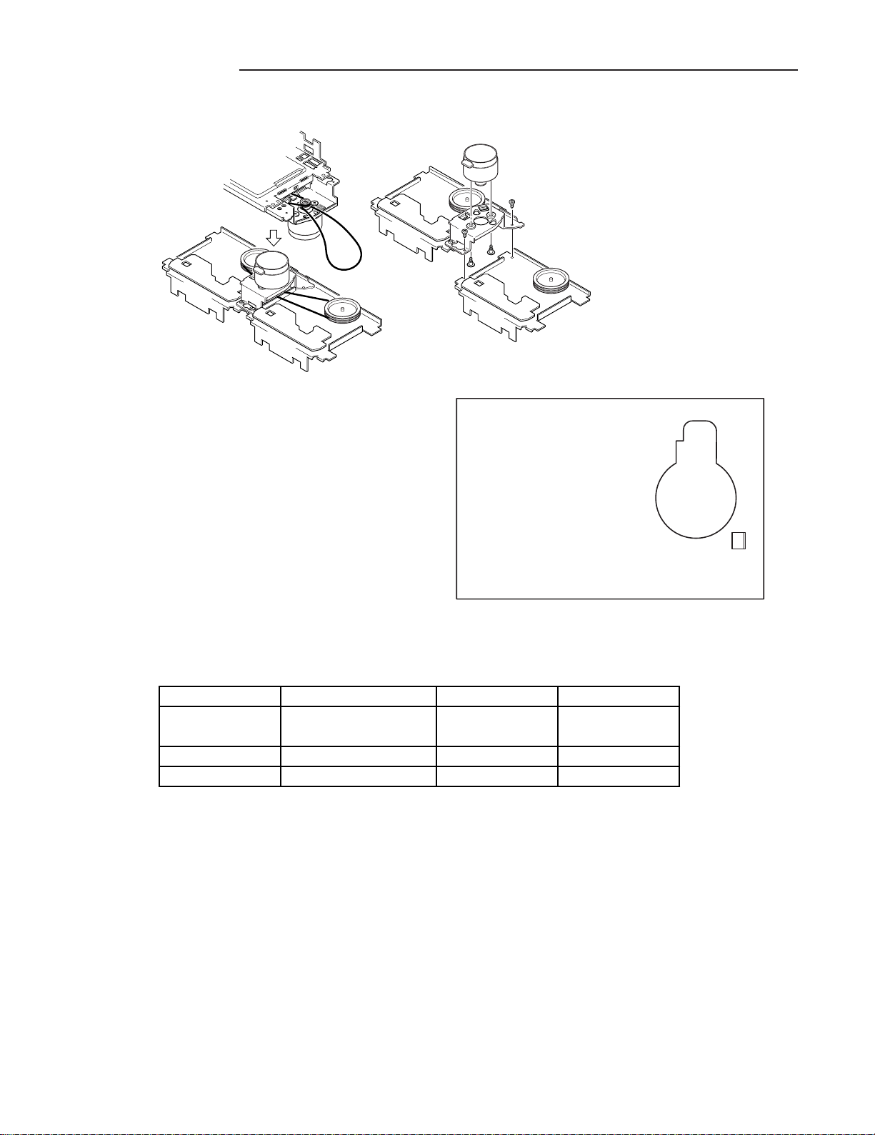
EXPLODED VIEW (TAPE MECHANISM)
TM05
TM08
TM06
TM03
TM02
TM01
TM03
TM04
TM07
TAPE MECHANISM (TM-C50PRMEC-SH
. . . Only Initial)
REF.NO. PART NO. DESCRIPTION
614 303 0225 ASSY,MECHA,TM-C50PRMEC-SH
TM01 614 293 6634 HEAD,R/P
TM02 645 033 3354 HEAD,ERASE
TM03 645 028 0030 ASSY,PINCH-ARM
TM04 645 025 5892 MAIN-BELT
TM05 645 029 6246 MAIN-BELT
TM06 614 293 9505 ASSY,MOTOR,PLAY MECHA MOTOR
TM07 645 028 0542 ASSY,PINCH-ARM
TM08 645 036 3726 HEAD,PLAY,AUDIO
- 15 -
Page 18

EXPLODED VIEW (CD CHANGER MECHANISM)
CM61
CM61
CM03
CM19
CM23
CM19
CM61
CM14
CM11
CM52
CM61
CM62
CM02
CM63
CM18
CM19
CM17
CM10
CM67
CM62
3
CM62
CM12
CM13
CM63
CM07
1
2
CM62
A
CM08
CM19
CM04
CM65
CM32
CM34
CM25
CM29
CM45
CM60
CM47
CM39
CM40
CM36
CM66
CM66
CM49
CM38
CM35
CM46
CM44
CM60
CM31
CM30
CM48
CM37
CM51
CM43
CM50
CM33
CM41
CM43
CM50
CM06
CM09
B
CM64
CM65
CM65
CM64
CD BASE
MECHANISM
CM01
CM65
CM16
CM15
CM27
CM28
CM24
B
A
CM26
CM61
CM05
CM61
- 16 -
Page 19

PARTS LIST
CD MECHANISM
(PM-CDS800TP-SH ... Only Initial)
REF.NO. PART NO. DESCRIPTION
CM01 645 033 6072 ASSY,CHASSIS,CHASSIS ASSY
CM02 645 033 7512 DRAWER 2
CM03 645 033 5976 ASSY,HOLDER L,
DRAWER HOLDER L ASS
CM04 645 033 6898 ASSY,HOLDER R3B,
DRAWER HOLDER R ASSY
CM05 645 033 6041 ASSY,PC BOARD A
CM06 645 033 6065 ASSY,PC BOARD B
CM07 645 033 6058 ASSY,PC BOARD C
CM08 645 033 5945 LEAD WIRE
CM09 645 033 5952 LEAD WIRE
CM10 645 033 6713 SPACER SW
CM11 645 033 6027 ASSY,GEAR DRIVE,
SINCHRO GEAR ASSY
CM12 645 041 2417 ASSY,CRG 101,CARRIAGE NO.1
CM13 645 041 2424 ASSY,CRG 201
CM14 645 041 2431 ASSY,CRG 301
CM15 645 033 5877 INSULATER
CM16 645 033 5884 INSULATER
CM17 645 033 5907 CUSHION
CM18 645 033 6324 BEVEL GEAR 4
CM19 645 033 5990 ASSY,GEAR STAR,
CARRIAGE LIFT GEAR
CM23 645 033 6089 COVER 2
CM24 645 033 6539 SHAFT
CM25 645 033 6461 SLIDER 4
CM26 645 033 6201 GEAR SPLINE
CM27 645 033 6232 BEVEL GEAR 1
CM28 645 033 6270 GEAR IDLER 1
CM29 645 033 6102 PLATE SPRING
CM30 645 033 6287 BEVEL GEAR 3
CM31 645 033 6225 PULLEY C
CM32 645 041 2448 ASSY,CLAMPER SA,CLAMPER
(SANYO)
REF.NO. PART NO. DESCRIPTION
CM33 645 033 6140 ARM SLIDER R
CM34 645 033 6157 ARM SLIDER L
CM35 645 033 6430 SLIDER 1
CM36 645 033 5969 ASSY,SLIDER 2,
FWD/RVS SLIDE ASSY
CM37 645 033 6980 ARM STOPPER A2
CM38 645 033 6416 ARM STOPPER B
CM39 645 033 6263 GEAR IDLER A2
CM40 645 033 6218 GEAR IDLER C
CM41 645 033 6447 LEVER
CM43 645 033 6454 LIFTER,CARRIGE LIFT UP
CM44 645 033 5778 BELT
CM45 645 033 5785 BELT
CM46 645 033 7048 SPRING
CM47 645 033 6393 PULLEY A
CM48 645 033 6003 ASSY,MOTOR CRG S,
CARRIGE MOTOR ASSY
CM49 645 033 6010 ASSY,MOTOR DRW S,
DRAWER MOTOR ASSY
CM50 645 033 5723 SPRING
CM51 614 303 7545 SPRING
CM52 645 033 5747 SPRING
CM60 645 033 5648 WASHER
CM61 645 033 5594 SCREW
CM62 645 033 7031 SCREW
EXPLODED VIEW (CD BASE MECHANISM)
PM09
PM02
PM09
PM08
PM07
PM06
PM03
PM08
PM04
PM05
PM01
PM10
CD BASE MECHANISM (CDDA11-SASH...Only Initial)
REF.NO. PART NO. DESCRIPTION
PM01 620 021 8436 PLUG 6P
PM02 620 233 0853 ASSY MOTOR
PM03 620 236 3776 COVER,GEAR
PM04 620 230 8753 GEAR, MIDDLE
PM05 620 230 8760 GEAR,DRIVE
PM06 620 231 0596 SHAFT SLIDE
PM07 620 233 0860 SWITCH LEAF
PM08 411 104 8401 SCR PAN PCS 2X3
PM09 411 027 5402 SCR S-TPG FLT 2.6X6
PM10 620 236 0836 PWB,MOTOR
- 17 -
Page 20

IC BLOCK DIAGRAM & DESCRIPTION
IC101 LA9241ML (Servo Signal Processor)
No. Pin Name I/O Function
1 FIN2 I Connection Pin for Photo Diode of Pickup.
2 FIN1 I FIN2 + FIN1 = RF, FIN2 - FIN1 = FE
3 E I Connection Pin for Photo Diode of Pickup.
4 F I E - F = TE
5 TB I Input Pin for DC ingredient of TE Signal.
6 TE- I Connection Pin for Gain Setting Resistor of TE
Signal to TE Signal Pin.
7 TE O Output Pin for Tracking Error Signal.
8 TESI I Input Pin for Track Error Sense Comparator.
TE Signal through Band Pass, and Inputted.
9 SCI I Input Pin for Shock Detection.
10 TH I Connection Pin for Time Constant Setting of
Tracking Gain.
11 TA O Output Pin for TA Amplifier.
12 TD- I Connection Pin for Constant Tracking Phase
Compensation, Consist of between TD and VR.
13 TD I Connection Pin for Constant of Tracking Phase
Compensation.
14 JP I Connection Pin for Amplitude Setting of Tracking
Jump (Kick Pulse) Signal.
15 TO O Output Pin for Tracking Control Signal.
16 FD O Output Pin for Focusing Control Signal.
17 FD- I Connection Pin for Constant of Focusing Phase
Compensation, Consist of between FD and FA.
18 FA+ I Connection Pin for Constant of Focusing Phase
Compensation, Consist of between FD- and FA-.
19 FA- I Connection Pin for Constant of Focusing Phase
Compensation, Consist of between FA and FE.
20 FE O Output Pin for Focusing Error Signal.
21 FE- I Connection Pin for Gain Setting Resistor of FE
Signal to FE Signal Pin.
22 AGND - Ground for Analog Signal.
23 SP O Output Pin for Single End of Input Signal of the
CV+, CV- Pin.
24 SPI I Input Pin for Spindle Amplifier.
25 SPG I Connection Pin for Gain Setting Resistor, when
Spindle 12 cm Mode.
26 SP- I Connection Pin for Constant of Spindle Phase
Compensation with SPD Pin.
27 SPD O Output Pin for Spindle Control Signal.
28 SLEQ I Connection Pin for Constant of Sled Phase
Compensation.
29 SLD O Output Pin for Sled Control Signal.
30 SL- I Input Pin for Sled Signal from Micro Processor.
31 SL+ I
32 JP- I Input Pin for Tracking Jump Signal from Digital
33 JP+ I Signal Processor.
No. Pin Name I/O Function
34 TGL I Input Pin for Tracking Gain Control Signal from
Digital Signal Processor. TGL = H : Gain Low
35 TOFF I Input Pin for Tracking Off Control Signal from Digital
Signal Processor. TOFF = H : OFF
36 TES O Output Pin for Track Error Sense Signal to Digital
Signal Processor.
37 HFL I High Frequency Level Signal Use Detection
Main-Beam Position is on the pit or mirror.
38 SLOF I Input Pin for Sled Servo Off Control.
39 CV- I Input Pin for Constant Linear Velocity Error
40 CV+ I Signal from Digital Signal Processor.
41 RFSM O Output Pin for RF Signal.
42 RFS- I Connection Pin for Gain Setting of RF and
Constant Setting of 3T Compensation of the
EFM Signal with RFSM Pin.
43 SLC O Slice Level Control Signal is Output Pin.
It Control Level of Data-Slice by Digital Signal
Processor of the RF Waveform.
44 SLI I Input Pin for Level Control of Data-Slice by
Digital Signal Processor.
45 DGND - Ground for Digital Signal.
46 FSC O Output Pin for Focus Search Smooth Condenser
47 TBC O Connection Pin for Variable Range Setting of
EF Balance.
48 NC - No Connect
49 DEF O Output Pin for Defect Detection of Disc.
50 CLK I Input Pin for Reference Clock Pulse.
(4.23 MHz of Digital Signal Processor)
51 CL I Input Pin of Clock Pulse for Command from
Micro Processor.
52 DAT I Input Pin of Data for Command from Micro
Processor.
53 CE I Input Pin of Chip Enable for Command from Micro
Processor.
54 DRF O Output Pin for Detect of RF Level.
55 FSS I Select Pin for Focus Search Mode
56 VCC2 - VCC for Servo and Digital Root.
57 REFI I Bus Control Connection Pin for Reference Voltage.
58 VR O Output Pin for Reference Voltage.
59 LF2 I Connection Pin for Time Constant Setting of
Detect Detection of the Disc.
60 PH1 I Capacitor Connection Pin for Peak-hold of RF Signal.
61 BH1 I Capacitor Connection Pin for Bottom-hold of
RF Signal.
62 LDD O Output Pin of APC (Automatic Power Control) Circuit.
63 LDS I Input Pin of APC (Automatic Power Control) Circuit.
64 VCC1 I VCC for RF Root.
- 18 -
Page 21

IC BLOCK DIAGRAM & DESCRIPTION
IC102 LC78622NE (Digital Signal Processor)
No. Pin Name I/O Function
1 DEFI I Input terminal for detect signal of defect
2 TAI I Input terminal for test.
3 PDO O The phase comparison output terminal for
external VCO control.
4 VVSS - Ground terminal for built-in VCO
5 ISET I Resistance connection terminal for
electric current adjustment of PDO output.
6 VVDD - Built-in VCO power supply terminal.
7 FR I VCO frequency range adjustment.
8 VSS - Ground for Digital
9 EFMO O EFM signal output terminal for slice level control.
10 EFMIN I EFM signal input terminal for slice level control.
11 TEST2 I TEST pin. Normal time is non connection.
12 CLV+ O Output terminal for Disc motor control.
13 CLV- O Output terminal for Disc motor control.
14 V/P O Change of rough servo / phase control
Rough servo : "H", Phase control : "L"
15 HFL I Input terminal of track search signal.
16 T ES I Input terminal of tracking error signal.
17 TOFF O Output terminal of tracking off.
18 TG L O Output terminal for change of tracking gain.
19 JP+ O Output terminal for tracking jump control.
20 JP- O Output terminal for tracking jump control.
21 PCK O Clock monitor output terminal for EFM data
playback. (4.3218 MHz)
22 FSEQ O Output terminal for detect of SYNC signal.
23 DVDD - +5V
24 CONT1 I/O
25 CONT2 I/O This output can control at serial control from
26 CONT3 I/O micro processor.
27 CONT4 I/O
28 CONT5 I/O
29 EMPH O Output terminal of de-emphasis monitor .
"H" : de-emphasis
30 C2F O Output terminal of C2 flag
31 DOUT O Output terminal of digital out
DEFI
EFMIN
EFMO VVDDVVSSPDO ISET FR PCK TAI
9
1
Slice level
10
Control
4
6
VCO Clock Oscillator
& Clock Control
357 2
No. Pin Name I/O Function
32 TEST3 I Test pin.
33 TEST4 I Test pin.
34 NC - Non connection.
35 MU TEL O Mute output terminal for L-ch
36 LVDD - Power supply for L-ch
37 LCHO O Output terminal for L-ch
38 LVSS - GND for L-ch
39 RVSS - GND for R-ch
40 RCHO O Output terminal for R-ch
41 RVDD - Power supply for R-ch
42 MUTER O Mute output terminal for R-ch
43 XVDD - Power supply of crystal oscillation
44 XOUT O Connection terminal of crystal oscillation (16.9344MHz)
45 XIN I Connection terminal of crystal oscillation (16.9344MHz)
46 XVSS - GND of crystal oscillation
47 SBSY O Output terminal for synchronizing signal of
sub-cord block
48 EFLG O Output terminal for correction monitor of C1, C2,
Single and Double
49 PW O Output terminal for sub-cord of P, Q, R, S, T, U and W
50 SFSY O Output terminal for synchronizing signal of
sub-cord frame
51 SBCK I Input terminal for readout clock of sub-cord
52 FSX O Output terminal of Synchronizing signal (7.35kHz)
53 WRQ O Output terminal for standby of sub-cord Q output
54 RWC I Input terminal of read / write control
55 SQOUT O Out put t ermi nal o f sub-cord Q
56 COIN I Input terminal of command from micro processor
57 CQCK I Clock input for reading sub-cord from SQOUT
58 RES I Reset (turn on : L)
59 TST11 O Test pin
60 16M O 16.9344MHz
61 4.2M O 4.2336MHz
62 TEST5 I Test pin
63 CS I Chip select terminal
64 TEST1 I Test pin
TEST2 TEST4
21
TST11
TEST1 TEST3 TEST5
59 64 11 32 33 62
2K ~8bit
RAM
VDDV
23
SS
8
RAM Address
Generatorl
FSEQ
CLV+
CLV-
SBCK
SBSY
SFSY
WRQ
SQOUT
CQCK
COIN
RWC
Syncrnous Detect
22
EFM Demodulation
12
13
14
V/P
PW
49
51
47
50
63
CS
53
55
57
56
54
CLV
Digital Servo
Subcode Dxract
QCRC
µCOM
Inter Fase
TGL
General Ports
CONT3
CONT1
CONT2
CONT4
Servo Commander
15 16 17 20 19 58 18 24 25 26 27 28 29 48 60 61 46 52 45 44 43 39 41 42 40 37 35 38 36
RESJP+JP-TOFFTESHFL
C1 C2 Error Detect &
Correct Control Flag
X'tal Root
Timing Generator
4.2M16MEFLGEMPHCONT5
XV
SS
XV
DD
XINFSX
XOUT
Interpolalation Mute
Quadruple Over Sampling
RV
DD
RV
SS
MUTER
- 19 -
Billingual
Digital Attenuator
Digital Filter
1bit DAC
L.P.F
RCHO
C2F
30
Digital Out
LV
DD
MUTELLCHO
LV
SS
31
DOUT
(NC)
34
Page 22

g
2
8
6
7
3
5
1
9
Vcc
Vref
Vs
OUT1
OUT2
GND
IN1
IN2
Protective Circuit
(Heat Interception)
REG
IC BLOCK DIAGRAM & DESCRIPTION
1
2
3
4 5 6 7 8
16
1514131211
10
9
VSS
DATA
CLOCK
Q0Q1Q2
Q3
Q5Q6Q7Q8Q9
Q10
VDD
CONTROL
CURCUIT
Q11
Q4
12 BIT SHIFT
RESISTOR
LATCH
OUTPUT BUFFER (OPEN DLAIN)
IC103 LA6541 (Pickup Actuator & CD Mechanism Motor)
Vcc Vref VIN4 VG4 Vo8 Vo7 GND Vo6 Vo5 VG3 VIN3 CD RES
11k
Vcc
11k
IC131, IC132 TA7291S (Bridge Driver)
131415161718192021222324
Level
Sift
Level
Sift
123456 789
Vcc Mute VIN1 VG1 Vo1 Vo2 GND Vo3 Vo4 VG2 VIN2 Re
BTL
Driver
BTL
Driver
BTL
Driver
BTL
Driver
IC211 TA8176SN (FM Front End)
RF OUT
MIX IN
MIX OUT
AGC
BY-PASS
RF IN
IF OUT
5
7
Vcc
1
2
3
Vcc
MIXER
AGC DET
9 4 6 10
8
IF
Buffer
Amp
BIAS
Vcc
Buffer
Buffer
GND
FM/TV SW
Local
11
12
Level
Sift
Level
Sift
11k11k
10 11 12
RESET
Regulator
OUT Reg IN
IC231 LA1832ML (AM / FM IF Amplifier & FM-MPX)
AGC
COMP
TUNING
DRIVE
18
6
DET
7
MUTE
16
REG
FF FF FF
VCO
AM
/FM
SW
12
OSC
OSC
BUFFER
OUT
23
ALC
AM
OSC
BUFF
4
24
LEVEL
DET
22
FM
IF
S-CURVE
FM
DET
1
2
AM
AM
RF
MIX
AMP
AM/FM
IF BUFF
8
10
21 20 19
AMIFAM
AM
FM
3
GND
STEREO
DRIVE
PHASE DET
5
11
9
VCC
STEREO
SW
TRIG
PILOT
DET
DECODER
15 14
17
13
IC245 LC72121M (PLL Synthesizer)
2
Vssx
XIN
XOUT
FMIN
AMIN
V
Vssd
1
24
17
16
CE
3
DI
4
CL
5
6
DO
DD
18
15
1/2
CCB
I / F
POWER
ON
RESET
REFERENCE
DIVIDER
SWALLOW COUNTER
1/16, 1/17 4bits
12bits PROGRAMMABLE
DIVIDER
DATA SHIFT REGISTER LATCH
8910 11
7
BO2 BO3 BO4
BO1
IC362 TC4011BF (NAND Gate)
VDD A4
14
1
B4 X4 X3 B3 A3
12
13
3
2
X1 X2A1 B1 B2 A2 VSS
IC361 BU2090F (12bit Serial Parallel Converter)
19
20
21
22
13
PD
AIN
AOUT
Vssa
IFIN
No.
Pin Name Port Name
Function
1 VSS VSS Ground
2 DATA D-OUT Data input
3 CLOCK EX1-CLK Clock input
4 Q 0 BEAT Tape beat chancel output (L=Pos1, H=Pos.2)
5 Q 1 OSC Tape oscillation circuit control (L=OFF, H=ON)
6 Q 2 Not used
7 Q 3 R-MUTE Tape REC mute output (L=OFF, H=ON)
8 Q 4 DECK-A/B Deck A / B control (L=B, H=A)
9 Q 5 Not used
10 Q6 R/P Tape Rec / Play control (L=Rec, H=Play)
11 Q7 Not used
12 Q8 MOTOR Tape motor output (H=OFF,L=ON)
13 Q9 A-PLY-PL Dack A Play Plunger output (H=OFF,L=ON)
14 Q1 0 B-PLY-PL Dack B Play Plunger output (H=OFF,L=ON)
15 Q1 1 Not used
16 VDD VDD Power supply
- 20 -
PHASE DETECTOR
CHARGE PUMP
UNLOCK
DETECTOR
UNIVERSAL
COUNTER
14
IO2
IO1
11
4
5
8910
6
7
Page 23

IC BLOCK DIAGRAM & DESCRIPTION
IC363 BA7755A (Head Switch)
IC371 TA8189N (Pre-Amplifier for Tape Deck)
1
VCC
HEAD
SWITCH
GND
CTRL2
52 3
4
CTRL1
IC425 NJM7805FA (3-Terminal Voltage Regulator)
IC458 LC75342M (Electronically controllable
electronic volume)
CL
VDD
VREFNCROUT
RBASS2
RBASS1
RTRE
RIN
LBASS1
LTRE
LIN
RSEL0R4R3R2R1
L4L3L2
LSEL0
30 29 28 27 26 25 24 23 222120
123456789101112131415
DI
CE
VSS
TEST
LOUT
LBASS2
19 18 17 16
L1
NC
NC
IC604, IC605 BU2090F (12bit Serial Parallel Converter)
VSS
VDD
1
16
DATA
CLOCK
2
3
CONTROL
CURCUIT
OUTPUT BUFFER (OPEN DLAIN)
12 BIT SHIFT
RESISTOR
LATCH
IC413 LA2615M (Surround)
GDR GUR ACG LPFC LED VCC L-OUT R-OUT
16 15 14 13 12 11 10 9
ANALOG
SURROUND
VREF
On/Off H/L H/L GND HPFC VREF L-IN R-IN
IC602 NJM4558M (Operation Amplifier)
A OUTPUT
A -INPUT
A +INPUT
1
A
2
B
3
8
7
6
VCC(+)
B OUTPUT
B -INPUT
87654321
4 5 6 7 8
Q0Q1Q2
Q3
9
10
Q4
Q5Q6Q7Q8Q9
Q10
VEE(-)
4
1514131211
Q11
5
B +INPUT
IC604 BU2090F (12bit Serial Parallel Converter) IC605 BU2090F (12bit Serial Parallel Converter)
No.
No.
Pin Name Port Name
Function
1 VSS VSS Ground
2 DATA D-OUT Da ta input
3 CLOCK EX2_CLK Clock input
4 Q 0 Not used
5 Q 1 SUR_3 Output for Surround LSI control
6 Q 2 SUR_2 Output for Surround LSI control
7 Q 3 SUR_1 Output for Surround LSI control
8 Q 4 LED_0 Not used
9 Q 5 LED_1 DISC_3 LED OUTPUT (L=ON)
10 Q6 LED_2 CD STOP KEY LED OUTPUT (L=ON)
11 Q7 LED_3 FWD KEY LED OUTPUT (L=ON)
12 Q8 LED_4 CD PLAY KEY LED OUTPUT (L=ON)
13 Q9 LED_5 DISC_1 LED OUTPUT (L=ON)
14 Q10 LED_6 BACK KEY LED OUTPOUT (L=ON)
15 Q11 LED_7 DISC_2 LED OUTPUT (L=ON)
16 VDD VDD Power supply
Pin Name Port Name
1 VSS VSS Ground
2 DATA D_OUT Data input
3 CLOCK EX3_CLK Clock input
4 Q 0 S20 FL-S20 control
5 Q 1 LED_8 PASS_HI LED OUTPUT (L=ON)
6 Q 2 LED_9 PASS_MID LED OUTPUT (L=ON)
7 Q3 LED_10 PASS_LOW LED OUTPUT (L=ON)
8 Q4 LED_11 SOUND JAZZ LED OUTPUT (L=ON)
9 Q5 LED_12 SOUND ROCK
10 Q6 LED_13 SOUND POP LED OUTPUT (L=ON)
11 Q7 LED_14 SOUND CLASSIC LED OUTPUT (L=ON)
12 Q8 LED_15 SOUND LED OUTPUT (L=ON)
13 Q9 LED_16 BASS_HI LED OUTPUT (L=ON)
14 Q 1 0 LED_17 BASS_MID LED OUTPUT (L=ON)
15 Q 1 1 LED_18 BASS_LOW LED OUTPUT (L=ON)
16 VDD VDD Power supply
- 21 -
Function
Page 24

IC BLOCK DIAGRAM & DESCRIPTION
(ON=Low)
IC601 LC866548A (Micro Processor)
No. Name I/O Function
1 JOG+ I Input JogDial
2 JOG- I Input JogDial
3 D_CLK O Serial clock output for Tu/Vol_Func IC
4 D_OUT O
5 EXI_CLK O Serial clock output for extend IC1(DECK)
6 EX2_CLK O Serial clock output for extend IC2(LED)
7 EX3_CLK O Serial clock output for extend IC3(LED)
8 VF_CE O Serial latch output for Vol_Func IC
9 TU_CE O Serial latch output for Tuner IC
10 TU_DI I Serial date output for Tuner IC
11 O Not used
12 RESET I Reset terminal
13 XT1 I Sub clock connection terminal
14 XT2 O Sub clock connection terminal
15 VSS Ground
16 CF1 I Main clock connection terminal (6MHz)
17 CF2 O Main clock connection terminal (6MHz)
18 VDD Power supply (+5V)
19 KEY0 I Key input
20 KEY1 I Key input
21 KEY2 I Key input
22 CD_SW0 I SW input SW2(EXTRA) SW3(HOME)
23 CD_SW1 I SW input SW4(C_No.) SW5(C_No.)
24 CD_SW2 I SW input SW7(Fwd) SW8(Revs)
25 CD_SW3 I SW input SW6(Open) Pick Limit switch
26 LEVEL I LEVEL input
27 WRQ I CD DSP interface (sub Q Request)
28 PROTECTOR I Set protecto r (Irregular:Low)
29 IR I Remote control input
30 Digit13 O FL digit output
31 Digit12 O FL digit output
32 Digit11 O FL digit output
33 Digit16 O FL digit output
34 Digit10 O FL digit output
35 Digitl9 O FL digit output
36 Digit15 O FL digit output
37 Digit8 O FL digit output
38 Digit7 O FL digit output
39 Digit14 O FL digit output
40 Digit6 O FL digit output
41 Digit5 O FL digit output
42 Digit 4 O FL digit output
43 Digit3 O FL digit output
44 Digit2 O FL digit output
45 Digit1 O FL digit output
46 VDD Power supply (+5V)
47 Seg19 O FL Segment output
48 Seg18 O FL Segment output
49 Seg17 O FL Segment output
50 Seg16 O FL Segment output
51 VP FL drive output power
Serial date output for Tu/Vol_Func/extend IC
No. Name I/O Function
52 Seg1 O FL Segment output
53 Seg2 O FL Segment output
54 Seg3 O FL Segment output
55 Seg4 O FL Segment output
56 Seg5 O FL Segment output
57 Seg6 O FL Segment output
58 Seg7 O FL Segment output
59 Seg15 O FL Segment output
60 Seg14 O FL Segment output
61 Seg13 O FL Segment output
62 Seg12 O FL Segment output
63 Seg11 O FL Segment output
64 Seg10 O FL Segment output
65 Seg9 O FL Segment output
66 Seg8 O FL Segment output
67 SEL_RVS_A I
68 SEL_POW_RY I Power relay select (ON = high)
69 SEL_12_24 I Timer display (24h=High 12h=Low)
70 V_CHK I
71 C2F I C2Flag (DSP)
72 VDD Power supply (+5V)
73 G_REVS I
74 G_FWD I
75 B_PACK I
76 B_PALY I Play(B side) switch (ON=Low)
77 A_PACK I Tape set detection(A side) switch (ON=Low)
78 A_PLAY I Play(A side) switch (ON=Low)
79 A_REEL I Reel turn signal(A side)
80 B_REEL I Reel turn signal(B side)
81 POW_RY O Power relay control output (ON=High)
82 P_CON O Power control signal (Power on=high)
83 SP_RY O speaker relay control output
84 PRE_MUTE O PRE MUTE output (Mute on = High)
85 MAIN_MUTE O Main mute output (Mute on=High)
86 PULL_UP O pull-up power output (ON=Low)
87 DSP_RESET O Reset signal to DSP (CD)
88 CLK_SHIFT O Main clock shift
89 VSS Ground
90 VDD Power supply (+5V)
91 CARRIAGE+ O CARRIAGE-MOTOR control output+
92 CARRIAGE- O CARRIAGE-MOTOR control output93 DRAWER+ O DRAWER control output+
94 DRAWER- O DRAWER control output95 COIN O CD_DSP interface (command data output)
96 SQOUT I CD_DSP interface (SubQ data input)
97 CQCK O CD_DSP interface (clock)
98 VD_GND O GND control output for micon power check
99 DRF I DRF signal input
100 RWC O CD_DSP interface (command latch)
Tape Mechanism select
(Reverse=High, Normal =Low)
Power suspension detection
Power suspention = Low/Micon power
hk D
Failure record switch (Tape B side)
Failure record switch (Tape A side)
Tape set detection(B side) switch (ON=Low)
WN=L
=
- 22 -
Page 25

IC & TRANSISTOR VOLTAGES
IC101 LA9241M
Pin No. 123456789101112131415
PLAY 2 .5 2.5 2.5 2.5 2.5 2.5 2.5 2.5 2.5 2.5 2.5 2. 5 2.5 2.5 2.6
STOP 2.5 2.5 2.5 2.5 2.5 2. 5 2.5 2.5 2.5 2.5 2.5 2.5 2.5 2.5 2.5
Pin No. 16 17 18 19 20 21 22 23 24 25 2 6 27 28 29 30
PLAY 2 .8 2.5 2.5 2.5 2.6 2.5 0 2 . 4 2.4 2. 5 2.5 2.8 2. 5 2.7 2.3
STOP 2.5 2.5 2.5 2.5 2.5 2. 5 0 2.5 2.5 2.5 2.5 2.5 2.5 2.5 2. 3
Pin No. 31 32 33 34 35 36 37 38 39 40 4 1 42 43 44 45
PLAY 2 .3 0 0 4 .9 0 1. 5 0 0 0 0 .8 2.4 2.4 2.5 2.5 0
STOP 2.3 0 0 4.9 5. 0 4.8 0 4.9 0 0 1.6 2.4 2.4 2.5 0
Pin No. 46 47 48 49 50 51 52 53 54 55 5 6 57 58 59 60
PLAY 2 .5 2.5 0 0 2.3 4.5 0 0 4.9 0 5 . 0 2.5 2. 5 2.5 2.6
STOP 2.5 2.5 0 0 2.3 4.8 4.8 0 0 0 5.0 2.5 2.5 0.9 0.9
Pin No. 61 62 63 64
PLAY 2 .3 3.9 0 5. 0
STOP 2.2 4.3 0 5 .0
(V)
IC102 LC78622N
Pin No. 123456789101112131415
PLAY 0 0 1.6 0 1. 6 5. 0 0.3 0 2.5 2.5 0 0 . 9 0 0 0
STOP 00001.65.0002.52.40004.90
Pin No. 16 17 18 19 20 21 22 23 24 25 2 6 27 28 29 30
PLAY 1 .7 0 5.0 0 0 2. 4 5.0 5. 0 4.9 1.5 0 0 1. 8 0 0
STOP 4.9 4.9 4.9 0 0 2 .4 0 4.9 4. 8 2.4 0 0 2. 4 0 4.9
Pin No. 31 32 33 34 35 36 37 38 39 40 4 1 42 43 44 45
PLAY 2 .4 00005.22.1002.15.205.02.02.0
STOP 2.4 0 0 0 4.9 5.2 2.1 0 0 2.1 5. 2 4.9 4.9 2.0 2.0
Pin No. 46 47 48 49 50 51 52 53 54 55 5 6 57 58 59 60
PLAY 0 0. 1 0 0.1 0 0. 9 2. 5 0.9 0 0 0 4 .5 4.8 0 2. 2
STOP 0 0.1 2.2 0 2.5 1.3 2.5 0 0 0 4.8 4.8 4.8 0 2.1
Pin No. 61 62 63 64
PLAY 2 .2 0 0 0
STOP 2.2 0 0 0
IC103 LA6541
Pin No. 123456789101112131415
PLAY 8 .3 0 2.7 2. 5 4.1 3.5 3. 5 4.1 2.5 2. 7 5.0 7.7 5. 0 5.0 2.6
STOP 8.6 4.8 2.5 2.5 2.5 3. 9 3.8 4.0 2.5 2.5 5.0 7.8 5.0 5.0 2.5
Pin No. 16 17 18 19 20 21 22 23 24
PLAY 6 .3 3.8 3.9 3.8 3.9 2.5 2.5 2.5 8.4
STOP 2.5 3.9 3.9 3.9 3.8 2. 5 2.5 2.5 8.4
(V)
(V)
IC131 TA7291S
Pin No. 123456789
DR-OPEN 4.8 11.5 7. 4 0 0 11.0 0 .7 6.7 0
DR-CLOSE 0 11.5 0.7 0 0 11.0 7. 4 6. 7 4. 8
STOP 4.8 11.5 0.6 0 0 11.4 0.6 6.7 4.8
IC132 TA7291S
Pin No. 123456789
CA-OPEN 0 11.5 0.7 0 0 11.0 6 .3 5.6 4.8
CA-CLOSE 4.8 11.5 6.3 0 0 11.0 0. 7 5. 6 0
STOP 4.8 11.5 0.6 0 0 11.4 0.6 5.6 4.8
TRANSISTORS
PIN Q1301 Q1401
NAME B C E B C E
PLAY 4.5 1.9 3.9 8.2 5.0 5. 0
STOP 4. 9 1.6 4.3 8.3 5.0 7.7
- 23 -
(V)
(V)
Page 26

FL DISPLAY DESCRIPTION
S4
S1
S3
S6
S7
S11
S12S10
S13
S14
S15
S15
S15
S9
S8
S2
S5
G16G15G14G5G4G3G2
S11
S15
S12
G14 G15
S13
S14
S10
S11
S7
S8
S9
S5
S6
S2
S3
S5
S3
S4
S1
S15
S12
S9
S6
S3
S14
S11
S8
S5
S2
S13
S10
S7
S4
S1
S15
S12
S9
S6
S3
S14
S11
S8
S5
S2
S20
G10G9G8G7G1
S13
S10
S7
S4
S1
G11 G12 G13
S15
S14
S13
S12
S11
S10
S9
S8
S7
S6
S5
S4
S3
S2
S1
S16
S15
S19
S18
S17
S16
S15
S18
S17
S19
S15
S17
S16
S19
S18
G6
S5
- 24 -
Page 27

FL DISPLAY DESCRIPTION
TYPE : CK1951M
ANODE & GRID ASSIGNMENT
G1 G4
S1
S2
S3
S4
S5
S6
COMPU.
S7
LINE
S8
S9
S10
S11
S12
S13
S14
S15
S16
S17
S18
S19
S20
PIN ASSIGNMENT
Pin No.
Assignment
Pin No.
Assignment
F1, F2 : Filament G1~G16 : Grid S1~S20 : Anode NL : No Lead NP:No Pin
H : Always turned on Grid (Aplly Eh=35. OVdc (Typ.) all times)
D : Connect the lead pin of [D] to one of [F1] on the PCB.
G2
S1
S2
S3
S4
S5
S6
S7
S8
S9
S10
S11
S12
S13
S14
S15
S20
1 2 3 4 5 6 7 8 9 10 11 12 13 14 15 16 17 18 19 20 21 22 23 24 25 26 27
NL
(F1)
28 29 30 31 32 33 34 35 36 37 38 39 40 41 42 43 44 45 46 47 48 49 50 51 52 53
NL NL NL NL S1 S2 S3 S4 S5 S6 S14 S7 S8 S15 S9 S10 S16 S11 S12 S13 H NL NP F2
G3
S1
S2
S3
S4
S5
S6
S7
S8
S9
S10
S11
S12
S13
S14
S15
S20
NL
F1 NP NL D S8 S9 S10 S11 S12 S13 S14 S15 S7 S6 S5 S4 S3 S2 S1 S16 S17 S18 S19 NL S20
(F1)
S10
S11
S12
S13
S14
S15
S20
S1
S2
S3
S4
S5
S6
S7
S8
S9
G5
S1
S2
S3
S4
S5
S6
S7
S8
S9
S10
S11
S12
S13
S14
S15
S20
G6
A-
B
S3
S4
S5
S6
S7
S8
S9
S10
MPX
FADER
TIMER
ON
OFF
REC
SLEEP
+VOL-
G7
S1
S2
S3
S4
S5
S6
S7
S8
S9
S10
S11
S12
S13
S14
S15
TITLE
DISC
DTS
PBC
G8
S1
S2
S3
S4
S5
S6
S7
S8
S9
S10
S11
S12
S13
S14
S15
CHP
TRK
DOLBY
DIGITAL
G9
S1
S2
S3
S4
S5
S6
S7
S8
S9
S10
S11
S12
S13
S14
S15
KARAOKE
RANDOM
G10
S1
S2
S3
S4
S5
S6
S7
S8
S9
S10
S11
S12
S13
S14
S15
L
R
ST
CONDITION
G11
S1
S2
S3
S4
S5
S6
S7
S8
S9
S10
S11
S12
S13
S14
S15
MONO
LAST
G12
S1
S2
S3
S4
S5
S6
S7
S8
S9
S10
S11
S12
S13
S14
STEREO
MEMO
G13
S1
S2
S3
S4
S5
S6
S7
S8
S9
S10
S11
S12
S13
S14
1
ALL
CONT.
REPEAT
G14
S1
S2
S3
S4
S5
S6
S7
S8
S9
S10
S11
S12
S13
S14
S15
S16
S17
S18
S19
S20
G15
S1
S2
S3
S4
S5
S6
S7
S8
S9
S10
S11
S12
S13
S14
S15
S16
S17
S18
S19
S20
NL
(F2)
NL
(F2)
G16
S1
S2
S3
S4
S5
S6
S7
S8
S9
S10
S11
S12
S13
S14
S15
S16
S17
S18
S19
S20
153
- 25 -
Page 28

SCHEMATIC DIAGRAM (TUNER)
This is a basic schematic diagram.
- 27 -- 26 -
Page 29

SCHEMATIC DIAGRAM (AMPLIFIER)
This is a basic schematic diagram.
PRODUCT SAFETY NOTICE
Each precaution in this manual should be followed during servicing. Components identified with the IEC symbol
components in which safety can be of special significance. When replacing a component identified by
same ratings of resistance, wattage or voltage that are designated in the parts list in this manual. Leakage-current or resistance measurements must be made to determine
that exposed parts are acceptably insulated from the supply circuit before returning the product to the customer.
!!
!
in the parts list and the schematic diagram designated
!!
!
, use only the replacement parts designated, or parts with the
- 29 -- 28 -
Page 30

WIRING DIAGRAM (HEADPHONE, LED & REGULATOR)
HEADPHONE P.W.B LED P.W.B
REGULATOR P.W.B
- 33 -
Page 31

SCHEMATIC DIAGRAM (FRONT)
This is a basic schematic diagram.
- 35 -- 34 -
Page 32

SCHEMATIC DIAGRAM (CD)
This is a basic schematic diagram.
- 39 -- 38 -
Page 33

SCHEMATIC DIAGRAM (DECK)
This is a basic schematic diagram.
- 43 -- 42 -
Page 34

WIRING CONNECTION
CD CHANGER MECHANISM
LOARDING MOTOR
P.W.B
PICKUP
P.W.B
SPINDLE / SLED
MOTOR P.W.B
CN661
(2P)
STANDBY
LED
P.W.B
CN607
(2P)
CN602
(4P)
FRONT P.W.B
FL601
CN603
CN604
(12P)
(20P)
CN601
(22P)
CD P.W.B
CN115
(8P)
CN114
OPTICAL DIGITAL
OUT P.W.B
CN169
CN168
EXT. ANT
(3P)
FM 75 ohm
AM LOOP
ANTENNA
L-CH
SPEAKER
BOX
R-CH
SPEAKER
BOX
CN111
(15P)
(4P)
CN113
CN131
(3P)
CN123
(7P)
CN122
(20P)
JW101
CN201
ANT. IN
CN452
VIDEO/DVD IN
(AUDIO)
CN470
SPEAKERS OUT
(6 ohm MIN.)
JW3
(6P)
TUNER/AMP P.W.B
CN454
(10P)
CN412
(7P)
CN492
(7P)
CN455
(22P)
CN423
(4P)
CN491
(4P)
P.W.B
CN422
PHONES
CN432
(4P)
PHONES SCKET
BOARD TO BOARD
P.T SECONDARY
P.W.B
CN497
(3P)
CN495
(7P)
JW6
CN425
(3P)
REGULATOR
CN493
(4P)
P.W.B
CN335
BL
P.T
JW37 RE
JW38 BW
AC IN
CN336
BW
CN432
(4P)
CN337
RE
CN338
BW
SUB TRANS
P.W.B
FU499
T2A L 250V
P.T PRIMARY
P.W.B
CN373
(3P)
CN374
Jun. / '00 / 2000 BB Printed in Japan
CN313
(7P)
CN371
(3P)
CN372
(6P)
CN301
(10P)
CN312
(4P)
TAPE DECK
P.W.B
CN311
(6P)
CN302
(12P)
SENSOR
P.W.B
PLAY HEAD
TAPE DECK
MECHANISM
SENSOR
M
P.W.B
R/P HEADE HEAD
SANYO Technosound Co., Ltd.
Osaka, Japan
Page 35

WIRING DIAGRAM (TUNER & AMPLIFIER)
- 31 -- 30 -
Page 36

WIRING DIAGRAM (POWER TRANSFORMER)
POWER TRANSFORMER, PRIMARY P.W.B
POWER TRANSFORMER, SECONDARY P.W.B
- 32 -
Page 37

WIRING DIAGRAM (FRONT)
- 37 -- 36 -
Page 38

WIRING DIAGRAM (CD)
- 40 -
Page 39

WIRING DIAGRAM (DECK)
- 41 -
Page 40

WIRING DIAGRAM (DECK)
- 41 -
Page 41

WIRING DIAGRAM (OPTICAL DIGITAL OUT & SUB TRANS)
OPTICAL DIGITAL OUT P.W.B
SUB TRANS P.W.B
- 44 -
 Loading...