

Page 1
FILE NO.
Service Manual
REMOTE CONTROLLER RB-PT100RDS
CONTENTS
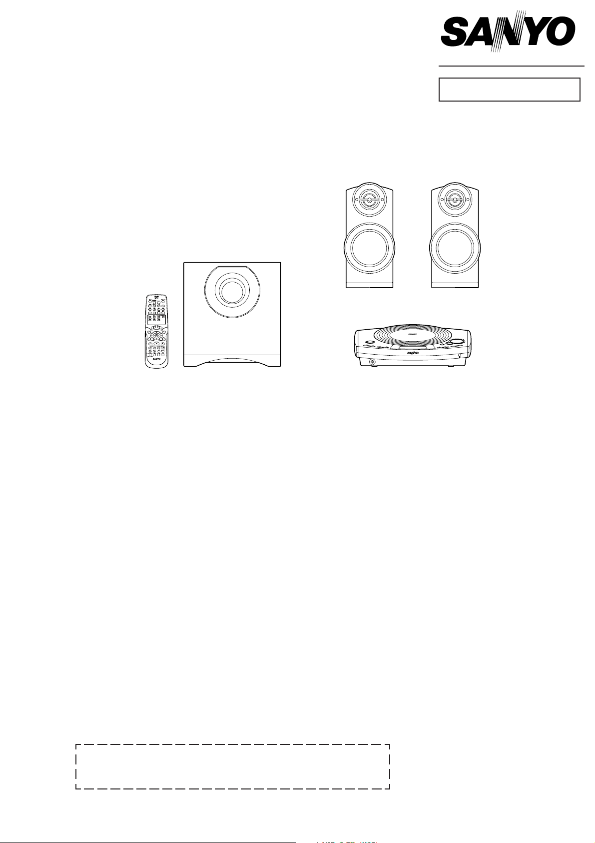
DVD Personal Theater System
T
U
N
I
N
G
P
R
E
S
E
T
P
H
O
N
E
S
DC-PT10
U
L
M
O
E
V
D
S
N
U
D
O
N
U
O
R
R
U
S
N
O
I
T
C
N
U
F
0 (XE)
PRODUCT CODE No.
129 675 01
Laser beam safety precaution .......................................... 1
DVD Mechanism Replacement ........................................ 1
Trouble shooting .............................................................. 2
Service mode ................................................................... 4
How to load software for MPEG P.W.Board .................... 7
Cautions for PWB or IC Assy exchange .......................... 7
Tuner adjustment ............................................................. 8
Tuner setup ...................................................................... 9
Exploded View (Cabinet & Chassis) ................................ 10
Parts List .......................................................................... 11
Exploded View & Parts List
(Sub woofer speaker) .......................................... 15
LCD Display ..................................................................... 17
IC Block Diagram & Description ....................................... 18
Block diagram .................................................................. 34
Wiring Connection ........................................................... 36
Schematic Diagram
(FRONT) ....................................................................... 37
(TUNER) ....................................................................... 40
(MAIN) Loder section .................................................... 44
MPEG section .................................................. 46
Preamplifier section .......................................... 48
(SPEAKER) .................................................................. 54
Wiring diagram
(LED) Parts Side View .................................................. 38
Pattern Side View ............................................... 38
(FRONT) ....................................................................... 38
(SWITCH) Parts Side View ........................................... 39
Pattern Side View........................................ 39
(TUNER) Parts Side View............................................. 42
Pattern Side View ......................................... 42
(MAIN) Parts Side View ................................................ 50
Pattern Side View ............................................. 52
(SPEAKER) Power Transformer .................................. 56
Main ......................................................... 56
Terminal ................................................... 56
This service manual consists of "JCX-PT100/XE" (Main unit : 129 674 01) ,
"ASX-PT100W/XE" (Sub Woofer Speaker : 165 082 01) and
"SX-PT100F/XE" (Front Speaker system : 165 083 01).
REFERENCE No.
SM5810566
Page 2
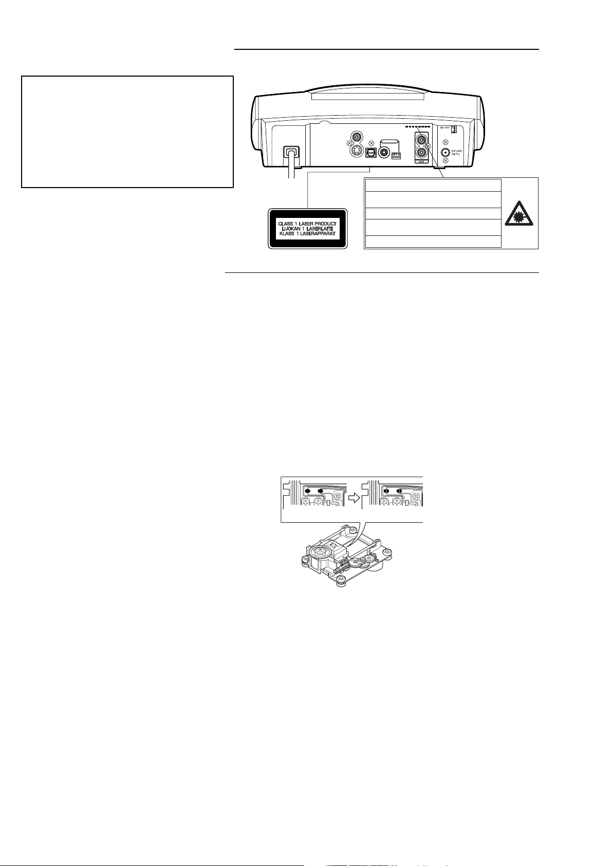
LASER BEAM SAFETY PRECAUTION
• Pick-up that emits a laser beam is used in this CD player section.
CAUTION :
USE OF CONTROLS OR ADJUSTMENTS
OR PERFORMANCE OF PROCEDURES
OTHER THAN THOSE SPECIFIED HEREIN
MAY RESULT IN HAZARDOUS RADIATION
EXPOSURE
LASER OUTPUT..........0.6 mW Max. (CW)
WAVELENGTH .............790 nm
DVD MECHANISM REPLACEMENT
VIDEO
OUT
TO SUBWOOFER
S-VIDEO
OPT.
CONTROL
AUDIO
OUT
DIGITALOUT
OUT
CAUTION – INVISIBLE LASER RADIATION WHEN OPEN AND
INTERLOCKS DEFEATED. AVOID EXPOSURE TO BEAM.
ADVARSEL – USYNLIG LASER STRÅLING VED ÅBNING, NÅR
SIKKERHEDSAFBRYDERE ER UDE AF FUNKTION, UNDGÅ UDS ÆTTELSE
FOR STRÅLING.
VARNING – OSYNLIG LASER STRÅLNING NÄR DENNA DEL ÄR ÖPPNAD
OCH SPÄRR ÄR URKOPPLAD. STRÅLEN ÄR FARLIG.
VORSICHT – UNSICHTBARE LASERSTRAHLUNG TRITT AUS, WENN
DECKEL GEÖFFNET UND WENN SICHERHEITSVERRIEGELUNG
ÜBERBRÜCKT IST. NICHT, DEM STRAHL AUSSETZEN.
VARO – AVATTAESSA JA SUOJALUKITUS OHITETTAESSA OLET ALTTIINA
NÄKYMÄTTÖMÄLLE LASERSÄTEILYLLE. ÄLÄ KATSO SÄTEESEEN.
1. Cautionary instructions in handling the assy
(Safety instructions)
Optical pickup
The laser beam used in the pickup is classified as "class 2".
Exposing your eyes or skin to the beam is harmful. Take care
not to do so.
(Caution against static electricity and leakage voltage)
Ground securely the work tables, tools, fixtures, soldering irons
(including those made of ceramic) and measuring instruments
used in the production lines and inspection departments that
handle loaders. The workers shall also be grounded.
(Cautionary instructions in handling)
Do not touch the object lens when handling a loader, or the lens
will be stained, resulting in inadequate playability.
There is no power supply protection circuit provided for this
product or adjustment/inspection device. Short-circuiting may
lead to fire or damage.
Take care so as to protect from exposure to water, the entry of
metallic pieces or dew condensation.
In particular, a strong magnet adjacent to the pickup will not only
get inoperative but can damage the pickup if a small metallic
piece, such as a screw or swarm, enters.
The loader edge can cause injury if inadvertently handled.
Do not touch a rotating disk, or injury may result.
This product is a precision device. Handle carefully.
A shock or dropping will cause misalignment or destruction. If it
should occur, refer to clause 2.
This product is so designed as to endure an initial shock
equivalent to a drop from a height of approx. 90 cm under the
packed condition.
After the initial shock, the resistivity will still remain at a level of
50 to 60 G, but the mechanical robustness will weaken.
Do not place in a dusty location.
The entry and deposition of dirt into or on the pickup lens or
moving section will cause malfunction or degradation.
(Connectors)
Do not connect or disconnect while power is on.
Connecting or disconnecting signal wires or the main power cord
when the power is on may destruct the unit or fixture.
When connecting, push all the way in securely.
An insufficient insertion may cause a bad contact, leading to an
erroneous operation.
Do not connect or disconnect roughly by an excessively strong
force, or a broken wire or bad contact may result.
Semiconductors are connected. Do not touch connector terminals
directly.
If the worker is grounded, there is nothing to worry about static
electricity, but the rust on the connector terminal surface caused
by the touch may result in bad contact.
(Caution)
Before disconnecting FFC
cable, make it "SHORT" as
shown left.
After connecting FFC
cable,make it "OPEN" as
shownleft.
(OPEN)(SHORT)
(Power source)
The power source need be good in quality (free from
instantaneous interruptions or noises).
A low quality power source may well cause malfunction.
(Storage)
Do not place or store in a dusty place or a place where dew
condensation is possible.
The entry and deposition of dirt or dust into or on the pickup lens
or moving section will cause malfunction or degradation.
Also, dew condensation causes rust; the rust penetrate into the
precision part of a pickup, causing malfunction, or degrading the
optical quality of the internal lens and reflector, which also leads
to malfunction.
- 1 -
Page 3
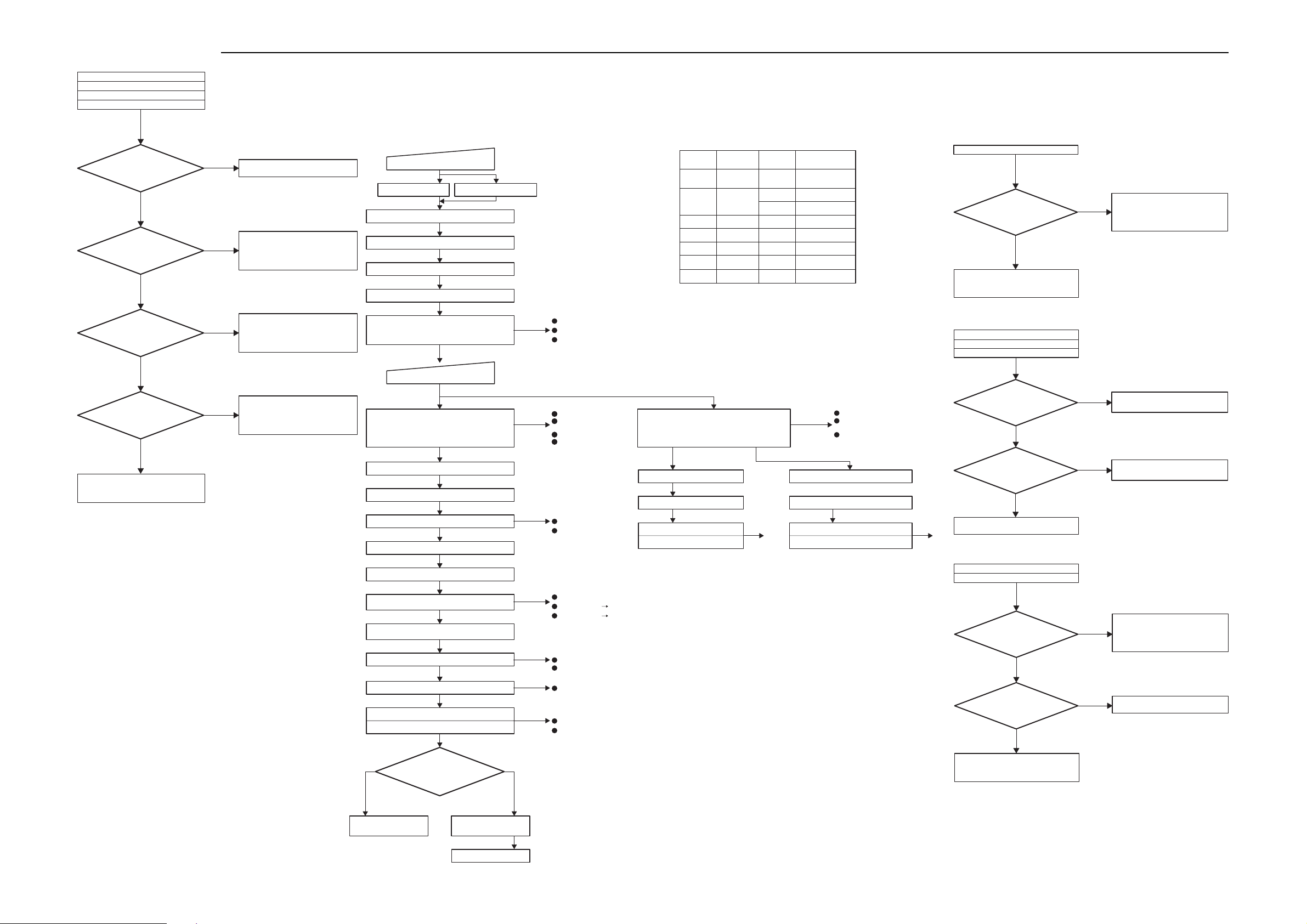
TROUBLE SHOOTING
VIDEO COMPOSITE OUT ; OK
TUNER OUTPUT ; OK
AUX OUTPUT ; OK
DVD/CD OUTPUT ; NG
LOADER CHANGE
OK?
N
3.3V,5V
CONFIRM
CN871 Pin5,6
Y
IC871 Pin7,8
CONFIRM
Y
IC800 AMCLK, ALRCLK,
AOUT0,ML,MC,MD1
CONFIRM
N
IC800 Pin
FLOATING CONFIRM
IC800 NG
Y
N
N
Y
LOADER CHANGE
5V LINE CONFIRM
3.3V LINE CONFIRM
IC493,494 PERIPHERAL
CIRCUIT CONFIRM
DAC IC871 PERIPHFRAL CONFIRM
DAC IC871 NG
MUTE CIRCUIT
IC881 PERIPHERAL CIRCUIT
DAC IC871 NG
CONFIRM
AC CORD PLUG
UK,XE,JP ONLY
5.6V,9V,±12V ; ON 5.6V,9V ; ON / ±12V ; OFF
IC470 RESET
X4700 CLOCK
IC470 ACTIVE
IC601 COMMUNICATION
POWER SUPPLY ; STANDBY mode
IC470 ACTIVE / P-CON ; LOW
DVD-PCON ; OFF
POWER KEY PRESS
DVD FUNCTION
P-COM ; HIGH
DVD-PCON ; HIGH
IC470 STANDBY DATA WAIT
±12V ; ON (UK,XE,JP)
IC480 COMMUNICATION
INITIALIZE ADAC (IC871)
RESET LOADER
READ,WRITE DATA IN EEPROM (IC801)
NG
IC470 VDD,RESET,OSC CONFIRM
IC470 COMMUNICATION CONFIRM
P-CON CONFIRM
FM,AM,AUX (VIDEO,TV)
NG
POWER KEY CONFIRM
IC601 COMMUNICATION
CONFIRM
±12V P-CON CONFIRM
DVD-P-CON CONFIRM
(IC493,IC494,IC495 etc)
NG
VDD,CLOCK CONFIRM
IC800 PERIPHERAL
CIRCUIT CONFIRM
IC470
X4700
IC480
IC481 SURROUND
IC601
IC871
IC801
IC493
P-COM ; HIGH /
DVD-PCON ; LOW
IC470 STANDBY DATA WAIT
±12V ; ON(UK,XE,JP)
IC480 COMMUNICATION
IC470 LCD DATA SEND
IC601 LCD DATA RCVD
LCD INDICATE "AUX"
SYSCON
SYS-CLK
FUNCTION
& VOLUME
LCD-DR
2CH-DAC
EEPROM
REG.
IC494
IC495
IC241
DS601
IC800
IC818
V
IC822
IC490
IC492 SHUNT-REG.
NG
*1
REG.
REG.
TU-PLL
IR
DVD-MPU & MPEG
FLASH
SDRAM
SW-REG.
NG
POWER KEY CONFIRM
IC601 COMMUNICATION
CONFIRM
±12V,P-CON CONFIRM
TUNERAUX (VIDEO,TV)
IC480 COMMUNICATION
IC470 LCD DATA SEND
IC601 LCD DATA RCVD
LCD INDICATE "FM" or "AM"____k(M)Hz
NG
NO COLOR or ABNORMAL
X8230
27MHz
OK?
Y
IC800 NG
FLOATING CONFIRM
IC800 NG
TUNER OUTPUT ; NG
AUX OUTPUT ; OK
DVD/CD OUTPUT ; OK
CN241 Pin9,10
5.6V,12V OK?
Y
IC211,IC231,IC241,(IC251)
PERIPHERAL CONFIRM
Y
*1
IC480 PERIPHERAL CONFIRM
N
N
N
CRYSTAL RESONATOR
CHANGE
IC490,IC492 PERIPHERAL
CONFIRM
IC211,IC231,IC241,(IC251) NG
IC800 START COMMUNICATION WITH IC470
FROM MPU STANDBY DATA SEND
IC470 STANDBY DATA RCVD
IC470 LCD DATA RCVD
IC470 LCD DATA SEND
IC601 LCD DATA RCVD
DISPLAY OPENNING
START CONTROL OF LOADER
PICK INITIALIZE SPINDLE ROTATE
DISC Y/N
N
LCD INDICATE
"NO DISC"
LCD INDICATE
"READING"
PLAYBACK MODE
NO PICTURE
AUDIO OK
NG
COMMUNICATION LINE CONFIRM
REMOCON NG IC470 & DS601 PERIPHERAL CONFIRM
NG
NG
REMOCON OK IC470 PERIPHERAL CONFIRM
*1
IC601 & IC470 PERIPHERAL CONFIRM
COMMUNICA
TION LINE CONFIRM
IC800
VIDEO OUTPUT
NORMAL OK?
N
Y
IC800 OUTPUT LINE CONFIRM
Pin169~173
CONFIRM
NPF CONFIRM
IC800,IC818,IC822 BUS-LINE CONFIRM
NG
LOADER CHANGE
OK?
Y
LOADER CHANGE
LOADER CONFIRM
COMMUNICATION LINE CONFIRM (FFC,WIRE)
N
IC800 Pin
FLOATING CONFIRM
IC800 NG
Y
- 3 -- 2 -
Page 4
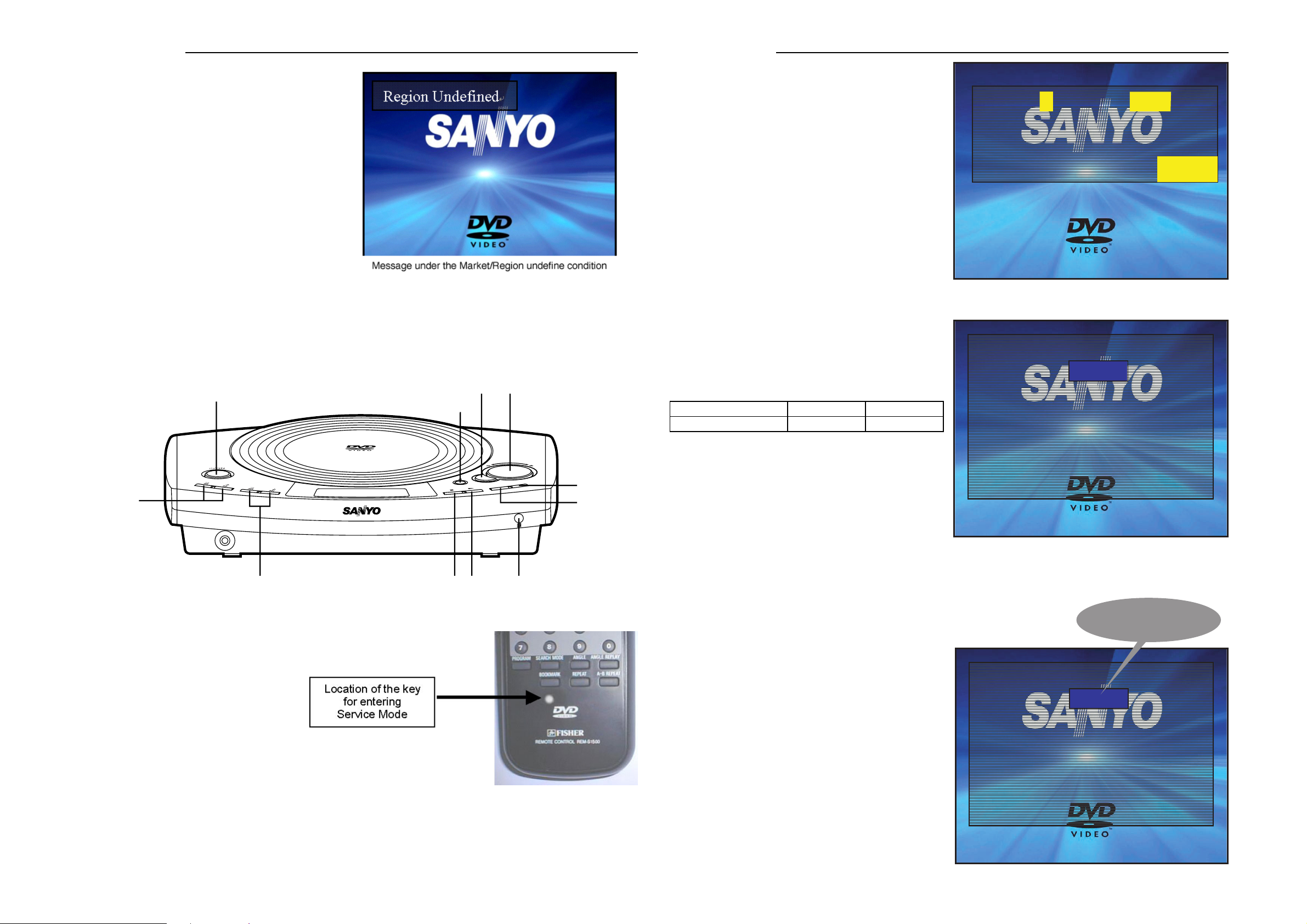
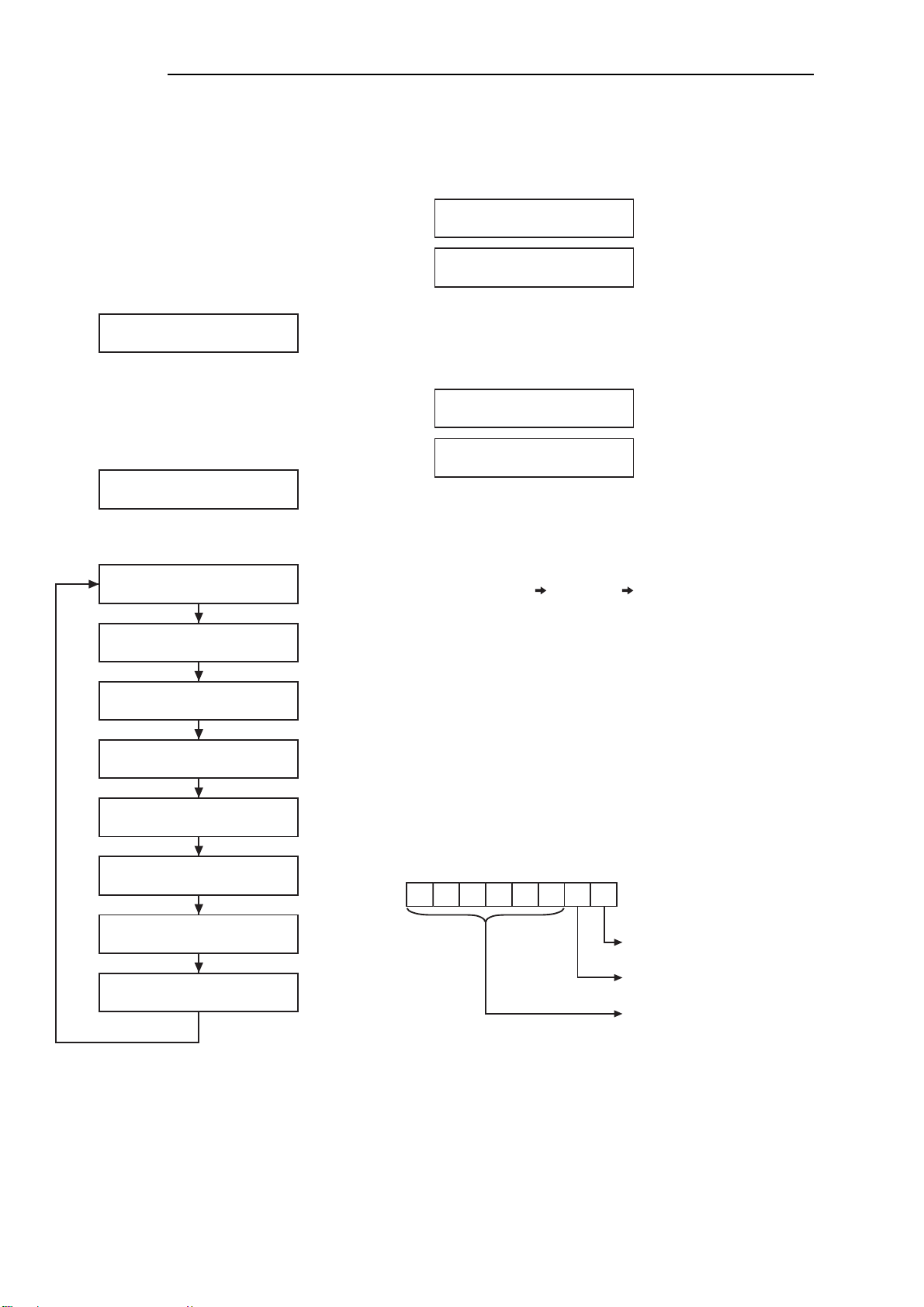
SERVICE MODE
SERVICE MODE
A. Market / Region SETUP
In the initial condition for this model, Market and Region
information are undefined.
In the following cases, be sure to set up Market/Region.
1. When updating the system using CD-R
(Part code : 0PRADC9674--A).
2. When replacing a DVD substrate.
While Market/Region information are undefined, the message
"Region Undefined" is displayed on the screen.
NOTE: Even if the condition is not under 1 or 2 above, if the
message "Region Undefined" is displayed, be sure to set up
Market/Region.
B. How to enter Service Mode.
You can enter Service Mode in any one of the following ways (1 to 3).
1. Using the buttons on the main unit
Immediately (within one second) after pushing both SOUNDand POWER buttons simultaneously, push PLAY button.
SOUND VOLUME
U
M
L
O
E
V
S
O
U
N
D
N
U
D
O
R
R
U
S
N
O
I
T
C
N
U
F
FUNCTION
SURROUND
TUNING,FF/FR
POWER
TUNING
OPEN/CLOSE
P
R
E
SE
T
C. Setup Procedures
1. Displaying SERVICE MODE screen
Display Service Mode screen following the instructions "How to
enter Service Mode" above.
2. Displaying Internal Setup screen
Push NEXT button within three seconds after operating the
Service Mode display.
On the Internal Setup screen shown on the right, set up
Market and Region.
Model Market Region
DC-PT100/XE 03 2
Market/Region setup table.
Region
BackendVersion
LoaderVersion
0
Market
S21225A0
16 Z08 W03
Service Mode Screen
Internal Setup
Markett W M
00
Region 1
00-WM
01-SFC
S18
05-SS 06-PA
02-UK
07-AU 08-CN
WM
03-XE
Value
Exit
04-
09-JP
PHONES
PRESET,SKIP/NEXT/PREVIOUS
2. Pushing the covered key located beneath Book Mark key on RB-
1500 or REM-S1500.
3. Simultaneously pushing both Shift key and ON SCREEN key on
RB-SL30K.
RB-TS760
PT100
IRPLAYSTOP
3. Setting Market code
3.1. While a highlighted indicator is displayed on the right side
of the Market denotation, push numeric buttons on the
remote controller.
When you push wrong number , push CLEAR button.
(The indicator reset to "00")
Be sure to input by double figures.
For example , in SS input 0 and 5.
Internal Setup
Markett W M
Input number
by pushing number keys.
00
Region 1
Exit
3.2. Specify the code of the model in accordance with the
Market/Region Setup Table above.
00-WM
01-SFC
S18
05-SS 06-PA
02-UK
03-XE
07-AU 08-CN
04-
09-JP
3.3 Once the desired code is displayed, push p button to
move the highlighted indicator to the Region input area.
- 5 -- 4 -
Page 5

SERVICE MODE
4. Setting REGION code
4.1 While a highlighted indicator is displayed on the right side
of the Region denotation, push ENT, -> and <- each button
on the remote controller. With each push the indicator will
advance as shown below.
1 <-> 2 <-> 3 <-> 4 <-> 5 <-> 6
4.2 Specify the number of the model in accordance with the
Market/Region Setup Table above.
4.3 Once the desired number is displayed, push p button to
move the highlighted indicator to Exit area.
5. Saving settings
5.1 Make sure that the Market and Region settings are properly
set.
(If any of the settings are incorrect, you can make a change
by moving the indicator using o button, and following
procedures 3 and 4 above. )
5.2 After ensuring that the settings are all correct, push ENT
button while the indicator is on Exit area. The settings are
now saved.
Internal Setup
Market
Region
00
1
00-WM
01-SFC
S18
05-SS 06-PA
02-UK
07-AU 08-CN
Internal Setup
Market
Region
00-WM
01-SFC
S18
05-SS 06-PA
02-UK
07-AU 08-CN
1
00
1
Exit
03-XE
09-JP
Exit
03-XE
09-JP
04-
04-
6. Finishing settings
6.1 After a few seconds, the Internal Setup screen disappears,
and then the Service Mode screen is displayed again for
three seconds as shown on the right.
You should check the settings.
Backend version
Brand (S : SANYO , F : FISHER)
Version ( 2 0 0 2 . 12 . 25)
Sub Version (A,B,......Z)
Region ( 0 : Region undefined
1 ~ 6 : Region defined )
Loader Version (16 Z08 W03)
6.2 Power OFF.
S 21225 A 0
Region
BackendVersion
LoaderVersion
1
Market
16 Z08 W03
WM
S21225A1
Value
Service Mode Sceen after settings
- 6 -
Page 6

SERVICE MODE
D. IMPORTANT NOTE
1. Once the "Market/Region" settings are written into EEPROM (IC801) on the DVD substrate, they cannot be reset.
(However, updating the system using CD-R enables you to make new settings.)
2. While the Internal Setup screen is displayed, pushing the Power button enables you to terminate the operations without
making any settings.
HOW TO LOAD SOFTWARE FOR MPEG P.W.BOARD
1. Power on, then open tray.
2. It take on CD-ROM for UPDATE software to the tray, and tray close.
3. For the time being, tray open and FL display remain "UP DATING".
4. When software loading finished, "GOOD-BY" on a FL display disappears.
5. Next, set up market code and region code by "SERVICE MODE"
CD-ROM part code is "0PRADC9674--A".
CAUTIONS FOR PWB or IC ASSY EXCHANGE
After an MAIN board(614 328 1603) or IC ASSY(410 489 6705) exchange should carry out loading of the software by the
newest CD-R, and should check operation.
- 7 -
Page 7
TUNER ADJUSTMENT
• Use a plastic screw driver for adjustments. • MODE : ST (Stereo)
• Speaker impedance : 8 ohms • TUNING FM : 87.5 - 108MHz
AM : 522 - 1611 kHz
FM DET
TP24
C2315
C2305
C2306
R2306
C2461
C2462
IC241
LC72121M
C2456
R2453
XF233
C2463
C2464
20
C2455
R2452
C2307
C2452
AM DET
0V-TP2
0V ADJ
0V-TP1
TP25
IC231
R2303
R2308
R2303
C2308
C2314
C2316
C2312
C2309
R2309
C2310
C2318
242013
R2307
LA1844
C2320
IC231
C2319
C2302
C2330
C2117
R2302
12 10
1
C2301
R2304
C2303
1210
C2304
0V ADJ
C2322
R2305
13
R2458
R2114
C2451
XF231XF233 TP24
CN291
C2904
JW201
HP-SW2
SG291
C2901
C2902
C2903
SG293SG292
HP-R2 HP-R1
HP.GND2
HP-SW1
L2903
HP-MUT
TP13TP14
L2902
CN241
HP-L2
L2901
HP-L1
HP.GND1
TU-LTU-R
Q2902
Q2901
R2901
HP-L
GND
R2902
HP-R
HP.GND
DI
DO
1AD4B10D2011A
5.6V
+12V
HP_SW
HP_MUT
TP15
94V-0 F01
TU-L
TU-R
TU.GND
GND
+12V
CLK
CE
5.6V
RDS IO0
TP26
C2465
X2451
Q2451
C2317
C2321
CAN
1
24
C2454
C2453
C2457
C2327
C2328
R2811
R2812
R2711
R2712
L2503
DI
DO
CE
CLK
C2991
NC(GND)
D2451
D2301
C2992
R2301
R2461
R2462
R2311
R2463
R2464
L2451
R2455
D2452
R2459
R2465R2454
C2311
XF222
XF231
L2102
12
TP11(H)
TP12(E)
TP11
L2102 L2101
R2101
L2103
TA8176S
XF221
IC211
C2104
R2113
C2126
C2105
R2112
C2111
R2104
C2107
R2102
R2103
C2106
D2102 D2101
TP11(H)
C2113
CAN
C2151
C2152
R2151
R2153
TP25
C2112C2109
L2101
C2108
R2111
C2123
C2101
R2106
C2102
TP12(E)
1
FM.GND
FM-ANT
AM-ANT
AM.GND
TP12
C2130
C2121
C2103
SH201
XF211
D2104
C2122
L2151
B2101
D2151
CN203
CN201
C2131
TP12
L2151-aTP11
1. FM
Adjusting
Step
Circuit
1
Adjustment
2
Cover
Tracking3
4
Auto Stop
2. AM
Adjusting
Step
Circuit
1
Adjustment
Cover
2
Voltage
3 Tracking
Antenna : 75Ω unbalanced direct, Modulation : 1 kHz
Dev. : ±22.5kHz(MONO), ±22.5kHz(STEREO),±6.75kHz(PILOT)
RF Level : dBuV EMF
Output Level : about 100mV at TP13, TP14, TP15
Connection
Input Output
IF
FM Ant
IC231 3-22Pin
TP24,25
TP11 (H)
---
TP12 (E)
---
TP13 (L)
FM Ant L2101 Maximum
TP14 (R)
TP15 (E)
FM Ant -- -
SG
Frequency
Adjustment
98.0MHz XF233
87.5MHz
108.0MHz
L2102
---
90.0MHz
106.0MHz
98.0MHz
L2101
Remark
0.0±0.05V
1.1±0.1V
Confirm voltage of 108.0MHz is
about 7.5V.
Confirm Auto Stop SENS.
If SENS is bad,align L2101
Anntena : IRE Loop(SG), Moduration : 1kHz 30%
RF Level : dBuV EMF
Output Level : about 100mV at TP13, TP14, TP15
Connection
Input
IF
Loop Ant
Output
IC231 19Pin_DCCUT
(TP26)-GND
TP11 (H)
-- TP12 (E) 1611kHz
TP13 (L)
Loop Ant L2151-a
TP14 (R)
TP15 (E)
- 8 -
SG
Frequency
Adjustment
522kHz XF231
522kHz
603kHz
1404kHz
Remark
Maximum
Confirm voltage is > 0.8V.
--Confirm voltage is > 9.0V.
Maximum
Page 8
TUNER SETUP
1. DESTINATION SETTING
1.1 Press "POWER" button to turn on the power.
1.2 Change to "AUX Function" or "DVD/CD Function".
1.3 Press "SOUND" button and "POWER" button on the
main unit at the same time.
1.4 Release "SOUND" button and "POWER" button at the
same time, then within 1 second, press
"TUNING(REV)" button on the main unit.
1.5 The present tuner destination appears on the LCD.
(See Fig.1)
(It appears for 3 seconds on the LCD)
US
(Fig.1)
2. DESTINATION CHANGING
2.1 While the tuner destination appears on the LCD for 3
seconds, press "STOP" button. (Fig.1)
2.2 Tuner destination can be changed at this stage.(Fig.2)
LCD display will not disappear even after 3 seconds.
US
2.3 Whenever the "+TUNING(FWD)" button on the main
unit is pressed, the tuner destination will be changed.
(Fig.2)
US
*
EU2 R
SS K
3. RDS FUNCTION and KARAOKE FUNCTION
SETTING
3.1 When the tuner destination selects, RDS function can
be selected by pressing "PRESET(PREV)" button on
the main unit.
*
EU2 R
EU2
This model setting is "EU2 R".
*
3.2 When the tuner destination selects, KARAOKE
function can be selected by pressing
"PRESET(NEXT)" button on the main unit.
SS K
SS
This model has no KARAOKE function.
*
3.3 After "Tuner Destination", "RDS function" and
"KARAOKE function" is selected, press "POWER"
button on the main unit 3 times.
(POWER OFF POWER ON POWER OFF)
Unplug and plug in the AC cord after that.
And check on the accuracy of the each setting.
*TUNER initial setting
Destination "EU2" and "EU3" : RDS function "YES"
Destination "SS" : KARAOKE function "YES"
Here is the end. All settings are determined.
RDS function YES
RDS function NO
KARAOKE function YES
KARAOKE function NO
JP2
NXJP
NXJPTV
EU3 R
SSJP2+
(Fig.3)
This model setting is "EU2 R".
*
2.4 After the tuner destination is selected, press "POWER"
button on the main unit 3 times.
(POWER OFF POWER ON POWER OFF)
Unplug and plug in the AC cord after that.
And check on the accuracy of the each setting.
* NOTES
1. Tuner destination display can be changed while
tuner functions.
2. Tuner destination setting can be initialized by RAM
CLEAR (Initialization).
LCD DISPLAY
KARAOKE function
"K" = KARAOKE function "YES"
RDS function
"R" = RDS function "YES"
Destination
- 9 -
Page 9
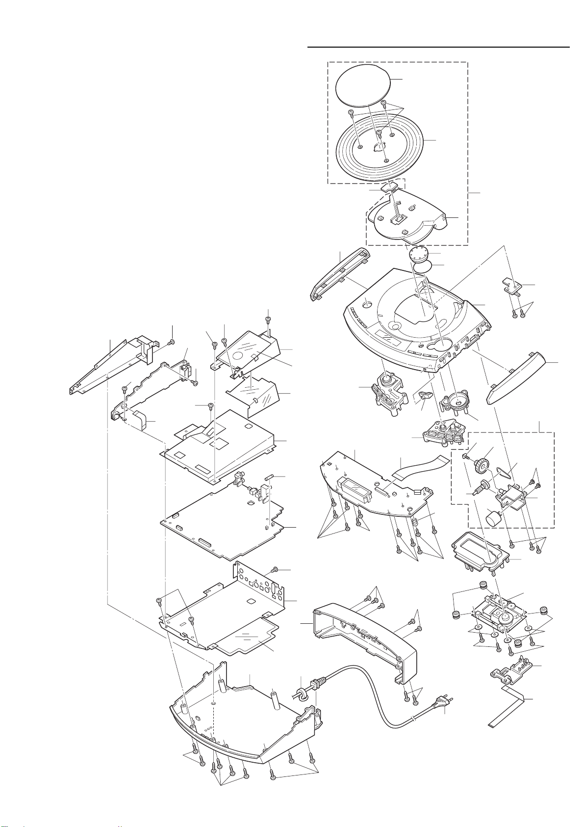
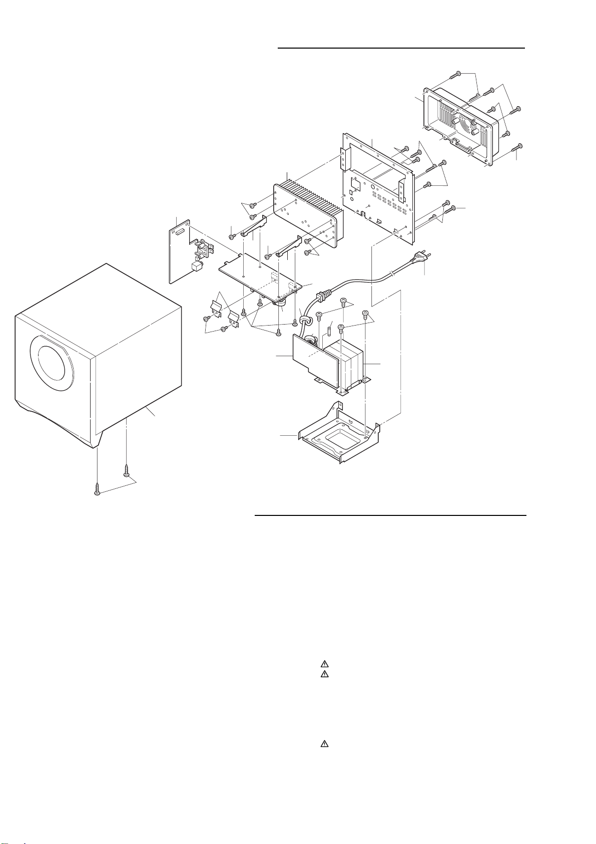
EXPLODED VIEW (CABINET & CHASSIS)
1
Y01
2
25
Y12
53
Y09
74
Y12
Y12
Y10
Y11
Y12
29
54
26
27
28
71
8
10
73
11
51
5
6
12
4
3
72
16
Y02
9
14
Y04
13
Y03
7
15
Y17
Y14
Y17
33
31
Y13
32
75
30
55
Y06
Y17
- 10 -
Y06
Y15
17
19
Y07
Y08
Y06
Y15
20
Y06
22
Y16
56
This is a basic exploded view.
18
Y05
21
34
23
Y07
Y08
24
52
Page 10

PARTS LIST
PRODUCT SAFETY NOTICE
EACH PRECAUTION IN THIS MANUAL SHOULD BE FOLLOWED DURING SERVICING. COMPONENTS IDENTIFIED WITH THE
!!
IEC SYMBOL
PERFORMANCE CAN BE OF SPECIAL SIGNIFICANCE. WHEN REPLACING A COMPONENT IDENTIFIED BY
REPLACEMENT PARTS DESIGNATED, OR PARTS WITH THE SAME RATINGS OF RESISTANCE, WATTAGE OR VOLTAGE THAT
ARE DESIGNATED IN THE PARTS LIST IN THIS MANUAL. LEAKAGE-CURRENT OR RESISTANCE MEASUREMENTS MUST BE
MADE TO DETERMINE THAT EXPOSED PARTS ARE ACCEPTABLY INSULATED FROM THE SUPPLY CIRCUIT BEFORE
RETURNING THE PRODUCT TO THE CUSTOMER.
CAUTION : Regular type resistors and capacitors are not listed. To know those values, refer to the schematic diagram.
N.S.P : Not available as service parts.
!
IN THE PARTS LIST AND THE SCHEMATIC DIAGRAM DESIGNATED COMPONENTS IN WHICH SAFETY AND
!!
!
, USE ONLY THE
Regular type resistors are less than 1/4 W carbon type and 0 ohm chip resistors.
Regular type capacitors are less than 50 V and less than 1000 µF type of Ceramic type and Electrical type.
PACKING & ACCESSORIES
REF.NO. PART NO. DESCRIPTION
614 328 5175 CARTON CASE
614 327 1673 CUSHION,L
614 327 1680 CUSHION,R
614 328 5205 INSTRUCTION MANUAL
614 329 5419 INSTRUCTION MANUAL,GREEK
645 041 1533 POLY SHEET-0750X0500*NC,SET
645 045 3540 POLY SHEET-1100X0600*NC,
SPEAKER
614 229 4635 FM ANTENNA
or 614 308 5515 FM ANTENNA
645 063 4031 LOOP,AM LOOP ANTENNA
645 064 7819 REMOCON,RB-PT100RDS
645 063 5052 CABLE,AUDIO
or 645 064 7994 CABLE,AUDIO
614 327 5664 ASSY,WIRE
645 066 9330 CABLE,VIDEO
614 329 0995 ASSY,BOX,SPEAKER,FRONT
CABINET & CHASSIS
REF.NO. PART NO. DESCRIPTION
1 614 329 6188 DEC,SHEET,DVD
2 614 327 1468 DEC,WINDOW DVD
3 614 327 1574 LID,DVD
4 614 328 5069 ASSY,LID DVD
or 614 329 6157 ASSY,LID,DVD
5 614 327 1567 KNOB,VR,VOL.
6 614 328 4475 DEC,SHEET,JOG,
CAB.TOP-KNOB,VR
7 614 327 1338 ASSY,CABINET,TOP
8 614 327 1598 PANEL,SIDE,L
9 614 327 1604 PANEL,SIDE,R
10 614 327 2595 ASSY,BUTTON,L
11 614 327 2601 ASSY,BUTTON,R
12 614 327 1499 DEC,WINDOW,IR
13 614 327 1475 DEC,RING,VOL.
14 614 327 2625 ASSY,MOUNTING,GEAR
15 614 327 1536 GEAR,HERI-SPUR
16 614 327 1406 BELT,SQUARE
17 614 327 1543 GEAR,WORM-PULLEY
18 614 327 1581 MOUNTING,GEAR
19 645 032 5861 MOTOR,DC 0.2W
20 614 327 5541 SPRING,COMP,PWB,TOP
21 614 327 1451 COVER,MECHA,DVD
22 614 301 1552 SPACER,MECHA,DVD,MECHA
23 614 310 3899 SPACER,MECHA,DVD MECHA
24 614 327 1529 FIXER,PICK,FFC,DVD MECHA
25 614 327 1642 SHIELD,TU,L,TU PWB
26 614 327 4681 SHIELD,PWB,POWER,DVD
27 614 328 2150 SPACER,SHIELD
28 614 327 4674 SPACER,COVER,
DVD(POWER) PWB
29 614 327 1628 SHIELD,DVD,TOP,DVD PWB
30 614 327 1635 SHIELD,DVD,BOTTOM,DVD PWB
31 614 328 4109 SPACER,PWB,BOTTOM,SHIELD
32 614 327 1437 CABINET,REAR
REF.NO. PART NO. DESCRIPTION
33 614 327 2618 ASSY,CABINET,BOTTOM
34 614 327 4438 500AVST3 SE BA,
MECHANISM ASSY
FIXING PARTS
REF.NO. PART NO. DESCRIPTION
Y01 411 021 6405 SCR S-TPG BIN 3X8,LID+WINDOW
Y02 411 165 3803 SCR S-TPG BIN 2.3X10,SW PWB
Y03 411 187 1801 SCR S-TPG PAN+FLG 2X10,GEAR
Y04 411 044 7502 SCR PAN+SW 2X5,MOTOR
Y05 411 165 3803 SCR S-TPG BIN 2.3X10,ASSY,GEAR
Y06 411 165 3803 SCR S-TPG BIN 2.3X10,TOP PWB
Y07 411 092 0906 WASHER Z 2.6X10X0.5,DVD MECHA
Y08 411 021 1806 SCR S-TPG BIN 2.6X10,DVD MECHA
Y09 411 021 4104 SCR S-TPG BIN 3X12,
TU PWB+SHIELD
Y10 411 021 6405 SCR S-TPG BIN 3X8,
TU PWB+SHIELD
Y11 411 021 6405 SCR S-TPG BIN 3X8,
SHIELD,PWR+BOTTOM
Y12 411 021 6405 SCR S-TPG BIN 3X8,
DVD PWB-SHIELD
Y13 411 021 4104 SCR S-TPG BIN 3X12,
DVD PWB-SHIELD
Y14 411 021 6405 SCR S-TPG BIN 3X8,
SHIELD+BOTTOM
Y15 411 021 4104 SCR S-TPG BIN 3X12,
REAR+SOCKET
Y16 411 021 4005 SCR S-TPG BIN 3X12,
BOTTOM+REAR
Y17 411 021 4005 SCR S-TPG BIN 3X12,
TOP+BOTTOM
ELECTRICAL PARTS
REF.NO. PART NO. DESCRIPTION
51 645 061 4422 FLEXIBLE FLAT CABLE,
MAIN-FRONT(28P)
52 645 061 4637 FLEXIBLE FLAT CABLE,
MAIN-PICK(24P)
53 645 061 4415 FLEXIBLE FLAT CABLE,
MAIN-TUNER(15P)
54 423 028 8207 FUSE 250V 1A,250V 1A
55 645 051 0649 CORE,FERRITE,FOR AC CORD
or 645 031 7637 CORE,FERRITE,FOR AC CORD
56 645 061 4965 CORD,POWER-1.76MK,FOR XE
- 11 -
Page 11

PARTS LIST
LED P.W.BOARD ASSY
REF.NO. PART NO. DESCRIPTION
71 614 327 2670 ASSY,PWB,LED(Only initial)
D6901 408 052 7808 LED SECU4L01C*,AQUA BLUE
D6902 408 052 7709 LED SECU4E01C*,BLUE
SWITCH P.W.BOARD ASSY
REF.NO. PART NO. DESCRIPTION
72 614 328 1955 ASSY,PWB,SW(Only initial)
CN681 645 005 8134 PLUG,8P
CN682 645 038 4035 PLUG,3P
CN683 645 017 0713 PLUG,2P
S6801 645 057 5785 SWITCH,LEVER
FRONT P.W.BOARD ASSY
REF.NO. PART NO. DESCRIPTION
73 614 327 2786 ASSY,PWB,FRONT(Only initial)
BRC60 614 327 1444 COVER,LED
BRH60 614 327 1550 HOLDER,LCD
BRS60 614 327 1512 DEC,SHEET,LCD
CN601 645 062 2618 SOCKET,FPC 28P
CN603 645 006 0908 PLUG,2P
CN604 645 061 4569 SOCKET,FPC 11P
CN605 614 327 6470 ASSY,WIRE
CN606 645 004 2683 PLUG,2P
D6000 407 012 4406 DIODE 1SS133
D6001 407 012 4406 DIODE 1SS133
D6002 407 012 4406 DIODE 1SS133
D6003 407 012 4406 DIODE 1SS133
D6021 407 099 9103 ZENER DIODE MTZJ27B
D6070 407 233 4803 LED SELU2L10C
DS601 407 233 3806 PHOTO DIODE SPS-447-1-VG
IC601 409 350 8009 IC LC75854E
LCD60 645 061 4521 LCD
Q6032 405 109 9204 TR KRC102M-A
or 405 000 3103 TR DTC114ES
Q6033 405 109 9204 TR KRC102M-A
or 405 000 3103 TR DTC114ES
Q6071 405 109 9204 TR KRC102M-A
or 405 000 3103 TR DTC114ES
Q6072 405 110 5400 TR KRA102M-A
or 405 000 0508 TR DTA114ES
S6001 645 037 2759 SWITCH,PUSH
or 645 006 5958 SWITCH,PUSH 1P-1T
or 614 220 5471 SWITCH,TACT
or 614 240 1002 SWITCH,TACT
S6002 645 037 2759 SWITCH,PUSH
or 645 006 5958 SWITCH,PUSH 1P-1T
or 614 220 5471 SWITCH,TACT
or 614 240 1002 SWITCH,TACT
S6003 645 037 2759 SWITCH,PUSH
or 645 006 5958 SWITCH,PUSH 1P-1T
or 614 220 5471 SWITCH,TACT
or 614 240 1002 SWITCH,TACT
S6004 645 037 2759 SWITCH,PUSH
or 645 006 5958 SWITCH,PUSH 1P-1T
or 614 220 5471 SWITCH,TACT
or 614 240 1002 SWITCH,TACT
S6005 645 037 2759 SWITCH,PUSH
or 645 006 5958 SWITCH,PUSH 1P-1T
or 614 220 5471 SWITCH,TACT
or 614 240 1002 SWITCH,TACT
S6006 645 037 2759 SWITCH,PUSH
or 645 006 5958 SWITCH,PUSH 1P-1T
or 614 220 5471 SWITCH,TACT
or 614 240 1002 SWITCH,TACT
S6007 645 037 2759 SWITCH,PUSH
or 645 006 5958 SWITCH,PUSH 1P-1T
or 614 220 5471 SWITCH,TACT
or 614 240 1002 SWITCH,TACT
REF.NO. PART NO. DESCRIPTION
S6008 645 037 2759 SWITCH,PUSH
or 645 006 5958 SWITCH,PUSH 1P-1T
or 614 220 5471 SWITCH,TACT
or 614 240 1002 SWITCH,TACT
S6009 645 037 2759 SWITCH,PUSH
or 645 006 5958 SWITCH,PUSH 1P-1T
or 614 220 5471 SWITCH,TACT
or 614 240 1002 SWITCH,TACT
S6010 645 037 2759 SWITCH,PUSH
or 645 006 5958 SWITCH,PUSH 1P-1T
or 614 220 5471 SWITCH,TACT
or 614 240 1002 SWITCH,TACT
S6011 645 037 2759 SWITCH,PUSH
or 645 006 5958 SWITCH,PUSH 1P-1T
or 614 220 5471 SWITCH,TACT
or 614 240 1002 SWITCH,TACT
S6050 645 031 8078 SWITCH,ROTARY(ENCODER)
TUNER P.W.BOARD ASSY
REF.NO. PART NO. DESCRIPTION
74 614 328 4222 ASSY,PWB,TUNER(Only initial)
B2101 645 006 3602 INDUCTOR,1.1UH
CN201 645 057 1909 TERMINAL,TUNER
CN203 645 004 2683 PLUG,2P
CN241 645 059 0481 SOCKET,FPC 15P
CN291 645 031 4315 JACK,PHONE D3.6
D2151 407 149 0807 DIODE 1SS355
D2301 407 063 9108 ZENER DIODE MTZJ6.8B
D2451 407 149 0807 DIODE 1SS355
D2452 407 153 7502 ZENER DIODE GZS3.0B
D2466 407 221 1906 DIODE KDS121E
or 407 162 8507 DIODE DAN222
IC231 409 474 3201 IC LA1844ML
IC241 409 439 4502 IC LC72121M-D
IC251 409 447 3900 IC LC72722
L2151 645 063 0163 TUNER
L2451 645 001 4581 INDUCTOR,100U K
L2501 645 001 4581 INDUCTOR,100U K
L2502 645 001 4581 INDUCTOR,100U K
L2503 645 004 0511 INDUCTOR,270U J
L2901 645 006 9864 INDUCTOR,80U
L2902 645 006 9864 INDUCTOR,80U
L2903 645 001 4550 INDUCTOR,10U K
LG201 614 129 9082 LUG,HP-GNDTOBOTTOM-GND
Q2140 405 146 2107 TR KTC3875-Y
or 405 146 2206 TR KTC3875-GR
or 405 014 4509 TR 2SC2412K-R
or 405 011 1006 TR 2SC1623-L6
Q2201 405 151 4202 TR KTC3193-O
or 405 151 4103 TR KTC3193-Y
or 405 016 0806 TR 2SC2839-E
Q2310 405 146 2107 TR KTC3875-Y
or 405 146 2206 TR KTC3875-GR
or 405 014 4509 TR 2SC2412K-R
or 405 011 1006 TR 2SC1623-L6
Q2451 405 151 6107 TR KRA107S
or 405 141 5707 TR DTA114YKA
Q2502 405 151 6107 TR KRA107S
or 405 141 5707 TR DTA114YKA
Q2901 405 166 7007 TR KTD1304
Q2902 405 166 7007 TR KTD1304
SG291 645 055 3202 SURGE-ABSORBER
SG292 645 055 3202 SURGE-ABSORBER
SG293 645 055 3202 SURGE-ABSORBER
U2101 645 043 6697 TUNER,FM
X2451 645 023 4965 OSC,CRYSTAL 7.2MHZ
X2501 645 035 8326 OSC,CRYSTAL 4.332MHZ
XF221 645 010 0079 CERAMIC FILTER 10.70MHZ
or 614 240 2917 FILTER,CERAM
or 614 254 3214 FILTER
- 12 -
Page 12
PARTS LIST
REF.NO. PART NO. DESCRIPTION
XF222 645 010 0079 CERAMIC FILTER 10.70MHZ
or 614 240 2917 FILTER,CERAM
or 614 254 3214 FILTER
XF231 614 246 0849 FILTER
XF233 645 039 9923 TRANS,IF 10.7MHZ
MAIN P.W.BOARD ASSY
REF.NO. PART NO. DESCRIPTION
75 614 328 1603 ASSY,PWB,MAIN(Only initial)
C4905 403 260 3505 ELECT 10U M 400V
or 403 395 9007 ELECT 10U M 400V
C4907 404 088 7409 MT-POLYEST 0.1U K 250V
or 404 080 8206 MT-POLYEST 0.1U K 250V
or 403 376 2409 MT-POLYEST 0.1U M 250V
C4908 404 080 8107 CERAMIC 2200P M 400V
C4909 404 080 8107 CERAMIC 2200P M 400V
C4911 404 088 7409 MT-POLYEST 0.1U K 250V
or 404 080 8206 MT-POLYEST 0.1U K 250V
or 403 376 2409 MT-POLYEST 0.1U M 250V
C4921 403 348 1508 MT-POLYEST 0.022U K 400V
C4958 403 184 9003 MT-POLYEST 0.022U J 50V
CN100 645 057 2951 SOCKET,FPC 24P
or 645 037 6207 SOCKET,FFC 24P
CN480 645 061 4453 JACK,RCA-2
or 645 068 3862 JACK,RCA-2
CN481 645 059 0481 SOCKET,FPC 15P
CN482 645 062 2601 SOCKET,FPC 28P
CN483 645 063 9098 JACK,PHONE D3.6
CN484 645 006 1882 PLUG,3P
CN870 645 057 9325 TERMINAL,BOARD,
S/COMPOSITE(W-SHIELD)
CN871 407 234 1801 PHOTO COUPLE GP1FA513TZM
D4700 407 012 4406 DIODE 1SS133
D4701 407 012 4406 DIODE 1SS133
D4780 407 012 4406 DIODE 1SS133
D4850 407 099 6003 ZENER DIODE MTZJ9.1B
D4902 407 012 4406 DIODE 1SS133
D4903 407 099 5303 ZENER DIODE MTZJ5.6B
D4904 407 004 9808 DIODE DSK10E
or 407 012 0408 DIODE 1N4004
or 407 004 9808 DIODE DSK10E
D4905 407 004 9808 DIODE DSK10E
or 407 012 0408 DIODE 1N4004
or 407 004 9808 DIODE DSK10E
D4906 407 004 9808 DIODE DSK10E
or 407 012 0408 DIODE 1N4004
or 407 004 9808 DIODE DSK10E
D4907 407 004 9808 DIODE DSK10E
or 407 012 0408 DIODE 1N4004
or 407 004 9808 DIODE DSK10E
D4921 408 043 6803 DIODE RGP02-15EL-22C-012
D4950 408 043 6704 DIODE RGP10GL-22C-012
D4951 407 099 6607 ZENER DIODE MTZJ12B
D4952 408 044 7304 DIODE SB160L-19C2-004
D4953 408 044 6307 DIODE SB140L 19C2-004
D4954 408 043 6704 DIODE RGP10GL-22C-012
D4955 407 099 6607 ZENER DIODE MTZJ12B
FPC41 645 031 7903 HOLDER,FUSE
or 645 006 4760 HOLDER,FUSE
FPC42 645 031 7903 HOLDER,FUSE
or 645 006 4760 HOLDER,FUSE
IC100 409 564 4507 IC LA9703WLS-MPB
or 409 518 1507 IC LA9703WL-MPB
IC130 409 564 5702 IC LC78663NRW-UST
or 409 531 6107 IC LC78663NRW
IC131 410 433 0308 IC M11L416256SA-35T
IC160 409 478 0800 IC BA5937AFP
IC161 409 405 6301 IC BA6849FP
IC411 409 357 2901 IC NJM4556AL
IC470 410 500 6509 IC M38507M8-168FP,MICON
IC471 410 448 8405 IC S524A40X21-SCT0,EEPROM
or 410 448 8504 IC S524A40X21-SCB0,EEPROM
or 410 429 7908 IC AT24C02N-10SI-2.7,EEPROM
REF.NO. PART NO. DESCRIPTION
IC472 409 543 6409 IC KRX101U
IC473 409 505 0803 IC PST3627U,RESET
IC480 409 474 6103 IC LC75342M
IC481 409 448 7402 IC LA2610
IC490 409 573 5601 IC STR-A6151
IC492 409 517 5704 IC KA431AZTF
or 409 508 2804 IC KIA431A
or 409 508 2705 IC KIA431
or 409 067 7203 IC L5431
IC493 409 543 0100 IC PQ1X501M2Z
IC494 409 509 9208 IC PQ070XZ01Z
IC495 409 534 5800 IC PQ2L2182MS
IC800 409 546 2002 IC ZR36748
IC801 410 448 8405 IC S524A40X21-SCT0
or 410 448 8504 IC S524A40X21-SCB0
or 410 429 7908 IC AT24C02N-10SI-2.7
IC802 409 505 0803 IC PST3627U
IC806 410 430 9403 IC 74VHCT08AMTCX
IC818 410 489 6705 IC ASSY
(IC SST39VF800A-70-4C-EK or
SST39VF800-70-4C-EK or
LE28DW8163T-70T-MPB or
SST39VF800A-70-4C-EK,D)
IC822 410 470 5007 IC M12L16161A-7T
or 410 453 9602 IC LC3816161ET-70-MPB
or 409 482 0209 IC K4S161622D-TC80
or 409 482 0209 IC K4S161622D-TC80
IC859 409 489 9700 IC NC7SZ157P6
IC871 409 581 9400 IC PCM1755DBQ,DAC_2CH
IC881 409 543 6409 IC KRX101U
L1000 645 034 7887 INDUCTOR,1000 OHM
or 645 020 1813 INDUCTOR,1000 OHM
or 645 045 7869 IMPEDANCE,1000 OHM P
or 645 020 2001 INDUCTOR,1000 OHM
L1002 645 034 7887 INDUCTOR,1000 OHM
or 645 020 1813 INDUCTOR,1000 OHM
or 645 045 7869 IMPEDANCE,1000 OHM P
or 645 020 2001 INDUCTOR,1000 OHM
L1302 645 034 7887 INDUCTOR,1000 OHM
or 645 020 1813 INDUCTOR,1000 OHM
or 645 045 7869 IMPEDANCE,1000 OHM P
or 645 020 2001 INDUCTOR,1000 OHM
L4700 645 001 4550 INDUCTOR,10U K
L4750 645 020 1882 INDUCTOR,1800 OHM
L4751 645 020 1882 INDUCTOR,1800 OHM
L4752 645 020 1882 INDUCTOR,1800 OHM
L4753 645 020 1882 INDUCTOR,1800 OHM
L4754 645 020 1882 INDUCTOR,1800 OHM
L4755 645 020 1882 INDUCTOR,1800 OHM
L4756 645 020 1882 INDUCTOR,1800 OHM
L4757 645 020 1882 INDUCTOR,1800 OHM
L4758 645 020 1882 INDUCTOR,1800 OHM
L4840 645 034 7887 INDUCTOR,1000 OHM
or 645 020 1813 INDUCTOR,1000 OHM
or 645 045 7869 IMPEDANCE,1000 OHM P
or 645 020 2001 INDUCTOR,1000 OHM
L4841 645 034 7887 INDUCTOR,1000 OHM
or 645 020 1813 INDUCTOR,1000 OHM
or 645 045 7869 IMPEDANCE,1000 OHM P
or 645 020 2001 INDUCTOR,1000 OHM
L4900 645 057 4030 LINE FILTER
or 645 045 8941 LINE FILTER
or 645 038 2024 LINE FILTER
L4950 645 048 4469 INDUCTOR,22U
or 645 045 8613 INDUCTOR,10U
L4951 645 048 4469 INDUCTOR,22U
or 645 045 8613 INDUCTOR,10U
L8060 645 034 7887 INDUCTOR,1000 OHM
or 645 020 1813 INDUCTOR,1000 OHM
or 645 045 7869 IMPEDANCE,1000 OHM P
or 645 020 2001 INDUCTOR,1000 OHM
- 13 -
Page 13
PARTS LIST
REF.NO. PART NO. DESCRIPTION
L8202 645 034 7887 INDUCTOR,1000 OHM
or 645 020 1813 INDUCTOR,1000 OHM
or 645 045 7869 IMPEDANCE,1000 OHM P
or 645 020 2001 INDUCTOR,1000 OHM
L8410 645 040 6430 INDUCTOR,2.2U M
L8420 645 040 6430 INDUCTOR,2.2U M
L8440 645 040 6430 INDUCTOR,2.2U M
L8582 645 034 7887 INDUCTOR,1000 OHM
or 645 020 1813 INDUCTOR,1000 OHM
or 645 045 7869 IMPEDANCE,1000 OHM P
or 645 020 2001 INDUCTOR,1000 OHM
L8701 645 034 7887 INDUCTOR,1000 OHM
or 645 020 1813 INDUCTOR,1000 OHM
or 645 045 7869 IMPEDANCE,1000 OHM P
or 645 020 2001 INDUCTOR,1000 OHM
PC490 407 234 8800 PHOTO COUPLE PC123X2YFZ
or 407 220 4601 PHOTO COUPLE PC123Y22
or 407 203 8602 PC PS2561-1-V
or 407 234 8800 PHOTO COUPLE PC123X2YFZ
PR480 645 042 2515 PROTECTOR,0.2A 125V
PR490 645 042 2553 PROTECTOR,0.63A 125V
PR491 645 042 2553 PROTECTOR,0.63A 125V
PT490 645 061 7812 TRANS,POWER,PULSE
Q1002 405 146 2107 TR KTC3875-Y
or 405 146 2206 TR KTC3875-GR
or 405 014 4509 TR 2SC2412K-R
or 405 011 1006 TR 2SC1623-L6
Q1003 405 146 2107 TR KTC3875-Y
or 405 146 2206 TR KTC3875-GR
or 405 014 4509 TR 2SC2412K-R
or 405 011 1006 TR 2SC1623-L6
Q1004 405 146 2107 TR KTC3875-Y
or 405 146 2206 TR KTC3875-GR
or 405 014 4509 TR 2SC2412K-R
or 405 011 1006 TR 2SC1623-L6
Q1005 405 158 5905 TR KTA1505-Y
or 405 035 5509 TR 2SA1036K-R
Q1006 405 158 5905 TR KTA1505-Y
or 405 035 5509 TR 2SA1036K-R
Q1016 405 146 2107 TR KTC3875-Y
or 405 146 2206 TR KTC3875-GR
or 405 014 4509 TR 2SC2412K-R
or 405 011 1006 TR 2SC1623-L6
Q1550 405 146 2107 TR KTC3875-Y
or 405 146 2206 TR KTC3875-GR
or 405 014 4509 TR 2SC2412K-R
or 405 011 1006 TR 2SC1623-L6
Q1551 405 146 2107 TR KTC3875-Y
or 405 146 2206 TR KTC3875-GR
or 405 014 4509 TR 2SC2412K-R
or 405 011 1006 TR 2SC1623-L6
Q1660 405 146 2107 TR KTC3875-Y
or 405 146 2206 TR KTC3875-GR
or 405 014 4509 TR 2SC2412K-R
or 405 011 1006 TR 2SC1623-L6
Q1661 405 159 0503 TR KRC107S
or 405 141 5608 TR DTC114YKA
Q4150 405 166 7007 TR KTD1304
Q4151 405 166 7007 TR KTD1304
Q4250 405 166 7007 TR KTD1304
Q4251 405 166 7007 TR KTD1304
Q4720 405 146 2107 TR KTC3875-Y
or 405 146 2206 TR KTC3875-GR
or 405 014 4509 TR 2SC2412K-R
or 405 011 1006 TR 2SC1623-L6
Q4790 405 146 1704 TR KTA1504-Y
or 405 146 9700 TR KTA1504-GR
or 405 134 5905 TR 2SA1037AK-R
or 405 002 0308 TR 2SA1037K-R
or 405 005 5508 TR 2SA812-M6
Q4791 405 159 0503 TR KRC107S
or 405 141 5608 TR DTC114YKA
Q4792 405 151 6107 TR KRA107S
REF.NO. PART NO. DESCRIPTION
or 405 141 5707 TR DTA114YKA
Q4793 405 159 0503 TR KRC107S
or 405 141 5608 TR DTC114YKA
Q4850 405 146 2107 TR KTC3875-Y
or 405 146 2206 TR KTC3875-GR
or 405 014 4509 TR 2SC2412K-R
or 405 011 1006 TR 2SC1623-L6
Q4950 405 141 3109 TR KTC3203-Y
or 405 024 9907 TR 2SD734-F
or 405 025 0200 TR 2SD734-G
Q4953 405 141 3703 TR KTA1271-Y
or 405 008 2405 TR 2SB698-F
or 405 008 2504 TR 2SB698-G
Q4955 405 159 0503 TR KRC107S
or 405 141 5608 TR DTC114YKA
Q4956 405 159 0503 TR KRC107S
or 405 141 5608 TR DTC114YKA
Q4957 405 146 1704 TR KTA1504-Y
or 405 146 9700 TR KTA1504-GR
or 405 134 5905 TR 2SA1037AK-R
or 405 002 0308 TR 2SA1037K-R
or 405 005 5508 TR 2SA812-M6
R4908 402 087 3408 RESISTOR 3.3M J- 1/2W
or 402 078 9501 CARBON 3.3M J- 1/2W
or 402 078 8108 CARBON 3.3M J- 1/2W
RN100 645 057 4252 R-NETWORK 8.2KX4 1/16W
RN101 645 057 4290 R-NETWORK 47KX4 1/16W
RN801 645 057 4238 R-NETWORK 33X4 1/16W
SG480 645 055 3202 SURGE-ABSORBER
SG481 645 055 3202 SURGE-ABSORBER
SG841 645 055 3202 SURGE-ABSORBER
SG842 645 055 3202 SURGE-ABSORBER
SG872 645 055 3202 SURGE-ABSORBER
WR490 614 017 8203 TERMINAL BOARD
WR491 614 017 8203 TERMINAL BOARD
X1500 645 059 7060 OSC,CERAMIC 16.93MHZ
or 645 017 0157 OSC,CERAMIC 16.93MHZ
or 645 065 2479 OSC,CERAMIC 16.93MHZ
X4700 645 053 4393 OSC,CERAMIC 8.00MHZ
X8230 645 053 4270 OSC,CRYSTAL 27.000MHZ
or 645 045 8293 OSC,CRYSTAL 27.000MHZ
- 14 -
Page 14
EXPLODED VIEW (SUB WOOFER SPEAKER )
Y08
Y08
7
Y07
6
5
Y07
Y08
Y08
Y07
Y06
73
Y03
Y05
Y05
4
53
54
Y06
72
Y02
52
Y02
4
3
55
Y04
Y07
56
Y08
71
51
1
2
Y01
PARTS LIST (SUB WOOFER SPEAKER)
SUB WOOFER SPEAKER (ASX-PT100W/XE)
CABINET & CHASSIS
REF.NO. PART NO. DESCRIPTION
1 614 328 9302 ASSY,BOX,SPEAKER,(PROSONIC)
2 614 327 8504 HOLDER,POWER TRANS
3 614 316 1417 MOUNTING,IC,IC-HEAT SINK
4 614 327 8498 HOLDER,PWB
5 614 327 8436 ASSY,HEAT SINK
6 614 328 2105 PANEL,REAR
7 614 327 8474 COVER,HEAT,SINK
FIXING PARTS
REF.NO. PART NO. DESCRIPTION
Y01 411 027 3408 SCR S-TPG BIN 4X16,
HOLDER P.T-SP BOX
Y02 411 001 3905 SCR S-TPG BIN 4X6,PT
Y03 411 021 6405 SCR S-TPG BIN 3X8,IC-HEAT SINK
Y04 411 021 6405 SCR S-TPG BIN 3X8,
PWB-HOLDER PWB
Y05 411 021 6405 SCR S-TPG BIN 3X8,
HOLDER PWB-HEAT SINK
Y06 411 021 3503 SCR S-TPG BIN 3X10
This is a basic exploded view.
REF.NO. PART NO. DESCRIPTION
Y07 411 021 3701 SCR S-TPG BIN 3X10,
HOLDER P.T-P.REAR,
COVER H.S-P.REAR,
E.PARTS-P.REAR
Y08 645 046 8216 SCREW,P.REAR-SP.BOX
ELECTRICAL PARTS
REF.NO. PART NO. DESCRIPTION
51 645 061 4583 TRANS,POWER,PT100_UK
52 423 028 8207 FUSE 250V 1A
53 645 051 0649 CORE,FERRITE,FOR AC CORD
or 645 031 7637 CORE,FERRITE,FOR AC CORD
54 645 051 0656 CORE,FERRITE,FOR CN391
or 645 042 8999 CORE,FERRITE,FOR CN391
55 645 051 0656 CORE,FERRITE,FOR LEAD WIRE
or 645 042 8999 CORE,FERRITE,FOR LEAD WIRE
56 645 063 0255 CORD,POWER-1.76MK,XE
- 15 -
Page 15

PARTS LIST
REF.NO. PART NO. DESCRIPTION
71 614 327 4308 ASSY,PWB,MAIN,PT(Only initial)
C3900 403 349 3303 CERAMIC 0.01U M 250V
or 403 366 7803 CERAMIC 0.01U M 250V
CN390 614 020 1239 SOCKET,4P
CN391 614 328 1993 ASSY,WIRE
D3900 407 012 4406 DIODE 1SS133
FPC38 645 031 7903 HOLDER,FUSE
or 645 006 4760 HOLDER,FUSE
FPC39 645 031 7903 HOLDER,FUSE
or 645 006 4760 HOLDER,FUSE
L3900 645 038 7364 INDUCTOR,70U
or 645 059 0467 INDUCTOR,13U
LUG01 645 006 4425 FIXER
RY390 645 059 0306 RELAY,PRIMARY
or 645 030 5597 RELAY,PRIMARY
or 645 035 6575 RELAY,PRIMARY
WR390 614 017 8203 TERMINAL BOARD
WR391 614 017 8203 TERMINAL BOARD
MAIN P.W.BOARD ASSY
REF.NO. PART NO. DESCRIPTION
72 614 329 5105 ASSY,PWB,MAIN(Only initial)
C3004 403 325 0302 ELECT 2200U M 25V
C3008 403 325 0302 ELECT 2200U M 25V
C3210 403 184 9805 MT-POLYEST 0.22U J 50V
C3211 403 184 9805 MT-POLYEST 0.22U J 50V
C3213 403 184 9805 MT-POLYEST 0.22U J 50V
C3214 403 184 9805 MT-POLYEST 0.22U J 50V
C3405 403 185 0108 MT-POLYEST 0.47U J 50V
C3406 403 185 0108 MT-POLYEST 0.47U J 50V
C3408 403 184 9300 MT-POLYEST 0.047U J 50V
CN302 645 006 1790 PLUG,2P
CN303 645 005 7366 PLUG,2P
CN305 645 063 4864 PLUG,10P
CN311 645 006 1813 PLUG,4P
D3000 407 099 6805 ZENER DIODE MTZJ13B
D3001 407 099 6805 ZENER DIODE MTZJ13B
D3002 407 196 5800 DIODE 1N5402BD82
D3003 407 196 5800 DIODE 1N5402BD82
D3004 407 196 5800 DIODE 1N5402BD82
D3005 407 196 5800 DIODE 1N5402BD82
D3501 407 012 4406 DIODE 1SS133
D3502 407 012 4406 DIODE 1SS133
IC320 409 472 5306 IC LM1876TF
IC330 409 426 1903 IC KIA4558F
or 409 039 7804 IC NJM4558M
IC340 409 521 9200 IC LM4700TF
IC360 409 039 5404 IC NJM2058M
L3200 645 057 4405 INDUCTOR,0.7U
or 645 053 7493 INDUCTOR,0.7U
L3201 645 057 4405 INDUCTOR,0.7U
or 645 053 7493 INDUCTOR,0.7U
L3400 645 057 7673 INDUCTOR,AIR 0.7U
or 645 045 6206 INDUCTOR,AIR 0.7U
PR300 645 042 2515 PROTECTOR,0.2A 125V
PR301 645 042 2515 PROTECTOR,0.2A 125V
PR302 645 042 2652 PROTECTOR,10A 125V
PR303 645 042 2652 PROTECTOR,10A 125V
Q3000 405 143 0007 TR KRC107M
or 405 000 3806 TR DTC114YS
Q3001 405 141 3505 TR KTA1266-Y
or 405 141 3406 TR KTA1266-GR
or 405 004 4502 TR 2SA608-F-NP
or 405 004 5004 TR 2SA608-G-NP
Q3002 405 141 3208 TR KTC3198-Y
or 405 141 3307 TR KTC3198-GR
or 405 019 2708 TR 2SC536-F-NP
or 405 019 3804 TR 2SC536-G-NP
Q3003 405 143 0007 TR KRC107M
or 405 000 3806 TR DTC114YS
REF.NO. PART NO. DESCRIPTIONPOWER TRANSFORMER P.W.BOARD ASSY
Q3200 405 151 4400 TR KTD1303
or 405 021 0204 TR 2SD1012-F-SPA
or 405 021 0600 TR 2SD1012-G-SPA
or 405 033 6706 TR 2SD1468S-R
or 405 033 6805 TR 2SD1468S-S
Q3201 405 151 4400 TR KTD1303
or 405 021 0204 TR 2SD1012-F-SPA
or 405 021 0600 TR 2SD1012-G-SPA
or 405 033 6706 TR 2SD1468S-R
or 405 033 6805 TR 2SD1468S-S
Q3400 405 151 4400 TR KTD1303
or 405 021 0204 TR 2SD1012-F-SPA
or 405 021 0600 TR 2SD1012-G-SPA
or 405 033 6706 TR 2SD1468S-R
or 405 033 6805 TR 2SD1468S-S
Q3500 405 141 3208 TR KTC3198-Y
or 405 141 3307 TR KTC3198-GR
or 405 019 2708 TR 2SC536-F-NP
or 405 019 3804 TR 2SC536-G-NP
Q3501 405 141 3208 TR KTC3198-Y
or 405 141 3307 TR KTC3198-GR
or 405 019 2708 TR 2SC536-F-NP
or 405 019 3804 TR 2SC536-G-NP
R3210 402 082 1300 RESISTOR 4.7 J- 1W
R3211 402 082 1300 RESISTOR 4.7 J- 1W
R3212 402 082 2802 RESISTOR 10 J- 1W
R3213 402 082 2802 RESISTOR 10 J- 1W
R3405 402 082 8606 RESISTOR 2.2 J- 1W
R3406 402 082 2802 RESISTOR 10 J- 1W
TERMINAL P.W.BOARD ASSY
REF.NO. PART NO. DESCRIPTION
73 614 329 5112 ASSY,PWB,TERMINAL(Only initial)
CN370 645 063 9098 JACK,PHONE D3.6
CN371 645 061 6990 TERMINAL,SPEAKER 2P
CN372 645 006 1882 PLUG,3P
CN373 645 005 8493 SOCKET,10P
L3700 645 006 3602 INDUCTOR,1.1UH
L3701 645 006 3602 INDUCTOR,1.1UH
L3702 645 006 3602 INDUCTOR,1.1UH
L3703 645 006 3602 INDUCTOR,1.1UH
- 16 -
Page 16

LCD DISPLAY
LCD60
COM1
COM2
126
COM3
COM4
39
PAD N O.
1
2
3
4
5
6
7
8
9
10
11
12
13
14
15
16
17
18
19
20
COM1
--
--
-1M
2M
3M
DP
4M
4D
DP2
5M
5D
6M
6D
DP1
COL
7M
8M
8D
R
PL
COM2
--
COM2
--
-1N
2N
3N
3C
4N
4L
4C
5N
5L
6N
6L
7E
7N
8N
8L
L
1
COM3
--
--
COM3
-1J
2J
3J
3H
4J
4K
4H
5J
5K
6J
6K
6H
7G
7J
8J
8K
27
COM4
--
--
--
COM4
1I
2I
3I
3B
4I
4A
4B
5I
5A
6I
6A
6B
7F
7I
8I
8A
PAD N O.
21
22
23
24
25
26
27
28
29
30
31
32
33
34
35
36
37
38
39
COM1
MONO
PROG.
RND
7D
AB
REP.
ALL
BASS
3D
SLEEP
OFF
2D
TIME
ON
1D
WMA
MP3
234
COM2
R
1
L
8C
8E
7C
7L
6E
5C
5E
-4E
3L
3E
2C
2L
2E
1C
1L
1E
dts
COM3
8H
8G
7H
7K
6G
5H
5G
4G
3K
3G
2H
2K
2G
1H
1K
1G
DD
P
--
COM4
D
8B
8F
7B
7A
6F
5B
5F
-4F
3A
3F
2B
2A
2F
1B
1A
1F
PL
F
E
COL
56 7
A
J
K
I
GH
L
N
M
C
D
8
D
B
DD
TIME
DP DP1DP2
- 17 -
P
AB
Page 17

IC BLOCK DIAGRAM & DESCRIPTION
IC100 LA9703WL-MPB (DVD Player Frontend Processor)
FSET
PREF
LDON1
N/C
AGOF
AGOF
LDON2
LDON1
RFN
PREF
GU
SGC
AGOF
LDON2
EQ
FC BSTDVD/CD
SGC
SGC
SREF
SGC
SREF
BCA GU
BCA
AGOF
Terminal No Symbole
33
34
35
36
37
38
39
40
41
42
43
44
45
46
47
48
49
50
51
52
53
54
55
56
57
58
59
60
61
62
63
64
Terminal No.
1
2
3
4
5
6
7
8
9
10
11
12
13
14
15
16
17
18
19
20
21
22
23
24
25
26
27
28
29
30
31
32
CAP
VCC
PDRF
PD1
PD2
PD3
PD4
GND
FIN1
FIN2
PIN1
PIN2
TIN1
TIN2
LDD1
LDS1
Symbole
CAP
VCC
PDRF
PD1
PD2
PD3
PD4
GND
FIN1
FIN2
PIN1
PIN2
TIN1
TIN2
LDD1
LDS1
LDD2
LDS2
GND
LDTH
LDON1
LDON2
AGOF
BCA
GU
DVD/CD
DPD/TE
WO/PP
VCC
TH
XHTR
SGC
RFP
CAO
VCC
CAN
VCC
1
VCC
2
GU
3
4
5
6
7
DPD
SREF
8
FEBL
FEBL
10
9
PREF
11
12
13
PREF
14
LDTH
TEBL
TEBL
LDTH
15
16
APC
LDON1
APC
LDON2
17 18 19 20 21 22 23 24 25 27 28 29 30 31 32
GND
LDS2
LDD2
Functions
Customer OP amp. + input
Power supply (For DPD)
Pickup signal input
Pickup signal input
Pickup signal input
Pickup signal input
Pickup signal input
Ground (For DPD)
Pickup signal input
Pickup signal input
Pickup signal input
Pickup signal input
Pickup signal input
Pickup signal input
APC 1 output
APC 1 monitor input
APC 2 output
APC 2 monitor input
Ground (Servo system)
APC 1 threshold change
APC 1 laser ON
APC 2 laser ON
RFAGC OFF
PH discharge coeffcient change
RF, servo signal gain up
RF, EQL band change
TE output change
WO output change
Power supply (Servo system)
Tracking hold (H:hold)
Tracking bottom band change (High band)
Servo gain control (RREC, FE, PP, TE)
LDTH
SREF
LPC
N/C
RFON
RFOP
GND
SREF
BCA
PH
BCA
PH
BCA
BH
XHTR
BPF
DOOUT
SREF
SREF
LPF1
LPF2
DPD/TE
XHTR
LPF1
LPF2
SREF
XHTR
GU
GU
GU
DVD/CD DPD/TE WO/PP VCC THTHXHTR SGC
26
GU
DVD /CD
DPD/TE
BST
FC
FEBL
TEBL
CP
RREC
FE
TE
WO
PP
PPN
WOC
ISET
BH
PH
SREFI
BCAI
PHC
SREF
LPC
N/C
RFON
RFOP
GND
FSET
PREF
RFN
N/C
RFP
CAO
VCC
CAN
WO/PP
TH
VCC
Functions
EQL boost adjusting
EQL I/O control
FE balance adjusting
TE balance adjusting
Charge pump gain setting resistor, condenser connect
Peflection output
Focus error output
Tracking error output
WO/push-pull output
Push/pull output
Push/pull gain setting resistor connect
DC cut capacity connect
BPF center frequency setting resistor connect
RF bottom detection output
RF peak detection output
SREF setting
Peak hold detection setting resistor connect (When SCA)
RF-AGC PH detection conderser connect
Servo signal voltage reference output
RE DC servo condenser connect
N/C
RF - output
RF + output
Ground (RF system)
EQL frequency setting resistor connect
Voltage refernce output (For pick)
RF signal - input
N/C
RF signal + input
Customer OP amp. output
Power supply (RF system)[
Customerm OP amp. - input
PHC
XHTR
495051525354555657596061626364 58
BCAI
WO/PP
TEBL
FEBL
FC
BST
SGC
SREF1
48
47
46
45
44
43
42
41
40
39
38
37
36
35
34
33
SREF1
PH
BH
ISET
WOC
PPN
PP
WO
TE
FE
RREC
CP
TEBL
FEBL
FC
BST
- 18 -
Page 18

IC BLOCK DIAGRAM & DESCRIPTION
A
IC130 LC78663NRW (DVD/CD Servo Controller)
A/D Block D/A BlockServo Block
8
FE
TE
RF-PH
RF-BH
JV
RREC
AD0
AD1
BHC
WO
TEC
FG
EVENT
RFP[3:0]
DEFECTI
DEFECTO
EFMP
EFMN
SLCO1
SLCO2
SLCLPF0
SLCLPF1
EFMOUT
PISET
FISET
LF1
LF2
LF3
PCN
PPDO
FPDO
VCOCTL
DVD FR
CDFR
PCK
JVAO
JVAIN
JVRVO
JVCPC
JVCPI
XIN
XOUT
X16MIO
DVDCKIO
VPDO
VCOC
VRFFR
7
5
6
3
4
2
1
19
20
21
36
169~172
167
168
10
12
15
16
13
14
104
115
116
111
112
113
114
109
110
108
118
117
105
123
124
125
122
121
134
135
137
139
128
130
129
MPX
SLC Block
EFM PLL Block
CD Frame Sync
DVD Frame Sync
JV Block
CLK GEN Block
SYS PLL Block
8 bits
A/D
Servo DSP
(16x16+32 -> 32)
RF I/F Block
FC Counter
TR Counter
EV Counter
FG Counter
FG Counter
CLV/CAV Block CLV/CAV Block
EMF Block
Frame Synchronization
protect.
Frame Synchronization
internal press
EMF demodulation
CIRC Dec Block
CD-ROM Dec Block
8 bits
(AD0)
(TEC)
(WO)
(RF_BH)
(BHC)
DRAM I/F Block
D/A
SUBCODE I/F Block
Audio OUT Block
CMP
CMP
33
FDO
32
TDO
30
SLDO
31
SPDO
29
SGC
27
TBAL
28
FBAL
26
BST
25
FO
24
TSTDO
23
TSTDI
173
TESIO
174
HFLIO
90
EMPH
140
FSX
141
EFLG
142
DOUT
87
LRSY
86
ROMCK
85
ROMXA
84
C2F
145~~148,150~153
156~159,161~164
62~65,68~74
61
MRASIB
MCASUB
77
76
MCASLB
75
MOEB
60
MWEB
MD[15:0]
MA[12:0]
HDAT[7:0]
DR[12:0]
HRDB
HWRB
HCSB
HWAITB
HIRQOB
46~52
53~59
40
41
42
38
37
CPU I/F Block
DVD Dec Block
- 19 -
AV Dec I/F Block
92
91
93
94
95
96~103
AVACKO
AVR EQI
AVDACK
AVSCTB
AVE RRB
AVD[7:0]
Page 19

IC BLOCK DIAGRAM & DESCRIPTION
IC130 LC78663NRW (DVD/CD Servo Controller)
NO.
BROCK
A/D
Te st tarminal
SLC
Te st tarminal
Power
supply
CMP
D/A
Power
supply
RF I/F
Micro computer
I/F
Power
supply
Micro computer
I/F
DRAM
I/F
NC
DRAM
I/F
Micro computer
I/F
CD data
1
2
3
4
5
6
7
8
9
10
11
12
13
14
15
16
17
18
19
20
21
22
23
24
25
26
27
28
29
30
31
32
33
34
35
36
37
38
39
40
41
42
43
44
45
46
47
48
49
50
51
52
53
54
55
56
57
58
59
60
61
62
63
64
65
66
67
68
69
70
71
72
73
74
75
76
77
78
79
80
81
82
83
84
85
86
87
NAME
AD1
AD0
JV
RREC
RF-PH
RF-BH
TE
FE
TEST0
EFMINP
TEST1
EFMINN
SLCLPF0
SLCLPF1
SLCO1
SLCO2
AVDDI
AVSS
BHC
WO
TEC
VREF
TSTDI
TSTDO
FO
BST
TBAL
FBAL
SGC
SLDO
SPDO
TDO
FDO
DVDD0
DVSS
FG
HIRQB
HWAITB
HRESB
HRDB
HWRB
HCSB
HDATO
DVDD1
DVSS
HDAT1
HDAT2
HDAT3
HDAT4
HDAT5
HDAT6
HDAT7
HADR0
HADR1
HADR2
HADR3
HADR4
HADR5
HADR6
MWEB
MRASIB
MA0
MA1
MA2
MA3
NC
NC
MA4
MA5
MA6
MA7
MA8
MA9
MA10
MOEB
MCASUB
MCASLB
HADR7
HADR8
HADR9
HADR10
HADR11
HADR12
C2F
ROMXA
ROMCK
LRSY
I/O
SUPPLEMENT
I
Survo A/D AD1
I
Survo A/D AD0
I
Survo A/D JV
I
Survo A/D RREC
I
Survo A/D RF_PH
I
Survo A/D RF_BH
I
Survo A/D TE
I
Survo A/D FE
I
Test input 0(Input: "L" level fixed)
I
EFM/EFMI input
I
Test input 1(Input: "L" level fixed)
I
EFM- Input
-
SLC
-
SLC
-
SLC
-
SLC
-
A/D D/A SLC power supply(Analog 3.3V)
-
Analog GND
I
Comparator input(RF_BH C)
I
Comparetor input
I
Comparetor input(TE C)
O
Survo D/A voltage reference
O
Survo D/A
O
Survo D/A TSTDO
O
Survo D/A FO
O
Survo D/A BST
O
Survo D/A TBAL
O
Survo D/A FBAL
O
Survo D/A SGC
O
Survo D/A SLDO
O
Survo D/A SPDO
O
Survo D/A TDO
O
Survo D/A FDO
Power supply for internal logic(Digital 2.5V)
Digital GND
FG counter input General port I/O 1
I/O
Interrupt signal output
O
Wait signal output
O
Survo reset input
I
Read signal input
I
Write signsl input
I
Chip select signsl input
I
Data bus O
I/O
I/O power supply(Digital 3.3V)
Digital GND
Data bus 1
I/O
Data bus 2
I/O
Data bus 3
I/O
Data bus 4
I/O
Data bus 5
I/O
Data bus 6
I/O
Data bus 7
I/O
Address bus 0
I
Address bus 1
I
Address bus 2
I
Address bus 3
I
Address bus 4
I
Address bus 5
I
Address bus 6
I
WE output
O
RAS outout 1
O
DRAM address bus 0
O
DRAM address bus 1
O
DRAM address bus 2
O
DRAM address bus 3
O
NC Pin which fixed "H" or "L"
(662:DRAM power supply[Digital 3.3V])
NCPin which fixed "H" or "L"
(662:Digital GND)
DRAM address bus 4
O
DRAM address bus 5
O
DRAM address bus 6
O
DRAM address bus 7
O
DRAM address bus 8
O
DRAM address bus 9
O
DRAM address bus 10
O
OE output
O
CAS output(Upper byte)
O
CAS output(Low byte)
O
Address bus 7
I
Address bus 8
I
Address bus 9
I
Address bus 10
I
Address bus 11
I
Address bus 12
I
Buffer memory access selector[MCSB]
C2 frag output Monitor 4
O
CD data output Monitor 3
O
Sift clock output for CD data Monitor 2
O
output
L/R clock output for CD data Monitor 1
O
output
BLOCK
CD data
AV data
I/F
RF I/F
Power
supply
EFM
PLL
Power
supply
JV
Power
supply
System
CLK
Power
supply
Power supply
System
CLK
Power supply
System
CLK
Monitor
CD data
Power
supply
DRAM
I/F
NC
DRAM
I/F
NC
DRAM
I/F
NC
DRAM
I/F
Power
supply
RF I/F
Power
supply
- 20 -
NO.
88
89
90
91
92
93
94
95
96
97
98
99
100
101
102
103
104
105
106
107
108
109
110
111
112
113
114
115
116
117
118
119
120
121
122
123
124
125
126
127
128
129
130
131
132
133
134
135
136
137
138
139
140
141
142
143
144
145
146
147
148
149
150
151
152
153
154
155
156
157
158
159
160
161
162
163
164
165
166
167
168
169
170
171
172
173
174
175
176
NAME
DVDD1
DVSS
EMPH
AVREQI
AVACKO
AVDACK
AVSCTB
AVERRB
AVD0
AVD1
AVD2
AVD3
AVD4
AVD5
AVD6
AVD7
EFMOUT
PCK
DVDD0
DVSS
VCOCTL
PPDO
FPDO
LF1
LF2
LF3
PCS
PISET
FISET
CDFR
DVDFR
AVD D2
AVSS
JVCPI
JVCPC
JVAO
JVAIN
JVRVO
AVD D3
AVSS
VPDO
VRPFR
VCOC
DVDD0
DVSS
DVDD2
XIN
XOUT
DVSS
X16M10
TEST2
DVDCK10
FSX
EFLG
DOUT
DVDD1
DVSS
MD8
MD9
MD10
MD11
NC
MD12
MD13
MD14
MD15
NC
NC
MD0
MD1
MD2
MD3
NC
MD4
MD5
MD6
MD7
DVDD1
DVSS
DEFECT1
DEFECT0
RFP0
RFP1
RFP2
RFP3
TESIO
HFLIO
DVDD0
DVSS
SUPPLEMENT
I/O
I/O power supply[Digital 3.3V]
Digital GND
DE-EMP monitor Monitor 0
O
AV data requirement flag input
I
AV data read strobe output
O
AV data read output
O
AV output sector synchronous output
O
AV dta reliability flag output
O
AV data bus 0
O
AV data bus 1
O
AV data bus 2
O
AV data bus 3
O
AV data bus 4
O
AV data bus 5
O
AV data bus 6
O
AV data bus 7
O
EFM 2 value signsl output
O
EFM playback shift clock output
O
Internal logic power suuply(Digital 2.5V)
Digital GND
VCO filter connect
Phase comparison filter connect
Frequency comparison filter connect
Filter connect 1
Filter connect 2
Filter connect 3
Voltaji moniter(Charge pump PCH control voltage)
-
Constant-current charge pump current set of phase comparison
-
Constant-current charge pump current set of frequency comparison
EFM playback PLL VCO oscillation renge set[CD]
EFM playback PLL VCO oscillation range set[DVD]
EFM PLL, JV power supply[Analog 3.3V]
Analog GND
JV
JV
EFM playback PLL clock jitter output
O
JV
JV
System PLL power supply[Analog 2.5V]
Analog GND
System PLL filter connect
System PLL VCO oscillation range sot
System PLL filter connect
Internal logic power supply[Digital 2.5V]
Digital GND
Oscillation circuit power supply[Digital 3.3V]
Oscillation circuit input
I
Oscillation circuit output
O
Digital GND
External 16MHz input and output
I/O
Te st input 2[Input "L" level setting]
I
External DVD clock input and output
I/O
CD1 frame synchronous signal Monitor 6
O
C1 and C2 correction state Monitor 5
O
Audio EIAJ data output Monitor 7
O
I/O power supply[Digital 3.3V]
Digital GND
DRAM data bus 8
I/O
DRAM data bus 9
I/O
DRAM data bus 10
I/O
DRAM data bus 11
I/O
NC pin which fixed "H" or "L"(662:Digital GND)
DRAM data bus 12
I/O
DRAM data bus 13
I/O
DRAM data bus 14
I/O
DRAM data bus 15
I/O
NC pin which fixed "H" or "L"(662:Digital GND)
NC pin which fixed "H" or "L"
(662:DRAM power supply[Digital 3.3V])
DRAM data bus 0
I/O
DRAM data bus 1
I/O
DRAM data bus 2
I/O
DRAM data bus 3
I/O
NC pin which fixed "H" or "L"
(662:DRSM power supply[Digital3.3V])
DRAM data bus 4
I/O
DRAM data bus 5
I/O
DRAM data bus 6
I/O
DRAM data bus 7
I/O
I/O power supply[Digital 3.3V]
Digital GND
Defect signal input General port I/O 0
I/O
Defect signal output
O
RF general port I/O 0 WRQ output
I/O
RF general port I/O 1
I/O
RF general port I/O 2 HBUSYB output
I/O
RF general port I/O 3 HFBUSYB output
I/O
EVENT counter input
Tr ucking error signal I/O
I/O
Mirror detection signal I/O
I/O
Internal logic power supply[Digital 2.5V]
Digital GND
-
Page 20

5
IC BLOCK DIAGRAM & DESCRIPTION
IC131 M11L416256SA-35T(DRAM)
RAS
CAS
CAS
WE
A0
A1
A2
A3
A4
A5
A6
A7
A8
DATA-IN BUFFER
CONTROL
L
H
LOGIC
CLOCK
GENERATOR
COLUMN
9
ADDRESS
BUFFER
REFRESH
CONTROLER
REFRESH
COUNTER
ROW.
9
AD DRESS
BUFFERS(9)
DATA-OUT
BUFFER
COLUMN
9
DECODE
9
9
9
R
512
ROW
DECODE
R
512
SENSE AMPLIFIERS
I/O GATING
512 x 512 x 16
MEMORY
ARRAY
16
8
512 x 16
16
IO0
16
:
IO1
OE
PIN DESCRIPTIONS
PIN NO. PIN NAME TYPE DESCRIPTION
16~19,22~26 A0~A8 Input
14
28
29
13
27
RAS
CASH
CASL
WE
OE
2~5,7~10,31~34,36~39 I/O0 ~ I/O15 Input / Output
1,6,20 V
21,35,40 V
CC
SS
11,12, 15,30 NC -
Input Row Address Strobe
Input Column Address Strobe / Upper Byte Control
Input Column Address Strobe / Lower Byte Control
Input Write Enable
Input Output Enable
Supply Power, 3.3V
Ground Ground
BB
V
GENERATOR
Address Input
Row Address : A0~A8
Column Address : A0~A8
Data Input / Output
No Connect
V
CC
V
SS
- 21 -
Page 21

IC BLOCK DIAGRAM & DESCRIPTION
IC160 BA5937AFP (Power Driver for CD)
28 27 36 25 24 23 22 21 20 19 18 17 16 15
x2
D
THERMAL
SHUT
DOWN
x2
D
+
-
-
+
LEVEL
SHIFT
VCC(CH3)VCC(CH1,4)
-
+
LEVEL
SHIFT
x2
x2
D
D
FWD REV
LOGIC
VOLTAGE
CTRL
DD
DD
x2 x2
LEVEL
SHIFT
+
-
MUTE
CH1,4
VCC(CH2)
x2 x2
1234567 891011121314
D;Drive Buffer
Pin No. Pin name Function Pin No. Pin name Function Pin No. Pin name Function
1 OUT1-1 Channel 1 negative output
2 OUT1-2 Channel 1 positive output
3 IN1-1 Channel 1 input
4 IN1-2
5 N.C. N.C.
6 N.C. N.C.
7 MUTE
8 GND GND
9 N.C. N.C.
Input for channel 1
gain adjustment
Mute control for
channels 1 and 4
10 Vcc2 Vcc (channel 2)
11 N.C. N.C.
12 OUT2-2 Loading motor positive output
13 OUT2-1
14 GND Substrate GND
15 REV Loading motor reverse input
16 FWD Loading motor forward input
17 OUT3-1 Channel 3 negative output
18 OUT3-2 Channel 3 positive output
19 LDIN Loading motor input
Loading motor
negative output
20 IN3 Channel 3 input
21 Vcc3 Vcc (channel 3)
22 Vcc1 Vcc (channels 1 and 4)
23 VrefIN Bias amplifier input
24 IN4-2
25 IN4-1 Channel 4 input
26 OUT4-2 Channel 4 positive output
27 OUT4-1 Channel 4 negative output
28 GND Substrate GND
Input for channel 4
gain adjustment
IC231 LA11844ML(Home Audio Tuner IC)
24 23 22 21 20 19 18 17 16 15 14
ALC
BUFF
LEVEL
DET
FM
IF
1
AM
OSC
S-CURVE
FM
DET
2345678910 11 12
AM
MIX
REG
AM/FM
IF
BUFF
AM
RF.AMP
AM
IF
COMP
AGC
AM
DET
TUNING
DRIVE
GND
- 22 -
P-DET
304kHz
DECODER
ANTI-BIRDIE
VCO
VCC
STEREO
SW
FF
38k
FF
19k
2
PILOT
CANCEL
FF
19k
13
PILOT
DET
Page 22

IC BLOCK DIAGRAM & DESCRIPTION
IC161 BA6849FP(CD-ROM Motor Driver)
A3
A2
A1
DRIVER
2
GAIN
4
7
CONTROL
TL
TSD
CURRENT
SENSE AMP
+
-
RNF
28
VM1
27
26
VM2
V
CC
25
VCC
FG
24
N.C.
A
N.C.
A
N.C.
N.C.
A
R
XF
3
2
BA6849FP
1
VM1
V
M
CC
V
FG
PS
E
2
C
GND
H1+
H1-
H2+
H2-
H3+
H3-
8
9
10
11
12
13
14
Pin No.
1
2
3
4
5
6
7
8
9
10
11
12
13
14
HALL AMP
+
-
+
-
+
-
+
-
+
-
Name
N.C.
3
A
Output
N.C.
A
2
Output
N.C.
N.C.
1
A
Output
GND
GND
H
1+
Hall signsl input
H
1-
Hall signal input
H
2+
Hall signal input
H
2-
Hall signal input
H
3+
Hall signal input
H
3-
Hall signal input
PS
23
PS
TORQUE
SENSE AMP
+
-
V
CC
R
Q
D
Q
CK
SHORT BRAKE
Hall bias
Description Description
22
21
20
18
17
15
Pin No.
15
16
17
18
19
20
21
22
23
24
25
26
27
28
EC
ECR
FR
SB
CNF
VH
GND
1+
H
H
1-
H
2+
H
2-
H
3+
H
3
Name
VH
Hall vias
N.C.
C
NF
Phase compensation condenser
SB
Short brake
N.C.
FR
Rotation detection
CR
E
Output voltage control referrence
E
C
Output voltage control
PS
Power save
FG
FG signal output
CC
V
Power source
V
M2
Motor power source 2
V
M1
Motor power source 1
R
NF
Resistance(output current detection) connect
E
CR
FR
N.C.
SB
NF
C
N.C.
V
H
IC411 NJM4556AL(Op.Amp)
D,M,V Type
(Top View)
1
2
3
V(-)
4
L Type
V(+)
8
A
AB
7
B
6
5
12345678
V(+)V(+)
- 23 -
Page 23

IC BLOCK DIAGRAM & DESCRIPTION
IC241 LC72121M-D(PLL Synthesizer)
2
Vssx
XIN
XOUT
FMIN
24
17
1
1/2
REFERENCE
DIVIDER
SWALLOW COUNTER
1/16, 1/17 4bits
PHASE DETECTOR
CHARGE PUMP
UNLOCK
DETECTOR
19
20
21
22
PD
AIN
AOUT
Vssa
AMIN
16
CE
3
DI
CL
DO
4
5
6
CCB
I / F
POWER
V
DD
18
ON
RESET
15
Vssd
7
BO1BO2 BO3 BO4
IC471,801 AT24C02N-10SI-2.7(EE Prom)
8
VCC
4
GND
7
WP
SCL
SDA
6
5
START
STOP
LOGIC
LOAD
DEVICE
ADDRESS
COMPARATOR
3
A
2
2
A
1
1
A
0
R/W
12bits PROGRAMMABLE
DIVIDER
DATA SHIFT REGISTER LATCH
9
8
10 11
IO1
SERIAL
CONTROL
LOGIC
COMP
LOAD INC
DATA WO RD
ADDR/COUNTER
14
IO2
FN
UNIVERSAL
COUNTER
H.V. PUMP/TIMING
DATA RECOVERV
EEOROM
X DEC
13
IFIN
V DEC
IN
D
SERIAL MUX
D
OUT
/ACK
LOGIC
D
OUT
- 24 -
Page 24

IC BLOCK DIAGRAM & DESCRIPTION
IC251 LC72722 (RDS Signal Processor )
MPXIN
T3 to T7
Vdda
3
4
Vssa
2
20
DO
CL
21
22
DI
23
CE
T1
7
T2
8
9~11,16,17
REFERENCE
VOLTAGE
ANTIALIASING
FILTER
C C B
TEST
VREF
FLOUT CIN
156
PLL
(57kHz)
VREF
57kHz
BPF
(SCF)
SMOOTHING
FILTER
R A M
(24 BLOCK DATA)
ERROR CORRECTION
(SOFT DECISION)
CLK(4.332MHz)
MEMORY CONTROL
OSC / DIVIDER
13
XIN
12
XOUT
CLOCK
RECOVERY
(1187.5Hz)
DATA
DECODER
SYNC/EC CONTROLLER
SYNC
DETECT-1
SYNC
DETECT-2
14
15
19
18
24
Vddd
Vssd
RDS-ID
SYNC
SYR
Pin No.
Pin name
VREF
1
MPXIN
2
FLOUT
5
CIN
6
Vdda
3
Vssa
4
XOUT
12
XIN
13
T1
7
T2
8
T3 (RDCL)
9
T4 (RDDA)
10
T5 (RSFT)
11
T6 (ERROR/57K/TP/BE1)
16
T7 (CORREC/ARI-ID/TA/BEO)
17
SYNC
18
RDS-ID
19
DO
20
CL
21
DI
22
CE
23
SYR
24
Vddd
14
Vssd
15
* Normally the output pin. Used as an I/O pin in test mode, which is not available to user applications.
Function
Reference voltage output (Vdda/2)
Baseband (multiplexed) signal input
Subcarrier oitput (filter output)
Subcarrier input (comparator input)
Analog power supply (+5V)
Analog ground
Crystal oscillator output (4.332/8.664MHz)
Crystal oscillator input (external reference signal input)
Test input (This pin must always be connected to ground.)
Test input (standby control)
0:Normal operation.
1:Standby state (crystal oscillator stopped)
Test I/O (RDS clock output)
Test I/O (RDS data output)
Test I/O (soft decision control data output)
Test I/O (error status, regenceratcd carrier, TP, error block count outputs)
Test I/O (error corrcction status, SK datection,TA, error block count outputs)
Block synchronization output
RDS datection
Data output
Clock input
Data input Serial data interface (CCB)
Chip enable
Synchronization and RAM address reset (active high)
Digital power supply (+5V)
Digital ground
I/O
O
I
O
I
-
-
O
I
I/O*
O
I
-
-
- 25 -
Page 25

IC BLOCK DIAGRAM & DESCRIPTION
IC470 M38507M8-168FP(Op.Amp Micro Computer)
X
OUT
IN
X
2019
Sub-
clock
input
CIN
X
Subclock
output
OUT
X
V
SS
21
V
CC
1
RESET
18 15
CNV
SS
Ciock generating
circuit
Watchdog
timer
A-D
converter
(10)
2
34
SS
REF
V
AV
Reset
PWM
(8)
R A M
R O N
PC
A
X
Y
S
PC
H
L
CNTR
Prescaler 12(8)
Prescaler X(8)
0
Prescaler Y(8)
PS
C P U
CNTR
1
SI/O(8)
2
I C
XCOUT
XCIN
INT0-
3
INT
P4(5) P3(5) P2(8) P1(8) P0(8)
5
/PWM
3
/INT
4
P4
2
/INT
3
P4
6
8
7
1
1
0
/INT
/INT
2
1
/CNTR
0
P4
P4
P4
38 39
4
/AN
4
P3
3
/AN
3
P3
42
41
40
1
0
2
/AN
/AN
/AN
1
0
2
P3
P3
P3
101112 131416
9
D
D
X
X
CLK
RDY
/T
/R
/S
/S
2
2
6
0
P2
/SCL
/SDA
5
4
/CNTR
7
P2
P2
P2
1
/SCL
3
P2
1
/SDA
2
P2
22 232425
17
CIN
COUT
/X
1
/X
0
P2
P2
)
4
/(LED
7
P1
)
3
/(LED
6
P1
)
2
/(LED
5
P1
)
1
/(LED
4
P1
27
)
0
/(LED
3
P1
293031
2826
1
2
P1
P1
0
P1
Timer 1(8)
Timer 2(8)
Timer X(8)
Timer Y(8)
32
35 36
33 34
P00P01P02P03P04P05P06P0
37
7
IC472,881 KRX101U
(Switching Application
Interface Circuit and Driver
Circuit Application)
5
Q1
1
2 3
IC473,802 PST3627U(Monolithic IC)
2
V
DD
R
4
Q2
Vref
GND
1
PIN No.
GND
DD
V
1
2
OUT
4
1
2
D
C
3
3
4
D
3
C
D
PIN NAME
GND
DD
V
C
D
OUT
4
FUNCTIONS
GND Pin
V
DD
Pin / Voltage Detect Pin
Capacitor Connect Pin with Delay
Reset Signal Output Pin
OUT
- 26 -
Page 26

IC BLOCK DIAGRAM & DESCRIPTION
IC480 LC75342M(Function Switch / Electric Volume / 2 Band
LSELO LIN LTRE LBASS1 LBASS2 LOUT
10 9 7 6 58
L4
11
L3
12
L2
L1
NC
NC
R1
R2
R3
13
14
15
16
17
18
19
CONTROL
CIRCUIT
LOGIC
CIRCUIT
CONTROL
CIRCUIT
LVref
CCB
INTERFACE
RVref
30
29
4
3
2
1
TEST
SS
V
CE
DI
CL
DD
V
R4
20
21 22 24 25 2623
RSELO RIN RTRE RBASS1 RBASS2 ROUT
IC481 LA2610(Analog Surround IC)
+
LEVEL
BASS
ANALOG
SURROUND
A
SW
B
ON/OFF
28
Vref
27
NC
+
+
REF
P1 P2 P3 P4 P5 P6 P7 P8
IN-L IN-RLB-ADJ LEBEL-ADJ GNDSW VREF
- 27 -
FS-L FS-R
P9
B
+
A
SW
Vcc
P11
VCC OUT-R OUT-L
P12P10
Page 27

IC BLOCK DIAGRAM & DESCRIPTION
IC490(STR-A6151 Switching Regulator )
2
Startup
5
O.V.P=
T. S.D=
OFF Timer
Overvoltage protection circuit
Thermal shutdown circuit
UVLO
+
-
+
-
Internal
Bias
PWM Latch
S Q
R
FB
-
+
Bias
Burst
LATCH DELAY
OLP
+
-
-
+
+
-
Discharge
4
FB/OLP
Function of Terminal
Pin No. Sym. Description Function
1
Source/O.C.P
2
3
Vcc
GND
Source/O.C.P termina
Power Supply terminal
Ground terminal
MOS FET source/Over current protect
Input of power supply for control circuit
Ground
OVP
TSD
Blanking
OCP
Buffer
+
-
MOS FET
Drive
+
-
Power
8
D
7
D
1
Source/OCP
3
GND
4
5
6
7
FB/O.L.P
Startup
N.C.
D
8
IC492 KIA431(Voltage CTL)
Reference
(R)
2.5Vref
Feedback/O.L.P
terminal
Startup terminal
-
Input of constant voltage control signal
/overload protection signal
Input of Startup current
Not Connected
Drain terminal MOSFET drain
IC493 PQ1X501M2Z(Regulator)
+
-
Anode
(A)
Cathode
(K)
ON/OFF control : Vc
15
CONTROL
2
GND
34
DC output : VoDC input : Vin
Noise reduction : Nr
1 VREF
2 Anode
3 Cathode
1
2 3
- 28 -
Page 28

IC BLOCK DIAGRAM & DESCRIPTION
IC494 PQ070XZ01Z(Regulator)
IC495 PQ2L2182MS (Regulator)
DC INPUT(Vin)
ON/OFF
CONTROL (Vc)
1 2 3 4 5
1
EXCLUSIVE IC
2
5
Pin No.
1
2
3
4
5
Symbols
Description
DC INPUT
Vin
ON/OFF CONTROL
Vc
DC OUTPUT
Vo
OUTPUT VOLTAGE ADJUSTMENT
Vadj
GND
DC OUTPUT(Vo)
3
OUTPUT
4
VOLTAGE
ADJUST (Vadj)
IC806 74VHCT08AMTCX (Quad 2-input and Gate)
114
0
A
2
0
B
13
VCC
2
A
15
4
CONTROL
3
2
A
L
B
L
O
L
O
A
B
O
GND
3
0
4
1
5
1
6
1
7
12
11
10
B
2
2
O
3
A
9
B
3
8
3
O
IC859 NC7SZ157P6 (UHS 2-Input Non-Inverting Multiplexer)
Connection Diagram
Pin Descriptions
GND
I
1
1
6
1
Vcc
2
5
0
3
I
0
4SZ
(Top View)
L
H
H
Pin Names
A
n' BN
O
Pin Name
H
L
H
L
L
H
Description
Inputs
N
Outputs
Description
0
, I
1
I
S
Z
Data Inputs
Control Inputs
Output
- 29 -
Page 29

IC BLOCK DIAGRAM & DESCRIPTION
1
2
3
4
11
12
13
14
A OUTPUT
A +INPUT
V+
C+INPUT
A INPUT
B INPUT
D+INPUT
V
D INPUT
D OUTPUT
A
D
5
6
78
9
10
B+INPUT
B OUTPUT
C INPUT
C OUTPUT
B
C
IC601 LC75854E (LCD Driver)
KS5
KS4
KS3
KS2/S41
KS1/S40
COM4
COM3
COM2
COM1
S39
S38
S37
S36
S35
S34
S13
S14
S15
S33
S16
32
S32
31
S31
30
S30
29
S29
28
S28
27
S27
26
S26
25
S25
24
S24
23
S23
22
S22
21
S21
20
S20
19
S19
18
S18
27
S17
48 47 46 45 44 43 42 41 40 39 38 37 36 35 34 33
49
KS6
50
K11
51
K12
52
K13
53
K14
54
K15
55
TEST
56
VDD
57
VDD1
58
VDD2
59
VSS
60
OSC
61
DO
62
CE
63
CL
64
DI
1 2 3 4 5 6 7 8 9 10 11 12 13 14 15 16
S5
S6
S7
S8
S9
S10
S11
P1/S1
P2/S2
P3/S3
P4/S4
Pin Pin No. Descriptions I/O
Segment output pins for displaying the display
S1/P1 to S4/P4
S5 to S39
COM1
COM2
COM3
COM4
KS1/S40,
KS2/S41
KS3 to KS6
KI1 to KI5 50 to 54
1 to 4
5 to 39
40
41
42
43
44,
45
46 to 49
data transferred by serial data input.
The S1/P1 to S4/P4 pins can be used as generalpurpose output ports under control data.
Common driver output pins.
The frame frequency (fo) is given by :
fo=(fosc/512)Hz.
Key scan output pin.
When a Key matrix is to be formed, the diode is
normally installed to the timing line of the Key
scan to prevent short-circuit.
Such short-circuiting will not cause damage
because the impedance of output transistor is the
unbalance CMOS output. The KS1/S40, KS2/S41
pins can be used as segment output when so
specified by the control data.
Key scan input pin at pull-down resistance is
built-in.
S12
TEST
OSC
DO
CL
CE
VDD
VDD1
VDD2
VSS
DI
COM1
COM2
COM3
COM4
. . . . . . . . . . . . . .
S39
. . . . . . . . . . . . . .
SEGMENT DRIVER & LATCH
55
COMMON
DRIVER
SHIFT REGISTER
60
61
64
63
62
56
57
58
59
O
O
O
I
CLOCK
GENERATOR
CCB
INTERFACE
VDET
Pin Pin No. Descriptions I/O
60OSC I/O
CE
CL
DI
DO
TEST 55 IConnect to ground.
VDD1 57 I
VDD2 58 I
VDD 56 -
VSS 59 -Power supply pin to connect to ground.
62
63
64
61
CONTROL
RESISTER
KEY BUFFER
KEY SCAN
K15
K14
K13
K12
K11
Oscillator pin, which, together with externally
connected resistor and capacitor, makes up an
oscillator circuit.
Oscillator pin, which, together with externally
connected resistor and capacitor, makes up an
oscillator circuit.
CE : Chip enable
CL : Synchronization clock
DI : Transfer data
DO : Output data
Used for applying the LCD driver 2/3 bias voltage
exrer nally. Must be connected to VDD2 when a 1/2
bias scheme is used.
Used for applying the LCD driver 1/3 bias voltage
exrer nally. Must be connected to VDD1 when a 1/2
bias scheme is used.
Power supply pin to provide a voltage between
4.5V to6.0V.
S5
KS6
S4/P4
S3/P3
KS5
KS4
S2/P2
S1/P1
1234543424140 39
4445464748495051525354
KS3
S41/KS2
S40/KS1
I
I
I
O
IC330 KIA4558F (Dual Low Noise Operational
Amplifier)
OUT A
-IN A
+IN A
1
2
3
4
V
EE
A
B
8
7
6
5
V
CC
OUT B
-IN B
+IN B
IC360 NJM2058M (Operational Amplifier)
- 30 -
Page 30

IC BLOCK DIAGRAM & DESCRIPTION
IC818 LE28DW8163T-70T-MPB (8M Bit Flash)
A15
A14
A13
A12
A11
A10
A9
A8
NC
NC
WE#
RESET#
NC
WP#
RY/BY#
A18
A17
A7
A6
A5
A4
A3
A2
A1
1
2
3
4
5
6
7
8
9
10
11
12
13
14
15
16
17
18
19
20
21
22
23
24
48
47
46
45
44
43
42
41
40
39
38
37
36
35
34
33
32
31
30
29
28
27
26
25
A16
BYTE#
VSS
DQ15/A-1
DQ7
DQ14
DQ6
DQ13
DQ5
DQ12
DQ4
VDD
DQ11
DQ3
DQ10
DQ2
DQ9
DQ1
DQ8
DQ0
OE#
VSS
CE#
AD
CHARGE PUMP
VOLTAGE
REFERENCE
CIRCUIT
ADDRESS BUFFER
LATCH CIRCUIT
A18-A0,A-1
CE#
OE#
WE#
WP#
RY/BY#
RESET#
BYTE#
&
COLUMN DECODER
128Kx16
&
LOW DECODER
or
256Kx8
FLUSH
BANK2
384Kx16
or
788Kx8
FLUSH
BANK1
DQ15-DQ0
CONTROL LOGIC
IN/OUTPUT BUFFER
&
DATA LATCH
Symbols
A18,A17
A16-A0,A-1
A18-A15
A18-A10
DQ15-DQ0
CE#
OE#
WE#
BYTE#
RY/BY#
WP#
RESET#
VDD
VSS
Pin Name
Bank Selective Address
Flush Bank Address
Flush Bank Block Address
Flush Bank Sector Sddress
Data Input/Output
Chip Enable
Output Enable
Write Enable
Bait Pin
Ladey/Beje Output
Write Protect
Reset
Power Supply
Ground
Functions
Selects bank 1 when "L" and bank 2.
Sapply address for flush bank.
Select flush bank for erease.
Select flush bank sector for erease.
To output data during read cycle and receive input data during write
cycles. Data is internaliy latched during a writecycle. The output are
high inpedance when OE#,CE# is "H".
To activate the flush bank when CE# is "L".
To activate the data output buffer .
To control the write, erease and program.
Bait mode when "L" and word mode when "H".
Output "L" when write and ezcept "H".
To activate hardware write protect when "L".
To activate hardware reset when "L".
2.7V~3.6V supply.
IC320 LM1876TF (Dual 20W Audio Power Amplifier)
15
14
13
12
11
10
9
8
7
6
LM1876
5
4
3
2
1
Vcc B
Standby B
+ In B
- In B
Mute B
GND B
Standby A
+ In A
- In A
Mute A
GND A
V
EE
Out A
V
CC
A
Out B
- 31 -
+In A
Vcc
A
2
8
Amp A
3
Out A
7-In A
4
5
V
EE
GND
A
Page 31

IC BLOCK DIAGRAM & DESCRIPTION
Bank select
LRAS
LWCBR
LCKE
LCBR
LRAS
LCBR
LWE LDQM
Address registor
35CLK
LWE
14 LDQM
DQi
35 34 18 17 16
CLK CKE
15
WE
14,36
L(U)DQM
20~24
27~32
ADD
Data input register
512K 16
512K 16
Column decoder
Latency & burst length
Progremming register
Column address
buffer
Row buffer
refresh counter
LCAS
Timing register
Row decoder
I/O controlOutput buffer
OSense
AMP
CASRASCS
No.
35
18
34
20,21~24
27~32
19
17
16
15
14,36
2,3,5,6,8,9,11,
12,39,40,42,43,
45,46,48,49
1,50
7,41
37
2,3,
5,6,
8,9,
11,12,
39,40,
42,43,
45,46,
48,49
Name
System clock
Chip select
Clock enable
Address
Bank select address
Row address strobe
Column address strobe
Write enable
Data mask ensble
Data input/output
Power supply/ground
Output buffer power/ground
No connection
Input Function
Active on the positive going edge to sample all inputs.
Disables or enable device operation by masking or enablin
all inputs except CLK, CKE and L(U)DQM.
Masks system clock to freeze operation from the next clock
cycle. CKE should be enable at least one cycle prior to no
command. Disable input buffers for power down in standby.
Row/column addresses are multiplexed on the same pin.
Row address : RA0 to RA10, column address : CA0 to CA7
Select bank to be activated during row address latchtime.
Select bank for read/write during column address latch time.
Latches row address on the positive going edge of the CLK
with RAS low. Enable row access & precharge.
Latches column address on the positive going edge of the
CLK with CAS low. Enable column access.
Enable write operation and row precharge.
Latches data in strting from CAS, WE active.
Makes data output Hi-Z, t SHZ after the clock and masks
the output. Blocks data input when L(U)DQM active.
Data inputs/outputs are multiplexed on the same pins.
Power and ground for theinput buffer and the core logic.
Isolated power supply and ground for the output buffers
to proxide improved noise immunity.
This pin is recommended to be left no connection on the
device.
Pin
CLK
CS
CKE
A0 to A10/AP
BA
RAS
CAS
WE
L(U)DQM
DQ0 to 15
VDD/VSS
VDDQ/VSSQ
N.C/RFU
X
X
IC822 LC3816161ET-70-MPB (Synchronous DRAM)
- 32 -
Page 32

IC BLOCK DIAGRAM & DESCRIPTION
V
IC871 PCM1748E (Digital to Analog converter)
BCK
LRCK
DATA
SCK
PIN ASSIGNMENTS
PIN
10
11
12
13
14
15
16
ML
MC
MD
NAME
1
BCK
2
DATA
3
LRCK
4
DGND
5
V
V
6
V
7
V
8
AGND
9
V
ZEROR/ZEROA
ZEROL/NA
MD
MC
ML
SCK
15
14
13
16
DD
CC
OUT
OUT
COM
1
3
2
L
R
Audio
Serial
Port
Serial
Countrol
Port
System Clock
Manager
DESCRIPTIONS
TYPE
Audio data bit clock input.
IN
Audio data digital input.
IN
L-channel and R-channel Audio data latch enable input.
IN
Digital ground.
Digital power supply, +3.3V.
Analog power supply, +5V.
Analog output for L-channel.
OUT
Analpg output for R-channel.
OUT
Analog ground.
Common voltage decoupling.
Zero flag output for R-channel / Zero flag output for L / R-channel.
OUT
Zero flag output for L-channel / No assign.
OUT
Mode control data input.
IN
Mode control clock input.
IN
Mode control latch input.
IN
System clock input.
IN
Oversampling
Digital Filter
with
Function
Controller
Zero Detect Power Supply
12
ZEROL
11
ZEROR
Enhanced
Multi level
Delta Sigma
Modulator
5
DAC
DAC
4
DD
V
DGND
Output Amp and
Low-pass Filter
Output Amp and
Low-pass Filter
6
9
CC
V
AGND
10
V
OUT
V
V
COM
OUT
L
R
7
8
IC340 LM4700TF (30W Audio Power Amplifier)
11
10
9
8
7
6
5
4
LM4700
3
2
1
STANDBY
IN
+
V
V
IN
MUTE
GND
NC
NC
V
EE
OUTPUT
NC
V
CC
- 33 -
VIN+
IN
Vcc
1
10
OUTPUT
3
-
9V
7
4
EE
GND
V
Page 33

BLOCK DIAGRAM
JCX-PT100
Mechanism
ASSY
PICK UP : SF-HD6AVST2
PD
DVD LD
CD LD
ACTUATOR
FOCUS
TRACKING
LIMIT SWITCH
SPINDLE MOTOR
HALL
SLED MOTOR
LID
ASSY
LID MOTOR
CN606
(2P)
TW_MO+,TW_MO-
LCD
LCD60
LCD DRIVER
S6001-S6011
FM ANT.
AM LOOP ANT.
MAIN PWB (LOADER,MPEG,PRE AMP)
A
B
C
D
E
F
DVD/CD
VR
MD
LD
HFM
VR
MD
LD
F-
F+
T+
T-
U+,U-,
V+,V-,
W+,W-,
H+,H-
U,V,W
OPEN/CLOSE
SWITCH
OPN,CLS,
DGND
CN681(8P)
CN605(8P)
LED1,LED2
DIMMER
LED3
BACK LIGHT LED
IC601
LC75854E
KEY
LED PWB
SW PWB
TW_LED1,
TW_LED2,
VDD
SLED+,
SLED-
VDD
SLD+,SLD-,
*OPN_SW,*CLS_SW
FOST,TOST
RF5
CN100(24P)
LED1
LED2
VDD
CN682
(3P)
CN683
(2P)
CN604(11P)
U+,U-,V+,V-,
W+,W-,H+,H-,
U,V,W
DS601
IR SENSOR
+5V
L_DO
L_DI,L_CLK,L_CE
S6050
JOG VOLUME
FRONT PWB
VOL_JOG
DVD_*CD
PD
MD
LD
MD
LD
+5.6V
CN603
(2P)
M_*LSW
IR
TUNER PWB
CN201
TO ANTENNA
CN203
TO ANTENNA
X2451X2451
7.2MHZ7.2MHZ
X2501
4.332MHZ
IC100
LA9703W
RF AMP
GUP
IC160
BA5937
4CH
BTL
DRIVER
U+,U-,V+,
V-,W+,W-
U,V,W,H-
SLD+,
SLD-
TW_MO+,
TW_MO-
U+,U-,V+,
V-,W+,W-
U,V,W,H-
F_*OPN_SW,
F_*CLS_SW,M_*LSW
H+
IR
VOL_JOG
CN601(28P)
CN482(28P)
L_DO
L_DI,L_CLK,L_CE
IC211(TA8176S):FM FE
For CN,US,JP,SS
U2101(TUNERPACK):FM FE
For UK,XE
L2151:RF/OSC COIL
(FM,AM,FE)
AM_RF
AM_OSC
IC231
LA1844ML
IF/MPX
IF_IN,SD,AM_IN
AOUT
FM
IC241
FM_IN
LC72121M
PLL
IC251
LC72722
RDS
FOST,TOST
RF5
3.3V
TEC,ADRREC,ADBH,
ADTE,ADFE,RFP,
RFN,ADPH,BHC,WO
LDON1,LDON2,SGC,DEFECTO,
FC,BST,TBAL,FBAL,XHTR
DVD_*CD
IC130
LC78663NW
DSP
CD
SPDIF
SPD
SPD_FG
FD,TD,SLD
*LSI_RST,*CS_DVD
9V
5V
FD
TD
SLD
*OPEN,*CLOSE
DMUTE
9V
IC161
5V
BA6849
3-PHASE
SPD_FG SPD_FG
MOTOR
DRIVER
SPD
DMUTE
D5V
DVD-DO,DVD-CLK
IC806
REQUEST
74VHCT08A
LEVEL SHIFT
IC471
AT24C02N
E2PROM 2K
+5.6V
IC473
PST3627
5V
+5.6V
RESET
L_DI,L_CLK,L_CE
CN241(15P)
TU_DO
TU_L,TU_R
FM_IF
IF_REQ,MONO
AM
TU_CE,TU_DI,TU_CLK
MPX_IN
XE ONLY
2.5V3.3V
*RD,*WR
*RDY,*INT_DEC,WRQ
DVD-DO,DVD-CLK
REQUEST
EEP_CLK,
EEP_SDA
SYS_RST
VOL_JOG
HP_SW
HP_MUTE
HD[0;7]
HA[0;12]
*RDY,*INT_DEC,WRQ
*OPN_SW,*CLS_SW,*LSW
FPSEL,FPDOUT,FPCLK
Vref
Vcc
IR
L_DO
HP-L,HP-R
Q2901
Q2902
HEADPHONE
3.3V
M11L4146256SA
X1500
16.9344MHZ
AMCLK
*DACK
*DREQ
DCLK,*DBGN,*DERR
AVD[0;7]
C2F,LRCK,BCK,SDATA,EMPH
3.3V
IC818
LE28DW8163T-70T
8MB FLASH
*FLASH
HA[0;18]
HD[0;15]
HD[0;15]
HA[0;19]
*WR,*RD
GUP
*LSI_RST,*CS_DVD
OPEN/CLOSE
DMUTE
DVD-DI,READY
DVD-DI,READY
CN291
OUT
IC131
4MB DRAM
*RD,*WR
AVD[0;7]
C2F,LRCK,BCK,SDATA,EMPH
MICRO PROCESSOR
X4300
8MHz
MAIN CLOCK
IC430
M38503M
SYSTEM MICON
TU_CE,TU_CLK,TU_DI
TU_CE,TU_CLK,TU_DI
DCLK,*DBGN,*DERR
*DREQ
IC800
ZR36748
(MPEG)
Q4720
SHIFT
TU_DO
HP_SW
HP_SW
TU_DO
Q4850 Q4851
3.3V
1.8V
AMCLK
*DACK
SPDIF
HP-L,HP-R
HP_MUTE
CN481(15P)
+12V
A9V
LC3816161ET
16MB SDRAM
3.3V
DAC_A,DAC_B
DAC_C,DAC_D
ML,MC,MDI
ABCLK,ALRCLK,AOUT0
*MUTEC
V_SW
I-P,ASPEC1,ASPEC2(JP ONLY)
*RESET
DVD
SEL
SPDIF
PRE_MUTE
MIC_SW(CN,SS ONLY)
9488_SDA,9488_SCL,9488_CS
3838_B,3838,C(CN,SS ONLY)
SURROUND
MAIN_MUTE
75342_CE
SP-RY
P_CON
DVD_PCON
Q4150
Q4250
HP_MUTE
+5.6V
+12V
TU_L,TU_R
A5V
IC822
SD_A[0;10]
SD_D[0;15]
SCL,SDA
X8230
27.000MHZ
CN,SS ONLY
DAC_A,DAC_B,DAC_C
DAC_D
DAC_MCLK(AMCLK)
ML,MC,MDI
*RAMCS0,RAMCLK
RAMDQML,RAMDQMU
*RAMWE,*RAMCAS,*RAMRAS,
IC801
AT24C02N
E2PROM 2K
IC802
PST3627
RESET
D TERMINAL PWB
3.3V
IC870
PCM1748
2CH DAC
ABCLK,ALRCLK,AOUT0
3.3V
3.3V
SPDIF
CD
SPDIF
DVD
SPDIF
SEL
+12V
9V
5V
RF5
+5.6V
3.3V
2.5V
PQ2L2182MSP
1.8V
-12V
+12V
9V
5V
RF5
+5.6V
3.3V
2.5V
PQ2L2182MSP
1.8V
-12V
(JP ONLY)
5V
FL_L,FL_R
ZERO
IC881
Q8882
*MUTEC
MUTE
IC859
NC7SZ157
IN1
IN2
SELECTOR
SPDIF_SEL
H
L DVD
IC493
PQ1X5Q1M2ZP
5V REG
IC494
PQ070XZ01Z
3.3V REG
IC495
REG
IC493
PQ1X5Q1M2ZP
5V REG
IC494
PQ070XZ01Z
3.3V REG
IC495
REG
CN360
D1/D2 OUT
CN,US,JP,SS ONLY
S8300
VIDEO OUT
SELECT
3.3V
3.3V
SPDIF
OUT
OUT
CD
DVD_PCON
DVD_PCON
DVD_PCON
DVD_PCON
CN803
COMPONENT
VIDEO OUT
CN361(7P B to B)
CN830(7P B to B)
V_SW
I/P,
ASPECT
JP ONLY
Q8310
Q8311
Q8312
I-P,
ASPEC2
ASPEC1,
D_MUTE
CN,US,SS ONLY
Y,
Pr/Cr
I/P,
Pb/Cb,
ASPECT
Y,Pb/Cb,Pr/Cr
IC400
TC9488FG
KARAOKE
9488_SDA,
9488_SCL,
9488_CS
POWER SUPPLY SECTION (UK,XE,JP)
Q4955
Q4956
Q4950
IC492
KIA431AZTF
SHUNT REG
Q4953
Q4957
+12V
POWER SUPPLY SECTION (CN,US,SS)
Q4950
IC492
KIA431AZTF
SHUNT REG
Q4953
S-VIDEO OUT
S-Y,S-C
IC401
Q4060
MIC_MUTE
SWITCHING REG
STANBY MATCH
DRAIN
CN870
VIDEO OUT
COMPOSITE
A5V
IC402
9488_CS
BA3838
VOCAL FADER
3838_B,
3838_C
IC490
STR-A6151
OCP
GND
VCC
IC490
STR-A6351
STR-G6351
SWITCHING REG
DRAIN
OCP/FB
+5.6V
Q4071 Q4072
Q4073 Q4074
3838_B,
3838_C
FB/OLP
GND
SOURSE
+12V
Q4075
START UP
VIN
CN,SS ONLY
CN,SS ONLY
VF_LOUT,VF_ROUT
Q4040 Q4041
Q4042 Q4043
D_MUTE
PRE_MUTE
AC-INPUT
AC-INPUT
CN400
MIC
MIC SW
-12V
SYSCON Vref
CN480
AUX IN
CN871
SPDIF OUT
SPDIF
MIC IN
5V
VF_LIN,VF_RIN
(CN,SS ONLY)
AUX_L,AUX_R
TU_L,TU_R
DVD-L,DVD-R(FR_L,FR_R)
VF_LOUT,VF_ROUT
(CN,SS ONLY)
L_IN,R_IN
(UK,XE,US,JP)
L_IN,R_IN
(VF_LIN,VF_RIN)
LIN,RIN
AUX
TUNER
DVD/CD
MPX_MUTE(CN,SS ONLY)
IC481
LA2610
SURROUND
A9V
CN,SS ONLY
+5.6V
MIC_MUTE
Q4090
IC472
MAIN_MUTE
Q4091
MIC_SW
D_MUTE
LSELO,
RSELO
MUTE
HP_MUTE
IC480
2ch VR,EQ,FUNCTION
SURROUND
POWER SUPPLY PWB
LC75342M
VOLUME
BASS BOOST
(CN,US)
TONE
75342_CE
9488_SCL,9488_SDA
PT301
AC-INPUT
POWER SUPPLY PWB
(SS)
LOUT,ROUT
A9V
UK,XE,JP ONLY
CN390(4P)CN390(4P)
SP_RY
+12V
IC411
NJM4556AL
BUFF AMP
+5.6V
Q4790
Q4791
Q4792
Q4793
P_CON
AMP_STB
-12V
HP-L,HP-R
CN311(4P)
SP-ON
-VCC
(UK,XE,JP ONLY)
-25V
Q4158
Q4258
SP_RY(CN,US,SS ONLY)
+25V
+VCC
+VCC
-VCC
AMP_STB(SP_RY)
+25V
-25V
TO SUBWOOFER
CN483
FL,FR
AUDIO
OUT
MUTE
CN484
CONTROL
CN370
CN372
AUDIO IN
Q3002
D3001
Q3001
D3000
CONTROL
+12V
-12V
CN373(10P B to B)
CN305(10P B to B)
MUTE
L-IN,R-IN
SP-ON
(AMP_STB)
L-CH,R-CH
CN371
SPEAKER JACK
L-CH
SPEAKER OUT
R-CH
SPEAKER OUT
S3990
115V <-> 230V
PT301
AC-INPUT
POWER SUPPLY PWB
(UK,XE,JP)
RY390
PT301
AC-INPUT
CN390(4P)
-12V
+12V
IC330 IC320
NJM4558M LM1876TF
BUFF AMP
L-IN,R-IN
+12V
-12V
SW_OUT
IC360
L-IN,R-IN
NJM2058M
SW_CH SW_CH
BUFF AMP/
SW LIMITTER
+VCC
L/R
Q3200
POWER AMP
Q3201
MUTE
IC340
LM4700TF
POWER AMP
Q3400
MUTE
+VCC
-VCC
POWER
SP-ON
POWER
Q3000
+12V
SP-ON
Q3003
-VCC+VCC
SW
POWER
CN302(2P) CN303(2P)
SUBWOOFER
LED
SUBWOOFER CH
SPEAKER OUT
This is a basic block diagram.
ASX-PT100W
- 35 -- 34 -
Page 34

WIRING CONNECTION
SCHEMATIC DIAGRAM (FRONT)
CN304
(4P)
P. T
T1A L 250V
TERMINAL P.W.B
WOOFER
FU300
LED
LED P.W.B
WR300
BW
WR301
BL
PICK UP
CN203
CN681
(8P)
AM
LOOP
ANT
(2P)
TUNER
P. W. B
CN241
(15P)
SLED
MOTOR
AC IN
MAIN P.W.B
CN303
(2P)
CN201
FM ANT
75
CN683
(2P)
CN682
(3P)
CN311
(4P)
CN302
(2P)
SUBWOOFER
CN306
(10P)
AUX
CN480
CN484
CONTROL
CN481
(15P)
CN100
(24P)
LIMIT SWITCH
SPINDLE
MOTOR
DVD
MECHANISM
C605
(8P)
CN483
(3P)
OUT
CN307
(10P)
AUDIO
OUT
COMPOSIT OUT
S-VIDEO OUT
CN870
CN871
DIGITAL
OUT
MAIN P.W.B
CN482
(28P)
C601
(28P)
FRONT L
FRONT R
CN301
CN305
(3P)
SPEAKER TERMINAL
P. W. B
AC IN
WR
C604
(11P)
490
BW
WR
491
BL
C603
(2P)
FU490
T1A L 250V
FRONT
P. W. B
CN300
DOOR
MOTOR
C606
(2P)
To TOP WINDOW
MOTOR
CN606
TW_MOTOR+
TW_MOTOR-
TW_MO+
TW_MO-
CN601
W
V
U
H+
U+
UV+
VW+
WH-
SLED-
SLED+
TW_MOTOR+
TW_MOTOR-
LIMIT_SW
CLOSE_SW
OPEN_SW
+5.6V
D.GND
D.GND
VOL_JOG
D.GND
IR
LCD_CE
LCD_CLK
LCD_DI
LCD_DO
M
SPD_W
1
SPD_V
2
SPD_U
3
SPD_H+
4
SPD_U+
5
SPD_U-
6
SPD_V+
7
SPD_V-
8
SPD_W+
9
SPD_W-
10
SPD_H-
11
SLD-
12
SLD+
13
TW_MO+
14
TW_MO-
15
M_*LSW
16
*CLS_SW
17
*OPN_SW
18
19
20
21
22
23
24
25
26
27
28
L_CE
L_CLK
L_DI
L_DO
1SS133
R6061
4.7K
D6000
R6060
47
D6021
MTZJ27B
DS601
SPS-447-1-VG
C6061
10/50
SH.GND
S6050
123
To Mechanism ASSY
D.GND
LIMIT_SW
M_*LSW
8.2K
R6051
C6001
68
R6071
D6070
SELU2L10C
10K
CN604
S6001
NEXT/
PRESET+
S6002
BACK/
PRESET-
S6003
PLAY
S6004
STOP
S6005
OPEN/
CLOSE
47/25
10K
Q6071
KRC102M
4.7K
R6050
CN603
123
H-W-W+V-V+U-U+
12345678910111212
SPD_H-
SPD_W-
SPD_W+
SPD_V-
SPD_V+
SPD_U-
S6006
FWD/TU+
S6007
REV/TU-
S6008
FUNCTION
S6009
SURR
S6010
SOUND
0.1
C6002
0.1
0.1
C6004
C6003
680P
R6005
C6005
Q6072
KRA102M
10K
DIMMER
10K
100
R6072
LED3
SPD_U+
S6011
POWER
R6001
4.7K
68K
H+
SPD_H+
R6002
4.7K
To SW PWB
UVW
SLED-
SLED+
D.GND
CN605
OPEN_SW
12345678
SPD_U
SPD_V
SPD_W
D6003
D6002
D6001
KS6
49505152535455565758596061626364
KI1
KI2
KI3
KI4
KI5
TEST
VDD
R6003
4.7K
L_DO
L_CE
L_CLK
L_DI
VDD1
VDD2
VSS
OSC
DO
CE
CLK
DI
4.7K
R6004
COM4
COM3
COM2
COM1
1234567891011121314151617181920212223242526
SLD-
SLD+
*OPN_SW
1SS133
1SS133
1SS133
KS4
KS5
SG1/P1
SG2/P2
12345678910111213141516
LED1
LED2
SG6
SG5
KS3
SG3/P3
LED3
SG7
SG40/KS1
SG41/KS2
SG4/P4
SG5
SG5
DIMMER
SG9
SG8
COM4
COM4
SG6
SG6
SG10
COM3
COM3
IC601
LC75854E
SG7
SG7
SG11
LCD60
SG29
SG30
SG31
SG32
SG33
SG34
SG35
SG36
SG37
SG38
SG39
VDD
TW_LED1
TW_LED2
CLOSE_SW
*CLS_SW
68
R6039
Q6033
KRC102M
10K
10K
SG39
SG38
COM2
COM1
SG38
SG39
COM1
COM2
SG8
SG9
SG10
SG11
SG8
SG9
SG10
SG11
SG15
SG14
SG13
SG12
IS08245P(HICO)
27282930313233343536373839
SG27
SG28
R6038
SG37
SG37
SG12
SG12
SG16
68
KRC102M
10K
SG36
SG36
SG13
SG13
SG17
Q6032
10K
SG35
SG35
SG14
SG14
SG18
SG34
SG15
SG19
33343536373839404142434445464748
SG34
SG15
SG20
SG33
SG33
SG16
SG16
SG32
SG31
SG30
SG29
SG28
SG27
SG26
SG25
SG24
SG23
SG22
SG21
SG20
SG19
SG18
SG17
SG21
SG22
LED2
LED1
SG23
SG32
SG31
SG30
SG29
SG28
SG27
SG26
SG25
SG24
SG23
SG22
SG21
SG20
SG19
SG18
SG17
17 18 19 20 21 22 23 24 25 26 27 28 29 30 31 32
SG24
SG25
SG26
This is a basic wiring connection.
SWITCH
P. W. B
This is a basic schematic diagram.
- 37 -- 36 -
Page 35

WIRING DIAGRAM
CAN
CAN
LED P.W.BOARD Parts Side View
CAN
D6901
D6901
CAN
CAN
LED P.W.BOARD Pattern Side View
LED1
WH
BK
GY
LED2
VDD
SWITCH P.W.BOARD Parts Side View
SLD+
SLD-
S6801
CN683
SWITCH P.W.BOARD Pattern Side View
CN606
TW_MO+
TW_MO-
R6060
C6061
FUNCTION
S6008
CN603
S6050
DS601
CAN
CAN
D6902
CAN
DGND
M_*LSW
J6001
D6021
R6061
SURR
S6009
D6902
H-
W+
W-
V+
V-
U+
U-
H+
V
J6021
J6022
J6023
S6010
SOUND
1AD4B10D2000B
U
CN604
W
J6053
J6055
R6050
R6051
J6057
J6032
PLAY
S6003
S6005
OPEN/CLOSE
J6052
STOP
S6004
J6031
FRONT P.W.BOARD
J6065
J6051
J6003
D6000
SPD_W
SPD_V
SPD_U
SPD_H+
SPD_U+
SPD_U-
J6064
1AD4B10D2000B
F01 94V-0
CN601
J6029
SPD_V+
SPD_V-
SPD_W+
SPD_W-
SPD_H-
IR
DGND
DGND
DGND
SLD-
SLD+
M_*LSW
TW_MO+
TW_MO-
*CLS_SW
L_CE
+5.6V
L_CLK
VOL_JOG
*OPN_SW
25 20 15 10 5
L_DI
L_DO
J6030
J6012
J6011
LCD60
VDD
LED2
LED1
CN681
1AD4B10D2011B
CN682
VDD
LED2
LED1
*CLS_SW
DGND
*OPN_SW
SLD+
SLD-
S003 94HB
1AD4B10D2020AA
J6056
J6006
J6007
94V-0 F01
IC601
J6059
J6060
J6061
J6063
J6024
D6002
D6003
D6070
WH
J6027
J6025
J6026
D6001
R6004
J6058
J6062
J6033
J6034
J6036
NEXT/PRESET+
S6001
CN605
J6002
R6005
C6001
C6002
LED2
LED1
OPN
SLED-
J6028
J6054
C6005
R6003
C6003
C6004
J6005
R6001
R6002
BACK/PRESET-
S6002
VDD
SLD-
SLD+
*OPN_SW
LED1
DGND
*CLS_SW
E
J6010
CLS
D.GND
SLED+
VDD
LED2
Q6032
J6004
J6008
Q6033
R6039
E
R6038
POWER
S6011
Q6071
E
FWD/TU+
S6006
R6071
REV/TU-
S6007
J6035
Q6072
E
R6072
J6009
J6037
3530
This is a basic wiring diagram.
- 39 -- 38 -
Page 36

SCHEMATIC DIAGRAM (TUNER)
U2101
FM-ANT
FM.GND
CN201
ANT.
FM
75ohm
TERMINAL
0.1
C2130
R2120
3.3K
D2151
AM-ANT AM.GND
CN203
GND
AM_ANT
1SS355
1
2
0.1
C2131
R2140
68
[1/4W]
B2101
Q2140
KTC3875
0
0
11.7
0
12.0
0
R2141
10K
KRA107S
(FM+B)
R2102
C2140
Q2451
2.2K
1000P
0.1
11.9
R2103
10K
C2102
10;50
0.01
C2101
0.01
C2103
150
R2101
OSCIF+BVTGNDAGCGNDANT
100100P
R2114C2117
[1/4W]
0
6.1
Q2310
KTC3875
R2331 C2332
47K 0.01
100P
0
C2306
C2305
0.47
4.7
0.70
C2316
4700P
C2301
100;16
C2302
0.022
D2301
MTZ6.8B
R2306
2.7K
1
C2321
1
4.8
5.8
LCHRCHMPX INPLL IN
C2328
10;50
R2301
[1/4W]
R2311
[1/4W]
C2319
0.033
C2320
0.033
C2327
270
270
10;50
10K
5.8
6.84.30
R2312
R2308
22K
R2309C2308
39K0.018
3.3K
R2305
10K
R2304
5.8
6.8
PILOT
CLL OUT
R2307
C2309
C2324
68K
0.1
330
R2203
0.01
C2203
XF222
[1/4W]
R2153
100K
C2151
12P
0V-TP1
0V-TP2
C2304
0.047
20P
C2303
22;50
2.3
12345678910 11 12
3.3K
FM IF AM MIX AM IFREG GND SD ST FM DET VDD MUTE FM/AM MONO
24 23 22 21 20 19 18 17 16 15 14 13
R2302
4.4 2.3 2.3 4.2 2.0 2.9 2.3 2.2 3.2 3.2
XF231
5.8
6.8
IC231
5.8
6.8
C2322
1000P
02.32.3
DET OUTAGCAM RFAFCAM OSCOSC BU
AM
C2330
FM
DET OUT
0.702.25.3
C2317
4.7;50
XF233
LA1844ML
2.0
C2307
0.047
C2310
C2315
330P
10;50
C2318
1000P
R2303
4.7K
0.01
C2314
1
C2312
C2311
10;50
Q2201
87654321
KTC3193
XF221
R2204
560
R2201
0.47
C2113
C2152
0.047
2.4
1.8K
0.01
C2201
R2151
0
10K
1.5K
R2205
330
R2202
L2151
9.6
0
1.7
0
[1/4W]
TP11(H) TP12(E)
C2454C2453
VOLTAGE=
CN682
VDD
TW_LED2
TW_LED1
(TO LED)
CN683
SLED+
SLED-
(TO MECHA ASSY)
1.6
12P12P
24 23 22 21 20 19 18 17 16 15 14 13
XOUT NC AOUT AIN PD VDD FMIN AMIN IFIN
7.2M
X2451
XIN CE DI CLK DO
123456789101112
1.6
FM 98MHZ
AM 999KHZ
VDD LED2 LED1 CLS D.GND OPN
3
2
1
S6801
2
1
VSSX
0
(UNIT:V)
100;16
C2465
00
IC241
0.2 0.2 0.4
0
100P
C2461
SLED+
SLED-
C2457
1
4.2
3.4
R2454
R2465
C2462
8
7
6
5
4
3
2
1
2.2K
8.2K
C2456
0.01
0.9 0.9 3.2
LC72121M
0.2
100P
100P
C2463
CN681
TW_LED2
TW_LED1
CLOSE_SW
D.GND
OPEN_SW
SLED+
SLED1
(TO FRONT)
1.5K
R2453
4.4 0.1
VDD
C2455
0.01
R2452
12.0
2.2K
0.01
C2452
1.5
0
4.9
5.8
10K
R2458
R2455
C2451
10;10
220
[1/4W]
D2452
MTZJ3.0B
0
1.6
4.8
0.1
00
0
SD
VSSDVSSA
IO0IF_REQFM MONO AM NC
000.7
100P
C2464
R2459
10K
12
3
100U
L2451
D2466
KDS121E
4.9
2.8 2.8
10K
R2503
Q2502
KRA107S
0
100K
4.8
0.6
C2512
27P
2.4
4.9
00003.0
R2504
0
C2505
100;16
C2506
1000P
2.4
0
C2504
0.01
2.4
100P
C2502
00
4.9
C2503
10;50
2.42.4
00
123456789101112
XOUT T5 T4 T3 T2 T1 CIN FLOUT Vssa Vdda MPXIN VREF
X2501
4.332MHZ
2.4
0
4.9
C2515C2513
0.0122P
C2516
L2501
100;16
100U
000
IC251
LC72722
00
R2519
10K
4.2
0.4
0.2 0.2
100P
C2522
100P
C2521
SYRCEDICLDORDS-INSYNCT7T6VssdVdddXIN
242322212019181716151413
0.200
100U
L2502
0.01
C2992
C2991
PRODUCT SAFETY NOTICE
Each precaution in this manual should be followed during servicing. Components identified with the IEC symbol
components in which safety and performance can be of special significance. When replacing a component identified by
with the same ratings of resistance, wattage or voltage that are designated in the parts list in this manual. Leakage-current or resistance measurements must be made to determine that
exposed parts are acceptably insulated from the supply circuit before returning the product to the customer.
and mark in the parts list and the schematic diagram designated
!!
!
!!
!
and , use only the replacement parts designated, or parts
R2712
100K
R2812
100K
L2503
270U
220;16
D2451
1SS355
- 41 -- 40 -
+12V
5.6V
R2464
R2461
R2462
R2463
1K
R2811
1K
1K
1K
1K
R2711
R2901
100
R2902
1K
TU-L
100
TU-R
Q2901
KTD1304
Q2902
KTD1304
HP-MUT
C2904
0.1
HP.GND2
Y
C2903
1000P
1608SGX 1608SGX
HP.GND2
HEADPHONE
CN291
SG293
1608SGX
Y
HP.GND2 HP.GND2
HP-L2
HP-L1
HP-R1
HP-SW1
HP-R2
L2901
HP.GND2
0.010.01
SG291
C2901C2902
L2902
HP.GND2
HP.GND1
15
14
13
12
11
10
DO CE DI CLK GND
This is a basic schematic diagram.
HP.GND2
L2903
10U
9
8
7
6
5
4
3
2
1
CN241
SG292
HP.GND2
Y
HP.GND2 HP.GND2 HP.GND2
HP-L
HP.GND
HP-R
HP-MUTE
HP-SW
+12V
+5.6V
TU-R
TU.GND
TU-L
TU-DO
TU-CE
TU-DATA
TU-CLK
NC(GND)
(TO MAIN)
JW201
OUT
IN
HP-SW2
SH.GND
Page 37

WIRING DIAGRAM (TUNER)
Q2451
R2519
R2605
Parts Side View
CN291
C2904
JW201
C2901C2903
C2902
SG293SG292 SG291
L2903
L2902
L2901
CN241
Q2902
Q2901
R2902
R2901
HP-L
HP.GND
HP-R
HP_SW
HP_MUT
+12V
1AD4B10D2014A
94V-0 F01
CE
DI
DO
CLK
TU-L
TU-R
5.6V
TU.GND
R2811
R2812
L2503
NC(GND)
C2991
C2327
R2711
R2712
R2603
R2464
D2451
C2992
R2461
R2462
R2463
R2459
L2451
C2503
R2455
C2505C2328
D2301
R2301
R2311
D2452
C2502 C2504 C2506
C2521C2522
24
L2502
L2501
IC251
LC72722
R2519
R2519
R2608
R2454
C2465
X2501
C2516
R2607
R2465
C2515
R2604
R2605
R2605
IC261
R2606
121
X2451
C2512
C2513
R2503
Q2502
13
C2454
Q2451
Q2451
R2504
D2466
24
C2453
C2315
C2317
R2312
C2321
C2461
1
C2456
C2457
C2307
R2308
C2305
C2306
R2306
C2330
XF233
C2462
C2463
C2464
IC241
LC72121M
20
C2455
R2452
C2452
R2453
C2308
C2324
R2309
C2309
C2316
R2307
C2320
C2319
IC231
LA1844
12 10 1
C2301
C2302
R2304
1210
C2322
13
C2117 R2114
R2601
R2602
C2314
C2312
C2318
C2310
C2332
R2458
C2311
R2303
242013
C2303
C2304
XF231
Q2310
R2305
R2331
C2451
R2302
0V ADJ
C2103
XF222
C2101
C2102
R2101
U2101
C2203
R2205
R2203 R2202
Q2201
TP11(H)
C2151 C2152R2151
R2153
CAN
XF221
C2113
R2103 R2102
R2204
C2201
R2201
C2140
R2141
TP12(E)
Q2140
L2151
B2101
R2140
R2120
C2130
CN201
C2131
D2151
CN203
Pattern Side View
HP-R2 HP-R1
HP.GND2
HP-SW2
HP-SW1
HP-L2
HP-MUT
HP-L1
HP.GND1
TU-LTU-R
GND
DI
DO
+12V
CE
5.6V
CLK
GND
FM DET
AM DET
0V-TP2
24 13
121
0V ADJ
FM.GND
FM-ANT
0V-TP1
RDS
TP11(H)
TP12(E)
AM-ANT
AM.GND
This is a basic wiring diagram.
- 43 -- 42 -
Page 38

SCHEMATIC DIAGRAM (MAIN) Loader Section
FO+
CN100
FF+
T+
T-
B
A
E
VC
F
D
C
MD
L1000
1000
TR+
FO-
TR-
0.1
RF5
CD/DVD
LD-DVD
**
C1005
VCC
PVR
FO-
FO+
TR+
TR-
0.1
RF5
A.GND
VR-CD
VR-DVD
A.GND
D1800
D1801
(B) (A)
(D) (C)
10K
R1030
R1031
3
*
112
*
3
A.GND
LDTP1
LDTP2
10K
Q1002
A.GND
KTC3875
Q1003
KTC3875
A.GND
Q1004
KTC3875
2
R1034
3.3K
A.GND
C1008
1000P
Q1005
KTA1505
18
1818
R1037
R1036R1039
<7mm>
C1010
1000P
Q1006
KTA1505
18
R1040
<7mm>
1
2
3
4
5
6
7
8
9
10
11
12
13
14
15
16
17
18
19
LD-CD
20
21
22
23
24
A.GND
HFM
0.1
C1006
A.GND
C1007
A.GND
PICK-UP
<SF-HD6AVST2>
RF(NC)
GND-PD
VCC
CD/DVD
MD(NC)
(LD-CD)
VR-CD
VR-DVD
LD-CD
HFM
LD-DVD
GND-LD
RF5
3.3V
To Mechanism
TOP Window
SW
TOP Window
MOTOR
SLED-M
LIMIT-SW
SPINDLE-M
F*OPN_SW
F*CLS_SW
TW_MO+
TW_MO-
SLD+
SLD-
M_*LSW
SPD_W
SPD_V
SPD_U
SPD_H+
SPD_U+
SPD_U-
SPD_V+
SPD_V-
SPD_W+
SPD_W-
SPD_H-
OPN_SW
CLS_SW
TWMO+
TWMO-
SLD+
SLD-
LIMIT_SW
UVW
This is a basic schematic diagram.
R1500
C1600
C1601
3.3V
R1504
4.7K
0.1
0.1
4.7K
R1402
R1401
R1404
R1403
(E)VC(F)
4.7K
R1032
R1033
Q1016
KTC3875
A.GND
MD
C1009C1011
10/2510/25
RF5
R1502
4.7K
R1501
100
R1503
100
R1505
100
V+ V-H+ H- U-U+ W+ W-
A.GND
10K
R1659
1K
1K
1K
1K
68
5V
C1401
*LSW
3P
C1402
MDGND
3P3P3P
C1403
*OPN_SW
*CLS_SW
0.1
C1650
0.1
C1651
R1012
R1013
H;DVD
L;CD
MDGND
C1404
RF5
10K
10K
R1008
R1009
MDGND
2.2M
1.2M
RN100
C1004
FO+
FO-
TR-
TR+
C1652
PVR
C1048
0.01
*
R1835
8.2K
47K
RN101
2.2M
R1016
470P
R1014
39K
R1015
39K
TOST FOST
DMUTE
0.1
MDGND
*
C1822
A.GND
820K
R1018
R1017
820K
R1019
R1832
*
MDGND
MDGND
NC
1
A3
2
NC
3
A2
4
NC
5
NC
6
7
A1
GND
8
H1+
9
H1-
10
H2+ SB
11
H2-
12
H3+
13
H3-
14
R1650
CAP
B
A
D
C
1.2M
A.GND
MDGND
BA6849
68
RF5
C1000
56P
C1001
56P
C1002
56P
C1003
56P
A.GND
R1800
R1801
IC161
R1830
VR
*
*
A.GND
22K
N/C
RFP
AGOF
GU
IC100
LA9703W
23K
1K
23K
1K
SGC
GU
LDON2
LDON1
LDON1
LDON2
<7mm>
0.1
C1607
MDGND
MDGND
A.GND
MDGND
0.1
C1659
VR
A.GND
FG
5V
2.2K
R1660
MDGND MDGND
100K
R1661
PVR
PREF
PREF
RFN
PREF
SREF
SREF
AGOF
A.GND A.GND
C1610
1000P
A.GND
C1609
1000P
A.GND
9V
47/16
C1511
0.1
C1606
C1605
C1657
0.1
C1660
A.GND
R1662
10K
0.1
C1043
SGC
SGC
AGOFF
0.1
<7mm>
0.1
MDGND
R1071
DVD
/CD
GU
GU
R1615
R1613
1.5K
R1605
9V
R1834R1603
R1658
KTC3875
R1550
10K
A.GND
8.2K
FSET
EQ
FC
SGC
GU
BCA
BCA
GUP
1K
C1608
A.GND
1K
*33K
C1658
47/16
1K
Q1550
47K
R1551
DGND DGND
C1042
BST
GND
47/6.3
(RF)
GU
0.1
SLD
R1619
8.2K
R1616
SPD
GUP
22K
9V
A.GND
A.GND
TD
FD
VR
RFOP
DVD/*CD
100P
C1012
TDO
FDO
SLDO
KRC107S
DGNDDGNDDGND
SPDO
R1554
4.7K
R1552
RFP
DVD_*CD
Q1661
10K
SREF
SREF
TH
5V
10K
47K
47K
R1555
SPD_FG
DMUTE
RFN
RFNRFP
RFON
BPF
200KHZ
DPD/TE
DPD/*TE
*OPEN
3.3V
R1553
DGND
SPD_FG
DMUTE
R1831
C1820
LDON1
LDON2
MDGND
4.7/50
1K
R1651
VCC
(RF)
DPD
1K
47K
47K
A.GND A.GND
28
27
26
25
24
23
22
21
20
19
18
17
16
15
2.2
R1656
A.GND
*
C1831
10K
6P
LDTH
GND
R1073
FEBL
FEBL
6P
SREF
MDGND
PS
SREF
2.2
R1655
FG
*
1K
CA0
MDGND
R1614
5.6K
R1653
R1652
*DMUTE
R1072
4.3K
TEBL
TEBL
LDTH
*OPEN
*CLOSE
5V
10K
10K
C1616
1000P
A.GND
Q1660
KTC3875
C1046
47P
56P
C1047
R1076
3.3K
R1074
330
CAN
1
CAP
VCC
2
VCC
3
PDRF
4
PD1
5
PD2
6
PD3
7
PD4
8
GND
47K
FIN1
1
2
3
4
5
6
7
8
9
10
11
12
13
14
F
E
DVD_*CD
9
10
11
*
*
12
13
14
15
16
FOST
TOST
V01-
V01+
VIN1
VG1
NC
NC
MUTE
S-GND
NC
VCC2
NC
VO2+
VO2-
P-GND
Rnf
Vm
Vcc2
Vcc1
FG
PS
Ecr
FR
NC
Cnf
NC
VH
47K
FIN2
PIN1
PIN2
47K
TIN1
47K
PREF
TIN2
LDD1
APC
LDS1
APC
LDD2
LDS2
17 18 19 20 21 22 23 24 25 26 27 28 29 30 31 32
P-GND
VO4-
VO4+
VIN4
VG4
VREF
VCC1
IC160
BA5937
VCC3
VIN3
LDIN
VO3+
VO3-
FWD
REV
2.2
2.2
28
R1654
R1657
27
C1656
0.1
26
25
24
23
22
Ec
MDGND
A.GND
21
20
19
18
17
16
15
MDGND
MDGND
*
C1830
C1654
<7mm>
3.3V
50K200K
30KHZ
LPF1
LPF2
4.7K
DGND
<7mm>
N/C
30KHZ
LPF1
LPF2
200KHZ
WO/*PP
SP_REV
KTC3875
WO_PP
RF5
Q1551
LPC
BCA
BCA
BCA
XHTR
DCCUT
XHTR
VCC
PH
PH
BH
XHTR
C1045
A.GND
SP_REV
C1041
47/6.3
SREF
SREF
TH
*
<7mm><7mm>
0.1
A.GND
C1044
DEFECTO
1
PHC
XHTR
*
PRODUCT SAFETY NOTICE
Each precaution in this manual should be followed during servicing. Components identified with
VR
C1040
47/6.3
3.3V
PHBCA ADPH
R1065
36K
A.GND
R1070
49505152535455565758596061626364
BCAI
SREFI
PH
BH
ISET
37dB
WOC
PPN
PP
WO
WO/PP
TE
FE
RREC
CP
TEBL
FEBL
FC
BST
SGC
SGC
SGC
XHTR
VR
0.1
C1304
A.GND
SLDO
SPDO
TDO
FDO
6.8K
R1066
6.8K
1500P
C1026
R1059
R1053
6.8K
A.GND
R1823
R1060
10K
C1025
0.047
C1024
4700P
R1090
*
62K
1
10K
C1029
C1028
4700P
*
R1821
A.GND A.GND A.GND
R1057
A.GND
33K
C1022
4700P
ADFE
RREC
C1020
100P
5.6K
R1051
TBAL
TBAL
FBAL
FBAL
FC
FC
BST
BST
48
47
46
45
44
43
42
41
40
39
38
37
36
35
34
33
R1062
6.8K
C1030
C1027
R1056
33K
R1055
6.8K
C1090
1000P
560P
*
56P
R1824
VR
A.GND
33K
BH
R1064
*
ADBH
R1822
WO
VR
TEC
ADTE
C1023
1000P
A.GND
560P
C1021
A.GND
ADRREC
39K
R1091
A.GND
VR
R1300
3.3V
*
A.GND
*INT_DEC
*LSI_RST
FOST
TOST
FC
BST
TBAL
FBAL
SGC
SPD_FG
*CS_DVD
*RDY
6.8K
R1301
ADJV
6.8K
ADRREC
ADPH
ADBH
ADTE
ADFE
C1300
470P
RFP
C1301
470P
RFN
R1302
100K
R1303
4.7K
0.1
C1303
BHC
WO
TEC
*INT_DEC
*RDY
*LSI_RST
*RD
*WR
*RD
*WR
*CS_DVD
C1305
0.1
C1306
DGND
0.1
DGND
C1302
0.1
1
2
3
4
5
6
7
8
9
10
11
12
13
14
15
16
17
18
A.GND
19
20
21
22
23
24
25
26
27
28
29
30
31
32
33
34
35
36
37
38
39
40
41
42
43
44
HD0
in which safety and performance can be of special significance. When replacing a component
identified by
of resistance, wattage or voltage that are designated in the parts list in this manual. Leakagecurrent or resistance measurements must be made to determine that exposed parts are acceptably
insulated from the supply circuit before returning the product to the customer.
ADPH
BHC
ADBH
WO
TEC
ADTE
ADFE
LDON2
LDON1
XHTR
WRQ
XHTR
LDON1
LDON2
TESIO
HFLIO
0.1
C1342
176 175 174 173 172 171 170 169 168 167 166 165 164 163 162 161 160 159 158 157 156 155 154 153 152 151 150 149 148 147 146 145 144 143 142 141 140 139 138 137 136 135 134 133
DVSS
AD1
HFLIO
TESIO
DVDD0
AD0
JV
RREC
RF_PH
LOGIC 2.5V
RF_BH
TE
FE
TEST0
EFMINP
TEST1
EFMINN
SLCLPFO
SLCLPFI
SLCO1
SLCO2
AD/DA 3.3V
AVDD1
AVSS
BHC
WO
TEC
VREF
TSTD1
TSTD0
F0
BST
TBAL
FBAL
SGC
SLDO
SPDO
TDO
FDO
DVDD0
LOGIC 2.5V
DVSS
FG(PP1)
HIRQB
HWAITB
HRESB
HRDB
HWRB
HCSB
HDAT0
DVDD1
HDAT1
DVSS
45 46 47 48 49 50 51 52 53 54 55 56 57 58 59 60 61 62 63 64 65 66 67 68 69 70 71 72 73 74 75 76 77 78 79 80 81 82 83 84 85 86 87 88
HD1
I/O 3.3V
HDAT2
HD2
LDON2(RFP3)
HDAT4
HDAT3
HD3
HD4
XHTR(RFP1)
LDON1(RFP2)
HDAT6
HDAT5
HD5
HD6
the IEC symbol
and mark in the parts list and the schematic diagram designated components
!!
!
!!
!
and , use only the replacement parts designated, or parts with the same ratings
*:no MOUNT(LOC No.=1800-1899)
NC
NC
DGND
DR_D12
MD12
*MCASL
*CASL
NC
DVSS
*MOE
*MCASU
*OE
*CASH
*RASNCA0A1A2
*WE
*MRAS
*MWE
DR_D9
DR_D10
DR_D11
MD9
MD11
MD10
DR_A8
A8A7A6
DR_D8
MD8
DEFECTO
DVD_*CD
WRQ
DVD_*CD
DEFECTO
DEFECTO
WRQ(RFP0)
0.1
C1550
0.1
C1341
DVSS
DVDD1
DVD_*CD(PP0)
I/O 3.3V
DR_D15
DR_D10
DR_D9
DR_D8
DR_D11
DR_D12
DR_D13
DR_D14
44 43 42 41 40 39 38 37 36 35 32 31 30 29 28 27 26 25 24 23
I/O15
I/O0
DR_D0
I/O14
I/O1
DR_D1
I/O13
I/O2
DR_D2
I/O12
I/O3
DR_D3
VSS
VCC
I/O11
I/O10
IC131
M11L416256SA
I/O6
I/O5
I/O4
987654321
DR_D4
DR_D5
DR_D6
DR_D7
VSS
VCC
I/O9
I/O8I/O7
3.3V
DR_D7
MD7
DR_D6
MD6
DR_D5
ND5
DR_D4
MD4
DVDD3
DRAM3.3V
DR_D3
MD3
DR_D2
MD2
DR_D1
MD1
DR_D0
MD0
C1340
0.1
DVSS
DVDD3
DRAM3.3V
DR_D15
MD15
DR_D14
MD14
DR_D13
MD13
DR_A7
DR_A0
DVSS
DR_A6
DR_A1
DR_A5
A5
DR_A2
SPDIF
DVDD1
I/O 3.3V
DR_A4
A4
A3
2221201918171615141310
DR_A3
CD
SYEQ
DOUT
SYEQ(EFLG)
VSS
VCC
FSEQ
DVDCKIO
FSEQ(FSX)
SYS_PLL2.5V
EFM/PLL 3.3V
DGND
*
3.3V
AMCLK
C1330
R1330
R1331
1M
TEST2
X16MIO
LOGIC 2.5V
RF5
16.9344MHZ
10P
330
DVSS
OSC
IC130
LC78663NW/NRW
LOGIC 2.5V
HDAT7
HD7
HADR0
HA0
HADR1
HA1
HADR2
HA2
HADR3
HA3
HADR4
HA4
HADR5
HA5
HADR6
HA6
C1870
DGND
MWEB
*MWE
*
MRAS1B
*MRAS
DGND
MA0
DR_A0
C1871
DR_A1
*
DRAM3.3V
HADR7
MCASLB
MCASUB
MOEB
MA10
MA9
MA8
MA7
MA6
DVSS
DVDD3
MA5
MA4
MA3
MA2
MA1
DGND
0.1
DR_A2
DR_A3
C1307
3.3V
DGND
DR_A4
DR_A5
DR_A6
DR_A7
DR_A8
DSP73
DSP74
DGND
*MOE
C1872
*MCASU
C1873
DGND
*MCASL
C1874
HA7
***
DGND
HADR8
HA8
HADR9
HA9
HADR10
HA10
HADR12
HADR11
HA11
HA12
I/O 3.3V
C2F
ROMXA
X1500
XOUT
EFMOUT
AVERRB
AVDACK
AVACKO
ROMCK
XIN
DVDD2
DVDD0
VCOC
VRPFR
VPDO
AVSS
AVDD3
JVRVO
JVAIN
JVAO
JVCPC
JVCPI
AVSS
AVDD2
DVDFR
CDFR
FISET
PISET
FPDO
PPDO
VCOCTL
DVSS
DVDD0
AVD7
AVD6
AVD5
AVD4
AVD3
AVD2
AVD1
AVD0
AVSCTB
AVREQI
EMPH
LRSY
<7mm>
[MV-WX]
P
DGND
C1331
DVSS
PCN
LF3
LF2
LF1
PCK
DVSS
DVDD1
C1308
0.1
C1911
220/6.3
10P
DGND
132
131
130
129
128
127
126
125
124
123
122
121
120
119
118
117
116
115
114
113
112
111
110
109
108
107
106
105
104
103
102
101
100
99
98
97
96
95
94
93
92
91
90
89
CD_DATA
3.3V
0.1
C1901
2.5V
L1002
5V
C1910
0.1
A.GND
C1903
0.1
9V
C1890
*
DGND
A.GND
3.3V
2.5V
*
0.1
0.1
R1319
R1864
C1315
R1315
R1314
1.8K
A2.5V
L1302
1000
0.1
0.1
C1319
C1318
220
R1320
R1321
5.6K
R1317
6.8K
R1316
A.GND
PCN
PCK
EFMOUT
C1320
0.1
R1865
*
ADJV
C1316
560P
*
10K
22K
R1313
R1312
C1880
*
C1311
0.1
C1310
0.1
R1860
*
10K
*
0.01
1.2K
LRCK
C1321
DGND
C1317
BCK
C2F
3.3V
P
C1900
[MV-WX]
150/6.3
DGND
2.5V
5V
C1902
100/6.3
A.GND
<7mm>
9V
AMCLK
SPDIF
CD
SPDIF
CD
EMPH
EMPH
LRCK
LRCK
BCK
BCK
CD_DATA
CD_DATA
C2F
C2F
AVD7
AVD7
AVD6
AVD6
AVD5
AVD5
AVD4
AVD4
AVD3
AVD3
AVD2
AVD2
AVD1
AVD1
AVD0
AVD0
*DERR
WO
ADJV
3.3V
A.GND
22K
C1314
0.1
C1313
0.1
A.GND
R1863
*
R1862
*
R1311
1.2K
R1861
*
R1310
680
AVD7
AVD6
AVD5
AVD4
AVD3
AVD2
AVD1
AVD0
*DERR
*DBGN
DCLK
*DACK
*DREQ
EMPH
*DBGN
*DACK
*DREQ
*DERR
*DBGN
DCLK
DCLK
*DACK
*DREQ
HD0
HD1
HD2
HD3
HD4
HD5
HD6
HD7
HA0
HA1
HA2
HA3
HA4
HA5
HA6
HA7
HA8
HA9
HA10
HA11
HA12
GUP
*CS_DVD
*WR
*RD
WRQ
*RDY
*INT_DEC
*LSI_RST
SP_REV
*CLOSE
*OPEN
DMUTE
SPD_FG
*CLS_SW
*OPN_SW
*LSW
- 45 -- 44 -
Page 39

SCHEMATIC DIAGRAM (MAIN) MPEG Section
From DG
DVD-CLK
DVD-CLK
REQUEST
REQUEST
READY
READY
DVD-DO
DVD-DO
DVD-DI
DVD-DI
D-MUTE
D-MUTE
LOADER BLOCK
SPDIF
CDFRM
CDCLK
CDDAT
CDERR
(HCSB)
(HWRB)
(HRDB)
(HWAITB)
(HIRQB)
AMCLK
CD
CD_DATA
*DERR
*DBGN
*DACK
*DREQ
*CS_DVD
*INT_DEC
*LSI_RST
SP_REV
*CLOSE
*OPEN
DMUTE
SPD_FG
*CLS_SW
*OPN_SW
*LSW
SPDIF
LRCK
BCK
C2F
AVD7
AVD6
AVD5
AVD4
AVD3
AVD2
AVD1
AVD0
DCLK
HA10
HA11
HA12
GUP
*WR
*RD
WRQ
*RDY
DVD_L
DVD_R
5V
C8428
10/50
C8429
330P
L8582
1000
R8429
VGND
H
IC859
NC7SZ157
1
2
3
DAC_A
0.1
4.7K
C8047
R8028
DGND
DGND
GNDADC
SERADC0
CVBS/G/Y
DACGNDD
SEL(L:PLAYER)
RAMDAT4
RAMDAT12
GNDP
RAMDAT3
DGND DGND
SD_D4
SD_D3
SD_D12
HD9
HD8
HD3
HD2
HD1
HD0
HD10
OUT
CD
DVDL
6
1
5
0
4
0.1
C8882
X8230
27.000MHz
DGND DGND
18P
C8035
R8043
*
DGND
0.1
C8045
XO
GCLKP
GCLKA
VDDADC
SERADC2
SERADC1
MEMAD19/GPCIO33
MEMCS2/GPCIO31
RAMDAT13
VDDP
RAMDAT2
RAMDAT14
GNDP
RAMDAT1
100 101 102 103 104
DGND DGND
0.1
C8017
SD_D1
SD_D2
SD_D14
SD_D13
HD7
HD6
HD5
HD4
HD14
HD13
HD12
HD11
3.3V
C8590
0.1
DGND
R8580
100
IC881
KRX101U
3.3V
43
2
5
1
R8810
2.2K
GDAC
DGND
*RESET
0.01
C8033
43
4.7K
18P
C8034
120
R8042
DGND
GNDA
VDDIP
RAMDAT15
VDDP
C8018
SD_D15
HD15
*FLASH
*MEMCS1
C8031
100P
157158159160161162163164165166167168169170171172173174175176177178179180181182183184185186187188189190191192193194195196197198199
RESET
MEMAD18
MEMAD17
MEMAD16
MEMAD15
MAMAD14
MEMAD13
MEMAD12
MEMAD11
MEMAD10
MEMAD9
MEMAD8
MEMAD7
MEMAD6
MEMAD5
MEMAD4
MEMAD3
MEMAD2
MEMAD1
MEMAD0
MEMCS0
MEMCS1
MEMDA15
MEMDA7
MEMDA14
MEMDA6
MEMDA13
MEMDA5
MEMDA12
MEMDA4
MEMDA11
MEMDA3
MEMDA10
MEMDA2
MEMDA9
MEMDA1
MEMDA8
MEMDA0
RAMDAT0
0.1
SD_D0
*RD
*MEMCS0
VDDA
VDDP
GNDP
VDDP
GNDP
GNDC
VDDC
MEMWR
MEMRD
VDDP
GNDP
VDDP
GNDP
*WR
HA0
R8041
3.3V
DGND
DGND
156
155
154
153
152
151
150
149
148
147
146
145
144
143
142
141
140
139
138
137
136
135
134
133
132
131
130
129
128
127
126
125
124
123
122
121
120
119
118
117
116
115
114
113
112
111
110
109
108
107
106
105
IC802
PST3627UR
12
DGND
C8041
C8025
0.1
DGND
DGND DGND
DGND
DGND
HA4
HA3
HA2
HA1
C8032
0.1
HA5
RESET
0.1
3.3V
HA6
*MUTEC
DGND
C8024
0.1
DGND
C8022
0.1
DGND
R8032
R8031
*MEMCS1
*CS_DVD
C8021
0.1
DGND
HA7
HA8
DGND
HA19
HA18
HA17
HA16
HA15
HA14
HA13
HA12
HA11
HA10
HD15
HD14
HD13
HD12
HD11
HD10
MDI
MDI
MC
MC
ML
ML
ALRCLK
AOUT0
ABCLK
ZERO
ALRCK
AOUT0
ABCK
L8702
3.3V
1000
L8701
1000
5V
MARKET<SETUP> others others EUR
VSW H L L
GPIOC15
CVBS/G/Y
DAC A
Y/R/V
DAC B
C/B/U
DAC C
CVBS/C
DAC D
16 15 14 13 12 11 10 9
SCK
IC871
PCM1748
BCK
12345678
0.1
C8704
GDAC GDAC GDAC
0.1
C8703
AMUTEC
DGND
RST
1.8V
HA13
HA14
HA15
1.8V
HA16
DGND
HA17
R8033
*MEMCS0
HA18
R8034
C8023
R8037
HA19
***
R8035
0.1
0
RST
HA5
HA4
HA3
HA2
HA1
(ICX81)
IC818
CE#
VSS
OE#
DQ0
When SRAM PWB is connected,
this resister is not assembled.
R8036
0
DGND DGND DGND DGND
0.1
C8215
DGND
HA0
*FLASH
SD_A3
SD_A2
SD_A1
SD_A0
SD_A10
A3A2A1
A0
A10
IC822
LC3816161ET-70
VSS VDD
SD_A8
SD_A7
SD_A6
SD_A5
SD_A4
*RD
SD_BA0
BA
SD_A9
HD0
*RAMCS0
*CS
NCA9A8A7A6A5A4
HA19
HA9
HA8
HA7
HA6
HA5
HA4
HA3
HA2
HA1
HA0
*WR
*RD
4.7K
4.7K
HD7
HD6
HD5
HD4
HD3
HD2
HD9
HD1
HD8
HD0
HA9
HA10
HA11
HA12
ML
MC
LRCK
DATA
0
R8711
DGND
C8705C8702
47/2547/25
GDAC GDAC
(COMPOSITE)
Y
C
HA6
HA7
A7A6A5A4A3A2A1A0
DQ8
DQ1
HD1
HD8
*RAMRAS
*RAS
CKE
MD
ZEROL
VDD
DGND
SG871
1608SGX
SG872
1608SGX
COMPOSITE
HA18
HA17
A18
A17
DQ2
DQ9
HD2
HD9
*RAMWE
*RAMCAS
*WE
*CAS
UDQM
CLK
C8216
RAMDQM
RAMCLK
220
R8710
0.1
C8707
AGND
VCOM
ZEROR
VOUTR
VOUTL
VCC
R8712
*
GDAC
YRG
Y(Cr)
BU(Cb)
NC
WP#
RY/BY#
RESET#
VDD
DQ3
DQ10
DQ11
HD3
HD11
HD10
DGND
SD_D7
SD_D6
DGND DGND
RAMDQM
0.1
C8214
DQ7
DQ6
LDQM
VDDQ
(16M SDRAM)
DQ9
DQ8
VDDQ
NC
0.1
SD_D9
SD_D8
10/50
C8706
10/50
C8720
VOUTL
VOUTR
10/50
C8820
DAC_D
DAC_D
DAC_A
DAC_A
DAC_C
DAC_C
DAC_B
DAC_B
V_SW
HA8
*WR
A8
NC
NC
WE#
LE28DW8163T-70T
DQ4
DQ5
DQ12
DQ13
0.1
HD5
HD4
HD13
HD12
C8102
SD_D5
SD_D4
SD_D3
0.1
C8213
DQ5
DQ4
VSSQ
VDDQ
VDDQ
DQ11
DQ10
VSSQ
DGNDDGND
SD_D12
SD_D11
SD_D10
0.1
C8217
DQ3
DQ12
HA9
A9
DQ6
HD6
3.3V
SD_D2
DQ2
DQ13
SD_D13
R8721
R8821
VGND
VGND VGND
VGND
HA10
A10
DQ14
HD14
3.3V
VSSQ
VSSQ
100K
100K
R8496
VGND
R8490
R8494
VGND
R8492
VGND
HA11
A11
DQ7
HD7
SD_D1
DQ1
DQ14
SD_D14
150
150
150
150
HA12
A12
(8M FLASH)
DQ15
DGND
HD15
SD_D0
DQ0
DQ15
SD_D15
R8722R8720
R8822R8820
R8497
R8491
R8495
R8493
HA13
12345678910111213141516171819202122232425
50494847464544434241403938373635343332313029282726
DGNDDGNDDGNDDGND
150
150
150
150
A13
VSS
01K
01K
VDD
VSS
C8721
C8821
L8202
1000
0.1
1000P
1000P
C8440
C8420C8410
HA14
A14
BYTE
C8212
330P
330P330P
VGND
VGNDVGND
HA15
123456789101112131415161718192021222324
A15
A16
484746454443424140393837363534333231302928272625
HA16
C8101
47/6.3
DGND
DGND
C8441
C8421
100/16
L8440
2.2U
L8420
2.2U
L8410
2.2U
C8411
C8211
220P
C8442
22P
VGNDVGND
220P220P
22P
C8422C8412
VGND
22P
VGND
V_SW
This is a basic schematic diagram.
+12V
-12V
5V
C8990
*
VGND
DGND
GDAC
SPDIF_SEL
SPDIF
SEL
SPDIF
CD
DGND
SPDIF
DVD
3.3V
1.8V
FPCLK
FPSEL
FPDOUT
IC806
74VHCT08A
1
14
2
13
3
12
4
11
5
10
6
9
7
DGND
8
C8052
DGND
D5V
L8060
1000
0.1
0.1
C8510
C8511
100/16
DGND DGND
5V
DAC_MCLK
DSP_AMCLK
IC801
AT24C02N-10SI-2.7
EEPROM(2K)
A0
1
A1
2
A2
3
GND
4
DGND
CD
BOOT2
HD0
HD1
HD2
HD3
HD4
HD5
HD6
HD7
HA0
HA1
HA2
HA3
HA4
HA5
HA6
HA7
HA8
HA9
1.8V
C8004
DGND
0.1
BOOT1
R8014
4.7K
DGND
1K
R8016
No Mounting at PP/MP
BOOT2
GPCIO4
R8061
4.7K
R8062
4.7K
R8063
4.7K
R8064
No Mounting at PP/MP
DGND
VCC
WP
SCL
SDA
R8002
R8004
R8005
R8006
R8009
R8011
*IRIRQ
4.7K
8
7
6
5
SO1
SI1
SO2
SI2
3.3V
4.7K
DGND
*LSI_RST
SP_REV
P6
FPSEL
FPCLK
AVD7
AVD6
AVD5
AVD4
AVD3
AVD2
AVD1
AVD0
*DREQ
*DACK
*DERR
*DBGN
DCLK
*OPEN
DMUTE
*OPN_SW
*CLS_SW
*LSW
*RDY
*CLOSE
4.7K
GUP
C2F
LRCK
BCK
CD_DATA
*INT_DEC
WRQ
MDI
MC
SPD_FG
C8006
DVD-DI
FPDOUT
5V
C8003
R8008
C8005
C8007
SO1
SI1
SO2
SI2
0.1
4.7K
R8058
0.1
DGND
DGND
0.1
R8012
R8013
R8092
0.1
DGND
R8003
4.7K
R8007
4.7K
4.7K
4.7K
4.7K
4.7K
DGND
3.3V
DGND
C8002
DGND DGND
*
*
*
DGND
DGND
DGND
0.1
R8074
4.7K
R8057
C8001
47/25
DGND
4.7K
DGND
C8051
0.1
4.7K
DGND
DGND
DGND
GNDP
DUPTD
VDDP
1
2
3
4
5
6
7
8
9
10
11
12
13
14
15
16
17
18
19
20
21
22
23
24
25
26
27
28
29
30
31
32
33
34
35
36
37
38
39
40
41
42
43
44
45
46
47
48
49
50
DGND
51
52
TESTMODE[
DUPRD
BOOTSEL2/GPCIO19
GPCIO14
GPCIO13
GPCIO12
SSCRRQ/GPCIO11
SSCCLK/GPCIO10
ATDD7/DVDDAT7/GPCIO27
ATDD8/DVDDAT6/GPCIO28
ATDD6/DVDDAT5/GPCIO26
ATDD9/DVDDAT4/GPCIO29
ATDD5/DVDDAT3
ATDD10/DVDDAT12
GNDP
ATDD4/DVDDAT1
VDDP
ATDD11/DVDDAT0
ATDD3/DVDREQ/GPCIO30
ATDD12/DVDVALID
ATDD2/DVDERR/GPCIO32
ATDD13/DVDSOS
ATDD1/DVDSTRB
ATDD14/GPCIO34/MEMCS3
ATDD0/GPCIO40
ATDD15/GPCIO36
ATIOW/GPCIO37
VDDC
ATIOR/GPCIO38
GNDC
ATIORDY/SERVDSPRDY/GPCIO39
ATINTRQ/GPCIO35
GNDP
ATDA2/GPCIO41
VDDP
ATDA1/CDERR/GPCIO42
ATDA0/CDFRM/GPCIO43
ATCS1/CDCLK/GPCIO44
ATCS0/CDDAT/GPCIO45
BOOTSEL1/GPCIO0/NMI
GPCIO1/INT1
SSCSRQ/GPCIO2/INT2
GPCIO3/INT4
GPCIO4(Reserved)
GPCIO5
GPCIO6
GPCIO7/INT5
VDDIP
SSCRXD/GPCIO8
GNDP
SSCTXD/GPCIO9
VDDP
RAMADD4
RAMADD3
RAMADD5
53 54 55 56 57 58 59 60 61 62 63 64 65 66 67 68 69 70 71 72 73 74 75 76 77 78 79 80 81 82 83 84 85 86 87 88 89 90 91 92 93 94 95 96 97 98 99
DGND
SD_A4
SD_A3
SD_A5
DGND
4.7K
R8054
ML
I-P
ASPEC2
GPCIO47
JTDI/PUPRD
JIDO/PUPTD
JTCK/GPCIO46
ICETDI/GPCIO23
GNDP
RAMADD2
RAMADD6
RAMADD1
RAMADD7
DGND DGND DGND
SD_A2
SD_A6
SD_A1
SD_A7
V_SW
READY
ASPEC1
AMUTEC
200201202203204205206207208
GPCIO15
ICETCK/GPCIO25
ICETDO/GPCIO24
ICETMS/GPCIO22
VDDP
RAMADD0
RAMADD8
RAMADD10
DGND DGND
0.1
C8011
SD_A0
SD_A8
SD_A10
DGND
R8053
4.7K
R8052
GPCIO16
GPCIO17
PLLCFGP/GPCIO20
GNDP
RAMBA1/RAMCS0
RAMADD9
SD_A9
4.7K
DGND
4.7K
R8051
PLLCFGA/GPCIO21
RAMBA0
SD_BA0
*RAMCS1
1.8V
C8036
0.1
DGND
ABCLK
ALRCLK
33
0.1
C8037
33
DGND
R8049
DGND
R8048
AIN
VDDP
GNDP
ABCLK
AOUT1
AOUT2
ALRCLK
ZR36748
(VADDIS 5E)
VDDP
RAMADD11
RAMWE
RAMCAS
GNDP
RAMRAS
RAMCS
33
0.1
RN801
C8012
*RAMWE
*RAMCS0
*RAMRAS
*RAMCAS
1.8V
R8045
DGND
GPAIO
DVD
SPDIF
AOUT0
SPDV
33
33
R8047
DGND
R8046
VDDC
GNDC
GPAIO
AOUT0
SPDIF/AOUT3
IC800
RAMDAT8
GNDP
PCLK
VDDP
RAMDQM
DGND DGND
DGND
33
0.1
DGND
C8013
R8026
C8014
SD_D8
RAMCLK
RAMDQM
33
C8049
VDDP2
GNDC
0.1
0.1
SPDIF
SEL
DGND
GNDP2
AMCLK
VDDC
RAMDAT7
SD_D7
SPDIF
33
R8040
SEL
RSET
GPCIO18
DACGNDP
RAMDAT6
VDDP
RAMDAT9
DGND DGND
0.1
C8015
SD_D6
SD_D9
R8017
DAC_C
390
R8044
P
C/B/U
DACGNDB
GNDP
RAMDAT10
SD_D10
1K
DAC_B
1%
Y/R/V
RAMDAT5
SD_D5
BOOT2
DAC_D
CVBS/C
DACVDD
RAMDAT11
VDDP
0.1
C8016
SD_D11
4.7K
VGND VGND
SG841
SPDIF
1608SGX
CN871
DGND
0.1
C8584
DVD L-CH
DVD R-CH
CN870
VGND
VGND
SG842
1608SGX
SPDIF
To PRE
COMPOSITE
VIDEO OUT
S-VIDEO
OUT
YC
No Mounting at PP/MP
- 47 -- 46 -
Page 40

SCHEMATIC DIAGRAM (MAIN) Preamplifier Section
CN480
C4110C4210
AUX-IN
CN481
HP_L-CH
A.GND
HP_R-CH
HP_MUTE
HP_SW
+12V
+5.6V
TU-R
A.GND
TU-L
TU_DATA
TUNER PWBTO CN202
DVD L-CH
DVD R-CH
REQUEST
DVD-MUTE
DVD-CLOCK
DVD-DATA-OUT
DVD-DATA-IN
READY
TU_DO
TU_CE
TU_CLK
RDS
TUNER PWB TO CN241
MPEG BLOCK
From LOADER BLOCK
CN482
W
V
U
H+
U+
UV+
V-
W+
WH-
SLED-
SLED+
TW_MOTOR+
TW_MOTOR-
LIMIT_SW
CLOSE_SW
OPEN_SW
+5.6V
D.GND
D.GND
VOL_JOG
D.GND
IR
LCD_CE
LCD_CLK
LCD_DI
LCD_DO
LCD_DO
LCD_DI
LCD_CLK
LCD_CE
IR
D.GND
No Mounting at PP/MP
100P100P
R4110
12K
R4210
12K
AUX_L
33K
R4111
33K
R4211
AUX_R
HP-L
1
2
HP-R
3
HP_MUTE
4
HP_SW
5
6
7
TU-R
8
9
TU-L
10
TU_DO
11
TU_CE
12
TU_DI
13
TU_CLK
14
15
DVD_L
DVD_R
REQUEST
D-MUTE
DVD-CLK
DVD-DO
DVD-DI
READY
+12V
+5.6V
A9V
R4135
R4130
IC481
LA2610
OUT-L
OUT-R
VCC
FS-R
FS-L
VREF
GNDSWLEVEL
-ADJ
IN-R
IN-L
LB-ADJ
123456789101112
R4133
R4233
C4130
0
1/50
0
C4230
1/50
L-IN
2200P
R4811
0.1
12K
C4810
R4810
33K
R-IN
C4231
10/50
47/25
C4815
0.01
0.01
C4814
C4813
4.7K
R4234
4.7K
R4235
R_IN
C4812
C4131
10/50
4.7K
R4134
4.7K
L_IN
C4811
4.7/50
SURROUND
R4231
100K
C4232
1000P
R4230
100K
R4131
C4133
1K
1K
C4132
L-IN
R-IN
1000P
1/50
C4233
1/50
C4803
9488_SDA
75342_CE
100P
DI
1
CE
2
C4804
100P
VSS
3
TEST
4
LOUT
C4104
10/50
1/50
1/50
1/50
5
LBASS2
6
LBASS1
7
LTRE
8
LIN
9
LSELO
10
IC480
L4
11
LC75342M
L3
12
L2
13
L1
14
NC NC
15
RBASS2
RBASS1
C4107
0.33
R4102
2.2K
C4106
0.33
C4105
0.001
L_IN R_IN
R4103
22K
C4103
AUX_L
C4102
TU-L
C4101
DVD_L
Each precaution in this manual should be followed during servicing. Components identified with the IEC
symbol
and mark in the parts list and the schematic diagram designated components in which
!!
!
safety and performance can be of special significance. When replacing a component identified by
, use only the replacement parts designated, or parts with the same ratings of resistance, wattage or
voltage that are designated in the parts list in this manual. Leakage-current or resistance measurements
must be made to determine that exposed parts are acceptably insulated from the supply circuit before
C4802
100P
C4204
10/50
C4203
1/50
C4202
1/50
C4201
1/50
C4835
C4801
22/50
C4207
0.33
C4206
0.33
C4205
0.001
9488_SCL
0.01
R4202
2.2K
R4203
22K
AUX_R
TU-R
DVD_R
C4805
47/25
A9V
VREF
ROUT
RTRE
RSELO
CL
30
VDD
29
28
NC
27
26
25
24
23
RIN
22
21
R4
20
R3
19
R2
18
R1
17
16
PRODUCT SAFETY NOTICE
returning the product to the customer.
+12V
PR480
SPD_W
1
SPD_V
2
SPD_U
3
SPD_H+
4
SPD_U+
5
SPD_U-
6
SPD_V+
7
SPD_V-
8
SPD_W+
9
SPD_W-
10
SPD_H-
11
SLD-
12
SLD+
13
TW_MO+
14
TW_MO-
15
M_*LSW
16
F*CLS_SW
17
F*OPN_SW
18
19
20
21
22
23
24
25
26
27
28
1
2
3
4
5
6
VOL_JOG
L_CE
L_CLK
L_DI
L_DO
L_DO
L_DI
L_CLK
L_CE
IR
EEP_CLK
EEP_SDA
IR
+5.6V
10K
R4702
SEL_KARA
(3838_B)
SEL_FUNC
(3838_C)
4321
PST3627UR
SELECTION
R4766
4.7K
8765
AT24C02N-10SI-2.7
C4704
43
IC473
12
W-KARAOKE
L
W/O-KARAOKE
H
L
H
IC471
0.01
VIDEO2
TV
0.01
C4760
VOL_JOG
PROTECT
4.7K
R4762
R4758
1K
R4759
C4732
C4730
1000P
42 41 40 39 38 37 36 35 34 33 32 31 30 29 28 27 26 25 24 23 22
DC_IN
V_CHK
VOL_JOG
Vref
Vcc
4.7K
L4758
100P
HP_SW
4.7K
R4757
1800
HP_SW
AVss
MIC_SW
4.7K
R4756
C4731
100P
MIC_SW
3838_C
R4733
3838_C
TU_CLK
1800
L4757
TU_CLK
3838_B
100
3838_B
DVD-DI
DVD-DO
100P
C4756
100
100
R4754
R4755
DVD_D_IN
DVD_D_OUT
IR
DVD_STB
100
R4722
220P
IR
REQUEST
C4720
READY
DVD-CLK
100
R4753
DVD_CLK
DVD_RDY
EEP_CLK
6554_CE
1800
L4750
L_CE
EEP_CLK
C4750
1000P
C4752
100
R4752
6554_CLK
1800
L4751
L_CLK
C4751
1000P
PRE_MUTE
SURROUND
100
R4750
PRE_MUTE
SURROUND
6554_DI
6554_DO
1800
L4752
1800
L4753
L_DO
L_DI
1000P
75342_CE
75342_CE
EEP_SDA
EEP_SDA
R4729
10K
9488_SCL
100
R4748
9488_SCL
TU_DI
100
R4727
TU_DO
100P
C4753
9488_SDA
100
R4747
9488_SDA
CNVss
1800
L4754
9488_CS
100
R4745
9488_CS
TU_DO
1800
L4755
TU_DI
MAIN_MUTE
100
R4743
R4744
MAIN_MUTE
TU_CE
1800
L4756
TU_CE
100P
C4755
C4754
SP_RY
10K
SP.RY
RESET
100P
P_CON
DVD_PCON
4.7K
R4742
P.CON
DVD_P.CON
Xout
Xin
212019181716151413121110987654321
0.01
C4722
X4700
8MHz
R4732
4.7K
SHIFT
Vss
Q4720
KTC3875
IC470
M38507M
MICON
C4701
C4723
L4700
10U
0.01
C4700
100/16
0.01
C4702
C4703
100/16
47P
+5.6V
D4700
1SS133
D4701
1SS133
FLASH UPDATE
5V
GND
Vpp
RESET
RXD
No Mounting at PP/MP
P_CON
3.3V
2.5V
1.8V
DVD_PCON
200
C4851
C4963
P
C4965
150/6.3
DGND DGND
47/25
C4967
C4969
100/10
DGND DGND
100
R4852
47/25
IC494
PQ070XZ01Z
0.1
DGND
WX
DGND
A9V
KTC3875MTZJ9.1B
Q4850D4850
3.3V
R4959
C4964C4968
C4966
R4851
C4850 R4850
1.6K
0.10.1
0.1
470
22/50 470
54321
R4958
DGND
1%
P
39
R4960
45
5V
C4962
100/16
DGND
1K
1%
P
IC495
PQ2L2182MSP
C4974
DGND
DGND
DGND
321
DGNDDGND
DGND
Q4955
KRC107S
0.1
453
C4961
C4980
0.01
C4981
10K
0.01
0.1
47K
5V
+12V
+12V
Q4956
KRC107S
10K
47K
1
2
IC493
PQ1X5Q1M2ZP
10/50
C4960
DGND
DGND
R4957
DGND
R4970
47K
KTC3203 630
C4954
47/25
+5.6V
L4951
22
C4976
47/25
1/50
C4959
4.7K
1.2K 1.5K
R4955 R4954
Q4953
Q4957
KTA1504
150K
R4971
C4973
47/25
0.01
C4972
KTA1271
-12V
L/R-BUFFER
+VCC
C4250
R4252
22K
+12V -12V
C4251
220/10
0.1
C4870
C4140
1/50
C4240
1/50
+5.6V
Q4950 PR490
10K
R4950
0.01
C4953
R4972
D4951
C4952
10/50
MTZJ12B
9V
C4956
IC492
KA431AZTF
321
C4958
(M)
0.022
C4975
1/50
R4964
10
10K
R4961
10/50
C4971
D4955
MTZJ12B
C4260
0.047
IC472
KRX101U
34
2
1
D-MUTE
D4950
RGP10G
22K
0.01
C4951
C4950
33/35
L4950
22
C4955
330/16
P
(MV-WX)
100/16
1K
R4952
220
R4953
C4970
33/35
(MV-WX)
P
R4254
P
(MV-WX)
D4952
SB160
D4953
SB140
P
22P
R4253
100K
C4957
1000/6.3
D4954PR491
RGP10G630
1.5K
R4250
5
56781234
0.1
C4871
3.3K
R4781
2.2K
R4782
2.2K
D4780
1SS133
MAIN_MUTE
14
13
12
11
(MV-WX)
10
9
8
7
5.6K
R4251
-12V
R4783
-VCC
R4151
IC411
NJM4556AL
C4150
R4152
22P
22K
1.5K
R4153
220/10
!!
!
C4780
PT490
0.22
R4150
and
100K
R4780
3.3K
R4155
R4255
HP_MUTE
MUTE
1
2
3
4
5
6
1K
1K
C4151
100K
R4154
R4900
PC490
PC123Y22
C4160
0.047
100
R4158
100
R4258
C4921
0.022/400
D4902
10
1SS133
MUTE
PROTECT
SP_RY
P_CON
D4921
Q4250
KTD1304
5.6K 5.6K 5.6K 5.6K
R4921 R4922 R4923 R4924
RGP02-15
PROTECT
Q4793
KRC107S
Q4150
KTD1304
10K
0.01
C4910
5.6K
33K
+5.6V
Q4792
KRA107S
47K
47K
IC490
STR-A6151
D4903
MTZJ5.6B
C4906
100K
R4256
10K
R4156
R4790
2.2/50
100K
10K
[CARBON 1/4W]
R4160
56
R4260
56
[CARBON 1/4W]
1000P
C4152
C4252
FR-ch
10K
Q4791
KRC107S
8765
DRAINOCP
1234
C4903
R4161
39
HP-L
R4261
39
HP-R
Q4151Q4251
KTD1304KTD1304
100
R4159
100
HP_MUTE
MUTE
R4259
1000P
FL-ch
10/50
10/50
C4153
C4253
ROUT
LOUT
L4840
1000
C4840
Q4790
L4841
KTA1504
1000
4.7K
R4791
47K
To FRONT PWB
TW_LED1
TW_LED2
NC
UP
DRAIN
START
VCC
GND
FB/OLP
C4905
10/400
(1KV)
C4904
220P
P
4.7/50
2.2
2.2
R4913
R4914
100P
C4841
100P
VDD
D4904 D4905
DSK10E DSK10E
SG480
1608SGX
D4907D4906
MUTE
SG481
1608SGX
DSK10EDSK10E
LED1
0.1
C4911
1
2
3
AMP_STB
LED2
L4900
(AC250V)
C4908
2200P
CN483
CN484
AMP_STB
D6901
SECU4L01C*
D6902
SECU4E01C*
VDD
R4908
(400V)
MUTE
AGND
C4909
3.3M
[1/2W]
AQUA_BLUE
BLUE
FU490
(400V)
2200P
C4907
SPEAKER
1A
0.1
(AC250V)
WR491
AC230V
50Hz
OUTPUT
WR490
BW
BL
This is a basic schematic diagram.
- 49 -- 48 -
Page 41

C1044
C4814
C4813
R8044
R4811
R4810
C4841
C8045
C8018
R8429
SG841
R8722
R8028
R4754
R4755
C4702
C4750
WIRING DIAGRAM (MAIN) Parts Side View
AUX-IN
R4110
CN480
R4210
CAN
GND
C4253
CAN
C4840
SG480
CN484
C4841
CONTROL OUT
2.1ch
AUDIO OUT
OUT
DIGITAL
C4841
CN483
CN871
CN870
SG481
L4841
L4840
PROTECT
CAN
AUX-L
GND
R4111
C4110
C4210
R4211
AUX-R
CAN
CAN
ROUT
Q4250
C4152 C4252
C8584
SPDIF
GND
Q4150
LOUT
DIP
R4258R4158
C4153
L8582
Y
SG842
C
C8429
SG841
SG841
R8429
OUT
COMPOSITE
S-VIDEO OUT
R8429
NO MOUNT
CAN
V_SW
Pb/Cb
Pr/Cr
GND
C8428
I/P
ASPECT
C8441
L8440
C8442
CAN
CAN
CAN
Y
C4851
DAC_D
C8440
DAC_A
CAN
C4260
R4256
C4160
R4156
C4104
R4851
R4850
Q4850
CAN
CAN
CAN
CAN
CAN
CAN
R4254R4154
CAN
CAN
R4155
R4255
C4835
R4852
C4850
C8411
L8410
C8412
DAC_B
C4204
C4805
D4850
PR480
C8410
CAN
NO MOUNT
CAN
C4251
MVFIN
NO MOUNT
CAN
C4140
C4233
C4804
1
LC75342M
IC480
30
C4801
C4802
C4803
C4201
R8580
200
C8421
L8420
C8422
C8420
DAC_C
C4151
C4230
R4102
C4107
C4106
R4202
DAC_R
-12V
+12V
Q4790
L_IN
R_IN
C4105
C4207
R4790
CAN
C4150
R4152
C4240
R4231
R4230
C4232
C4133
C4205
C4206
DAC_L
C4101
D4780
R4780
Q4791
R4791
CAN
RSELO
C4780
R4783
NJM4556AL
IC411
C4871
LHAIN
R4251
R4151
R4153
R4150
LOUT
R4134R4234
RSURO
LSURO
R4235 R4135
C4815
C4130
R4233
R4131
R4130
C4132
LSELO
15
C4203
C4202
R4781
R4782
R8722
R8722
C8721
C8820
R8822
IC472
C4102
C8720
R8720
R8721
R8820
R8821
C8821
16
C4250
R4252
R4253
RHAIN
R4250
ROUT
C4131C4231
C4812
RSUR_IN
LSUR_IN
R4133
C4103
C8706
C8702
Q4792
GND
TU_R
TU_L
CAN
C4870
C4814
C4814
C4813
C4813
IC481
C4811
R4811
R4811
REPLACE ONLY WITH
R4810
R4810
C4810
C8707
R8710
IC871
R8712
8
VOUTL
VOUTR
C8704
C8703
SG871
SG872
L8701
L8702
ZERO
R8810
8882
C
DMUTE
Q4793
R4103
R4203
R4260
RHAO
C1900
SAME TYPE PROTECTOR
MDI
MC
ML
16 9
ABCK
1
R8711
*MUTEC
R4160
LHAO
C1901
CAN
IC850
C4980
IC495
C4966
2.5V
C4969
C4967
DGND
4
CAUTION
1
ALRCK
C8590
R8494
R8495
C8705
3.3V
IC881
NC
(GND)
RXD
RESET
Vpp
GND
C4754
C4756
C4755
C4753
L4757
L4754
L4755
L4756
L4758
R4757
R4756
R4744
R4747
R4745
R4748
R4750
IC473
C4704
R4702
5V
C4723
R4732
Q4720
Q4251
C1874
C1873
C1872
3.3V
DEBUG
CAN
C4981
CAN
C4968
R8054
5
R8058
C8051
IC801
8
R8049
R8047
IC859
SEL
DAC_B
R8490
R8492
R8491
R8493
DAC_C
DAC_D
R8496
R8497
14
C8052
810
R4733
R4762
22
P33
21
X4700
R4259
HP_R
R4261
44
40
30
23
1.8V
C8001
R8052
R8057
R8048
GPAIO
SPDV
R8046
R8045
R8040
SPDIF
SEL
C8047
20
GND
Q4151
R4159
SPDIF
HP-L
R4161
IC131
A
R8064
R8063
R8062
R8061
BOOT2
3.3V
208
200
R8053
R8051
C8037
190
AIN
C8036
180
C8049
R8044
R8044
170
160
C8045
C8045
R8028
R8028
157
R8043
C8034
R8042
C8035
DAC_A
X8230
*RESET
1
IC806
7
R4743
30
IC470
C4722
R4727
R4729
CD
C1550
R4752
10
C8041
C8031
CAN10
AMCLK
R1316
R1312
C1314
C1871
AVD7
AVD5
AVD6
C8003
L1302
R1864
R1865
R1314
R1313
R1863
R1311
C1870
AVD3
AVD4
R1320
C1316
R1315
C1313
C1880
C1311
AVD1
AVD2
AVD0
R8003
C1319
C1318
C1320
C1315
PCN
R1862
R1310
R1861
PCK
EFMOUT
*DERR
*DBGN
R8005
R8004
R1321
C1317
R8006
CAN11
C1321
1
DRAM
10
20
22
R8017
R8002
R8074
SP_REV
P6
C8002
110 20
ZR36748
IC800
130
140
150156
C8024
C8025
IC802
R8041
C8032
C8033
HA19
L8060
C8511
C8510
C4731
C4732
C4730
R4753
R4754
R4755
R4754
R4755
C4720
40 42
1
1
8
L4750
L4752
R4742
IC471
C4760
R4722
C4701
L4751
L4753
R4759
4
5
R4766
C4700
C4750
C4750
CAN
132
R1319
ADJV
R1317
C1310
R1860
90
*DREQ
DCLK
*DACK
R8009
R8008
C8004
R8007
30 40
C8023
C8022
C4702
C4702
L4700
C4752
C4751
X1500
C1331
R1331
130
100 110 120
89
C1308
88
EMPH
BCK
LRCK
CD_DATA
R8011
C8005
R8014
R8031
R8032
R8033
C4703
5.6V
TU_DI
FSEQ
SYEQ
3.3V
C1330
R1330
140
133
IC130
80
C2F
BOOT1
R8016
R8012
R8013
*IRIRQ
R8092
C8007
C8006
GPCIO4
80
104
105110120
C8021
R8036
R8037
SRAM==No mount
R8034
R8035
R4758
GND
TU_CE
150
DSP74
70
DSP73
53
60
C8011
C8012
70
C8013
R8026
C8014
C8015
90
C8016
C8017
100
C8018
C8018
D4701
D4700
PCON
DVD_PCON
TU_CLK
C1340
160
C1307
*RAMCS1
C8211
5V
TU_DO
DVD_*CD
HFLIO
170
TESIO
C1341
LC78663NRW
50
60
*RD
DGND DGND
C8215
252010
IC822
RN801
C8214
C8213
1
110 2024
DGND
C4965
DGND
R4958
R4959
R4960
C4963
5.6V
C1890
DEFECTO
XHTR
C1342
R1300
R1301
176
1
10
C1300
C1301
C1303
20
304044
C1306
45
*CS_DVD
*WR
SPD_FG
*RDY
*INT_DEC
*LSI_RST
C8212
3.3V
C4964
RFN
PHBCA
R1303
R1302
C1302
C1304
TD SLD
FD
C1305
R1552R1553
SP_REV
L8202
IC818
IC494
RFP
TBAL
SPD
Q1550
Q1551
30 26
40
C8216C8217
50
C8101
DIP
RFGND
ADPH
ADBH
R1822
BH
ADTE
TEC
ADFE
FC
R1551
R1550
R1555
R1554
WRQ
CAN
CAN
VR
R1824
C1027
WO
C1023
RREC
R1091
FBAL
BST
C1911
C1902
FG
Q1661
C1660
R1502
R1503
40
C4960
3.3V
C1040
C1029
R1062
R1064
R1056
R1055
SGC
R1616
R1619
R1658
PS
R1505
2530
C8102
48
AGND
TU_CLK
TU_DATA
C1030
R1066
R1065
C1028
R1821
C1025
R1059
C1024
R1057
R1053
C1021
C1022
R1090
C1090
C1020
R1051
FOST
R1018
R1019
TOST
GUP
LDON1
C1610
R1615
R1603
C1605
C1511
C1658
R1662
R1661
Q1660
3.3V
C4959
TU_CE
A-GND
TU-R
TU-L
TU_DO
CN481
C1045
R1830
R1071
R1070
C1041
48
R1823
C1026
R1060
40
33
LDON2
C1609
R1613
R1605
C1606
R1614
C1608
R1834
9V
*OPEN
*CLOSE
DMUTE
C1656
R1653
C1616
R1660
C1831
R1652
C1659
R1651
C1830
C1654
R1504
R1501
R1500
C4962
C4974
C4961
R4957
HP_SW
+12V
5.6V
C1044
C1044
49
IC100
32
L1002
C1009
28
C1607
20
15
C1657
R1654
15 20 28
IC493
GND
A.GND
HP-L
HP-R
HP_MUTE
C1042
60
C1043
50
LA9703W
30
C1012
Q1005
C1008
R1037
R1036
LDTP1
RF5
RF5
C1910
C1903
BA5937
IC160
VR
R1655
R1656
R1657
BA6849
IC161
OPN_SW
LIMIT_SW
DGND
DGND
VOL_JOG
5.6V
R1072
R1073
C1820
C1047
R1074
C1046
64
17
20
Q1006
C1010
LDTP2
R1039
RFGND
SLD-
R1650
CLS_SW
R1831
C1822
C1048
R1076
R1835
CAP
W-
C1402
C1401
RN100
R1402
B
R1401
1
C1000
C1001
C1002
C1003
10
R1014
16
R1015
R1800
TR-
R1040
C1011
FO-
11014
R1832
TWMO-
SLD+
11014
C1650
C1652
U+
V-
U-
DGND
IR
TWMO+
C1651
R1659
A
R1404
D
RFGND
R1403
C
C1404
C1403
RN101
R1012
R1013
C1004
R1801
FO+
VCC
C1007
VR-DVD
VR-CD
TR+
Q1003
CD/DVD
Q1002
MGND
1
E
F
CN100
D1801
Q1004
R1031
R1008
RFGND
C1005
24
D1800
R1033
R1032R1030
R1009
R1016
VC
C1006
R1034
Q1016
R1017
PICK-UP
MD
HFM
L1000
ATTENTION
V
C1600
LCD_DO
LCD_DI
LCD_CLK
LCD_CE
IR
AVEC LE MEME GENRE DE PROTECTION
DOIT ETRE SEULEMENT REMPLACER
D.GND
VOL_JOG
D.GND
D.GND
+5.6V
*OPN_SW
*CLS_SW
*LSW
TWMOTWMO+
CN482
SLD+
SLD-
C1601
H-
H-
WW+
W+
VV+
V+
UU+
H+
V
U
W
H+
CLK
V
W
DI
DO
U
CE
This is a basic wiring diagram.
GND
FU490
_A_V
T1A L 250V
BWBL
WR490WR491
R4908
C4907
RISK OF
FIRE-REPLACE
FUSE AS MARKED
C4909
C4911
L4900
D4904
C4908
D4906
D4907
D4905
1AD4B10D2004A
D4903
C4906
C4903
14
A6151
R4913
R4914
IC490
C4904
R4921
R4922
R4923
C4905
58
R4924
F01 94V-0
PT490
D4902
R4900
C4910
C4921
D4921
6
5
4
3
2
1
PC490
L4951
C4954
Q4953
Q4950
C4972
C4951
C4950
R4970
R4971
Q4957
C4971
D4955
GND
Q4955 Q4956
R4972
R4950
C4956
C4953
D4951
C4952
L4950
C4955
C4975
C4973
IC492
13
C4958
C4976
R4952
R4961
PR491
R4953
D4952
D4950
R4964
630
C4970
R4954
R4955
D4954
9
D4953
10
11
C4957
12
13
630
14
PR490
- 51 -- 50 -
Page 42

WIRING DIAGRAM (MAIN) Pattern Side View
AGND
TU_CLK
TU_CE
TU_DO
TU_DATA
TU-L
A-GND
5.6V
TU-R
HP_SW
+12V
A.GND
HP-R
HP_MUTE
HP-L
AMP_STB
MUTE
+12V
HP_R HP_L
18
12
1
HP_MUTE
HP_SW
A_GND
A_GND
A_GND
RF_GND
VR
LDTP1
LDTP1
RF5
LDTP2
FO-
TR+
FO+
MGND
PVR
VC
LDTP2
VCC
LD-CD
TR-
RF_GND
(A)
CD/DVD
VR-DVD
LD-DVD
(D)
(B)
(C)
VR-CD
GND-LD
MD
(E)
(F)
HFM
Pb/Cb
Pr/Cr
C8990
MGND
LCD_DO
LCD_DI
LCD_CLK
LCD_CE
IR
DGND
Y
RESET
DGND
EEP_CLK
EEP_SDA
1AD4B10D2004A
F01 94V-0
+12V
-12V
+5.6V
GND
31
+9V
LCD_DO
LCD_DI
LCD_CLK
LCD_CE
IR
D.GND
VOL_JOG
D.GND
D.GND
+5.6V
*OPN_SW
*CLS_SW
*LSW
TWMOTWMO+
SLD-
SLD+
HWW+
VV+
UU+
H+
U
V
W
6
This is a basic wiring diagram.
4
1
58
5
9
4
3
2
10
11
12
13
1
14
- 53 -- 52 -
Page 43

SCHEMATIC DIAGRAM (SPEAKER)
CN371
L-CH
R-CH
SYSTEM CONTROL
XH-SIDE
CN372
MUTE
SP-ON
GND
SPEAKER
OUTPUT
C3709
1000P
SH_GND1SH_GND1
C3710
1000P
1
2
3
SH_GND1
CN370
LINE
3.5-BLACK
C3700
L3703
SH_GND1
1000P
L3702
C3701
C3702C3703
B_GNDA_GND
L3700
L3701
SH_GND1
1000P
C3707
0.0470.047
C_GND
C_GND
*
C3706
*
10
9
8
7
6
5
4
3
2
1
C3708
1000P
SH_GND
C3704
0.01
A_GND
C3705
0.01
B_GND
GND
R-CH
GND
L-CH
GND
MUTE
SP-ON
L-IN
GND
R-IN
CN373
C3711
1000P
SH_GND1 SH_GND1
C3713 C3714
0.01 0.01
SH_GND C_GND SH_GND C_GND
SH_GNDSH_GND1
SH_GND SH_GND
C3712
1000P
GND
R-CH
GND
L-CH
GND
MUTE
SP-ON
L-IN
GND
R-IN
CN305
VCC-B
STB-B
+IN-B
IC320
-IN-B
L/R-POWER
MUTE-B
GND-B
STB-A
+IN-A
LM1876TF
-IN-A
MUTE-A
GND-A
VEE
OUT-A
VCC-A
OUT-B
15 14 13 12 11 10 9 8 7 6 5 4 3 2 1
C3202
100P
1K
R3203
10K
R3202
0.1
C3201
10
9
8
7
6
5
R3006
4
1K
3
2
C3604
1
10/50
C3605
10/50
100K
R3007
MUTE
1
C3010
L-IN
R-IN
22K 10K
R3500 R3502
Q3500
R3505
68K
R3501
KTC3198
Q3501
D3501
1SS133
10K
KTC3198
10K
R3506
C3503
10/50
D3502
1SS133
10/50
C3502
R3513
100
R3507
0.1
C3508
+12V
10K
0
R3514
C3506
10/50
0
R3509
SW-CH
R3503
6.8K
R3418
R3508
10K
2.7K
R3504
10K
R3419
R3510
100K
1K
SW_OUT
4.7K
R3512
C3507
10/50
R3511
22K
C3509
0.022
MUTE
+VCC
R3200
100
0.022
C3200
Q3200
KTD1303
R3216
1K
C3203 R3204
100K
R3217
JW11JW1
4.7/50 1K
R3218
C3299
1000P
1K
R3201
1
100K
R3219
100
R3206
10K
R3205
POWER
C3298
C3412
0.01
1K
1000P
C3206
100P
0.1
C3204
1K
R3207
Q3201
KTD1303
R3209
22K
C3207
3P
R3208
22K
C3205
4.7/50
C3208
3P
0.022
C3209
[TF-CON] [TF-CON]
-VCC
[SPR1W]
4.7 0.22 0.22
R3210 C3211 C3210
C3212
0.022
+VCC
0.220.22
C3213C3214
[TF-CON] [TF-CON]
4.7
R3211
[SPR1W]
0.7U
L3201
[SPR1W]
[SPR1W]
10
R3213
10
R3212
L3200
0.047
C3408
0.7U
SW-CH
1
2
C3409
0.01
SH_GND
CN302
SP_SW-CH
SP.GND
7654321
OUT-A
NF-A
IN-A
IN-B
NF-B
SH_GNDSH_GND
OUT-B
SH_GND
PRODUCT SAFETY
NOTICE
Each precaution in this manual
should be followed during
servicing. Components
identified with the IEC symbol
and mark in the parts list and
the schematic diagram
designated components in
which safety and performance
can be of special significance.
When replacing a component
identified by
the replacement parts
designated, or parts with the
same ratings of resistance,
wattage or voltage that are
designated in the parts list in this
manual. Leakage-current or
resistance measurements must
be made to determine that
exposed parts are acceptably
insulated from the supply circuit
before returning the product to
the customer.
!!
!
and , use only
!!
!
Q3000
KRC107M
IC330
NJM4558M
8765 4321
0.01
C3308
+12V
POWER
R3000
C3307
22P
C3309
2.2K
0.01
1
C3305
R3002
27K
R3001
10K
R3307
22K
R3306
Q3001
KTA1266
10/50
C3000
10K
R3305
0.15
C3304
-12V
1.2K
C3303
D3000
MTZJ13B
0.15
R3304
200
PR300
R3003
10K
0.01
C3310
-12V
-VCC
47/25
C3001
R3303
4.7K
[CARBON
10K
1/4W]
C3306
Q3002
KTC3198
10/50
C3002
22P
R3302
C3302
+12V
1.2K
0.15
10K
R3300
0.15
C3301
PR301
R3004
D3001
MTZJ13B
R3301
22K
1
C3300
C3311
200
4.7K
0.01
1/4W]
[CARBON
47/25
C3003
+VCC
R-IN
L-IN
10K
PR302
C3004
2200/25
+VCC
0.10.1
C3005C3006
1N5402
IC360
NJM2058M
OUT-A
NF-A
IN-A
891011 12 13 14
C3606
0.068
R3613
D3002
D3005
10K
1N5402
0
R3612
D3003
1N5402
C3607
10/50
C3612
1000P
D3004
1N5402
R3614
0.1
C3007
0.1
C3009
10K
27K
-VCC
R3615
L-IN
10K
PR303
C3008
2200/25
R3616
-12V
L/R-BUFFER
IN-B
-VCC +VCC
0.1
C3608
0
R3626
47K
47K
R3617
R-IN
27K
R3618
C3613
NF-B
22K
R3622
1000P
SW-CH
10K
R3619
OUT-B
C3609
0.068
R3624
10K
R3620 C3610
R3621
0 10/50
22K
C3611
CN311
0.022
100
R3400
Q3400
KTD1303
CN390
STNBY
R3402
10K
R3401
POWER
IC340
VIN+
1K
C3400
SW_OUT
PT301
10/50
1K
R3403
VIN-
C3402
100P
C3401
SW-POWER
GND
MUTE
2.2/50
D3900
1SS133
C3900
0.01/AC-CAP
NC
R3404
22K
C3403
3P
C3404
LM4700TF
VEE
NC
[TF-CON]
0.022
-VCC
[MV-WX]
33/35
C3411
RY390
FU390
T1A L 250V
0.47 0.47
C3406 C3405
2.2
R3405
[SPR1W]
OUT
C3407
[TF-CON]
L3900
+VCC
NC
1234567891011
0.022
+VCC
33/35
C3410
[MV-WX]
WR390
WR391
AC 230V 50Hz
10
0.7U
R3406
L3400
[SPR1W]
C3011
1000P
R
ELECTRIC CAPACITOR
+12V
;1/4J
;E
1
2
680
R3005
Q3003
KRC107M
CN303
LED
GND
This is a basic schematic diagram.
- 55 -- 54 -
Page 44

C3704
C3705
C3707
C3706
C3708
WIRING DIAGRAM (SPEAKER)
1AD4B10D2060A
T002 94V-0
T 1A L 250V
BW BL
FU390
L3900
CN390
J3400
RISK OF FIRE-REPLACE
FUSE AS MARKED
RY390
C3900
D3900
WR390
WR391
PT301
LUG01
R3204
C3204
R3403
R3404
C3009
R3620
R3614
R3613
R3505
R3506
R3511
R3419
R3503
R3504
R3005
CAN
C3300
C3301
C3303
CAN
C3308
C3310
C3409
POWER TRANSFORMER P.W.BOARD
MAIN P.W.BOARD
R3626
R3514
J3033
R3622
R3621
C3611
J3119
R3512
R3504
R3504
R3503
R3503
CAN
CAN
JW1
J3028
R3620
R3620
C3610
C3507
J3004
R3619
R3624
C3609
J3036
R3418
C3412
J3001
C3613
C3509
R3511
R3511
R3510
R3419
R3419
C3411
C3404
J3026
R3618
R3617
IC360
R3508
R3509
C3410
C3407
J3027
J3002
C3612
C3608
R3616
R3500
C3508
R3502
C3506
J3006
J3125
C3003
J3025
C3002
R3612
R3614
R3614
R3615
R3613
R3613
C3606
R3501
R3513 R3507
E
Q3500
IC340
E
Q3002
C3000
C3607
D3502
C3502
D3501
E
Q3501
CN303
R3004
E
C3503
R3505
R3505
R3506
R3506
C3401
R3404
R3404
C3403
D3001
C3001
Q3001
R3003
R3403
R3403
C3402
R3005
R3005
Q3003
E
PR301
200
200
PR300
J3042
R3401
R3402
J3049
L3400
C3011
D3000
J3003
J3117
J3118
J3120
C3400
Q3400
E
CN302
C3408
C3405
R3406
C3406
J3034
R3400
J3123
J3126
J3127
J3046
JW1
C3409
C3409
R3405
R3002
R3000
E
R3001
J3122
J3037
J3038
DOIT ETRE SEULEMENT REMPLACER
AVEC LE MEME GENRE DE PROTECTION
CAN
J3040
J3047
R3205
R3206
R3217
C3201
CAN
C3214C3213
J3116
J3115
J3030
J3031
CAUTION
J3039
REPLACE ONLY WITH
SAME TYPE PROTECTOR
C3204
R3219
C3204
Q3201
E
E
C3298
C3299
J3009
J3010
Q3200
R3201
R3218
R3216
R3200
J3121
R3007
C3010
J3005
C3210 C3211
C3309
R3006
J3008
C3300
C3300
J3129
C3311
1AD4B10D2061B
J3000
J3032
Q3000
C3209 C3212
J3029
CN311
10K
J3043
CAN
D3005
10K
PR302
J3124
C3208
R3208
ATTENTION
C3006
D3004
C3009
D3003
C3005
J3041
C3205
R3207
C3206
IC320
C3009
C3007
D3002
PR303
J3035
J3007
R3209
C3207
C3004
C3008
J3044
C3200
C3203
J3048
C3202
R3204
R3204
R3202
R3203
J3011
R3211
R3213
L3201
R3210
L3200
R3212
C3303
C3303
R3305
C3310
C3310
C3605
C3302
MUTE
SP-ON
C3304
R3306
C3604
C3307
R3307C3305
R3304
IC330
R3302
R3301
C3306
R3300
J3045
R3303
C3301
C3301
C3308
C3308
T002 94V-0
GND
R
GND
L
GND
L-IN
GND
R-IN
CN305
This is a basic wiring diagram.
GND
R
GND
CN373
L
GND
MUTE
SP-ON
L-IN
GND
R-IN
TERMINAL P.W.BOARD
Mar./ '04 BB Printed in Japan
L3701
C3712C3711
CN370
L3700
L3702
CN372
L3703
C3708
C3708
C3700
C3713
C3701
J3710
C3702
L
C3707
CAN
C3704
C3704 C3705C3707 C3706C3709C3710
CN371
- 57 -- 56 -
1AD4B10D2061C
T002 94V-0
C3714
GND
R
C3706
CAN
GND
C3703
C3705
SANYO Electric Co., Ltd.
Osaka, Japan
 Loading...