

Page 1
FILE NO.
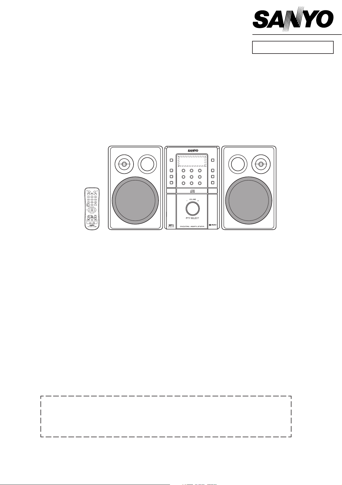
Service Manual
Micro Component System
DC-MP7500(BK)
DC-MP7500(SL)
(XE)
(XE)
PRODUCT CODE No.
129 686 50 (BK)
129 686 55 (SL)
Laser beam safety precaution .......................................... 1
Tape adjustments ............................................................ 1
Tuner adjustments ........................................................... 2
CD pick-up maintenance .................................................. 2
Exploded view .................................................................. 3
Parts list ........................................................................... 4
Exploded view & Parts list
(CD mechanism) ........................................................... 9
IC block diagram & description ........................................ 10
FL display description ...................................................... 19
Wiring connection ............................................................ 20
Schematic diagram
(FRONT) ....................................................................... 22
(CD) ............................................................................... 24
This service manual consists of
For BK ; "DC-MP7500U(BK)/XE" (Main unit : 129 685 50), " SX-MP7500L(BK)/XE" (Speaker system(left):
165 098 03) & "SX-MP7500R(BK)/XE" (Speaker system(right) : 165 106 03)
For SL ; "DC-MP7500U(SL)/XE" (Main unit : 129 685 55), " SX-MM7000L/XE" (Speaker system(left) :
165 098 01) & "SX-MM7000R/XE" (Speaker system(right) : 165 106 01).
(AMPLIFIER & MCU) .................................................... 28
(TUNER) ....................................................................... 32
(D-AMP) ........................................................................ 36
Wiring diagram
(VOLUME)..................................................................... 21
(FRONT) ....................................................................... 21
(CD) Parts side view ....................................................26
Pattern side view ................................................. 27
(AMPLIFIER & MCU) .................................................... 30
(TUNER) ....................................................................... 34
(POWER TRANSFORMER) ......................................... 35
(D-AMP) Parts side view ............................................. 37
Pattern side view ..........................................38
(D-AMP POWER SUPPLY) .......................................... 39
REFERENCE No.
SM5810593
Page 2
LASER BEAM SAFETY PRECAUTION
• Pick-up that emits a laser beam is used in this CD player section.
CAUTION :
THIS PRODUCT CONTAINS A LOW
POWER LASER DEVICE, TO
ENSURE CONTINUED SAFETY DO
NOT REMOVE ANY COVERS OR
ATTEMPT TO GAIN ACCESS TO THE
INSIDE OF THE PRODUCT. REFER
ALL SERVICING TO QUALIFIED
PERSONNEL.
LASER OUTPUT .............. 0.6 mW Max.
CW)
WAVELENGTH .................. 790 nm
TAPE ADJUSTMENTS
1. Azimuth Adjustment
• Be sure to clean the heads before attempting to make any adjustment.
• Be sure both channels (1 and 2) are the same level.
(Using a dual-channel oscilloscope)
• Be sure both channel's waveform are same for the phase matching.
• After completion of the adjustment, use the threadlock (TB-1401B) to
secure the azimuth adjustment screws.
1. Remove the cover deck as Fig.1.
2. Load a test tape (VTT-738 etc. : 10kHz) in the Deck.
NORMAL
3. Press the PLAY button. (Normal playback)
4. Use a + tip screwdriver to turn the screw for normal azimuth
adjustment so that the left and right outputs are maximized at
the same phase during normal playback. See Fig.2.
5. Adjust so that the waveforms for the left and right channels are in alignment.
2. Tape Speed Adjustment
• Connect the Frequency Counter to TAPE OUT.
MOTOR
hole for adjustment
1. Insert the test tape (MTT-111N, etc.; 3,000Hz) into the DECK.
2. Press the PLAY button. .
3. Adjust a hole on the motor bottom so that a frequency counter reading of 3,000 }5Hz is obtained.See Fig.3.
4. Press the STOP button, and eject the test tape.
3. Torque Measurement
Fig.1
Fig.2
Fig.3
- 1 -
Page 3
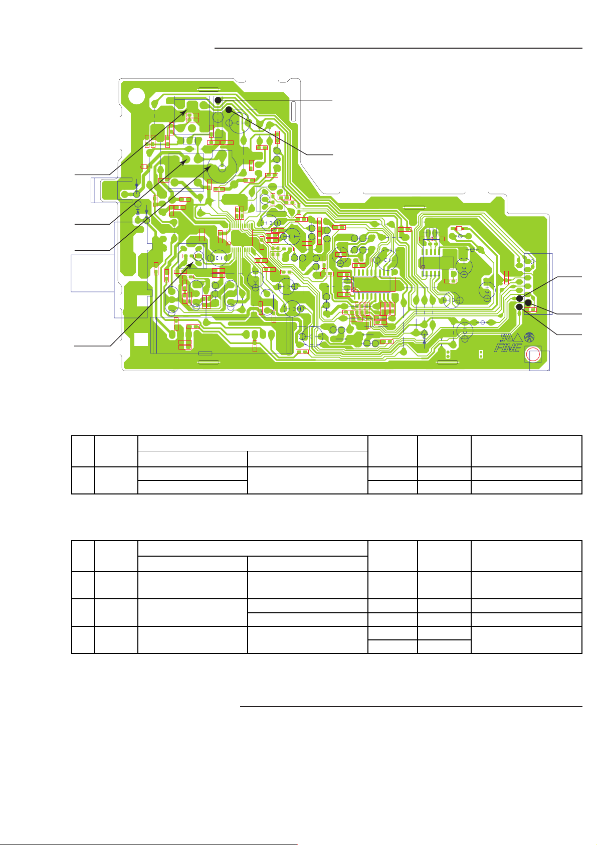
TUNER ADJUSTMENTS
R2108
C2407
R2601
R2602
R2603
R2605
R2604
R2513
C2414
R2104
R2103
C2109
R2606
C2802
C2903
C2902
R2408
C2409
L2353
R2328
C2325
J2101
C2320
D2330
C2321
R2322
R2321
J2002
J2104
L2353
L2351
CT252
T2001
D2103
D2102
CN203
D2100
D2101
CN201
J2106
CAN
CAN
R2001
L2351
CAN
CAN
J2010
C2413
C2411
XF221
CAN
T2001
R2103
R2103
CAN
CAN CAN
R2108
R2108
R2003
C2004
C2002
R2002
J2006
XF220
C2329
R2330
CT252
CAN
J2005
R2053
C2107
R2102
R2101
R2104
R2104
Q2101
J2109
VT
C2317
CAN
J2102
C2412
IC211
C2436
C2104
J2203
E
XF222
U2001
J2103
J2105
CAN
C2425
R2401
C2402
J2014
CAN
J2003
C2201
C2106
J2015
J2201
CAN
R2426
T2405
C2406
R2403
C2430
C2213
C2414
C2414
CAN
J2001
R2430
R2408
R2408
C2404
C2407
C2407
R2417
R2420
C2419
R2429
C2222
X2107
C2109
C2109
E
Q2427
C2409
C2409
Q2418
CAN
C2907
J2009
C2405
C2211
J2110
C2410
TP5
TP6
E
CAN
J2012
E
J2107
C2805
J2210
Q2413
R2431
R2414
E
R2422
Q2421
X2503
J2013
Q2802
Q2415
E
C2512
C2423
E
J2201
R2416
C2327
CAN
C2501
C2502
J2108
J2206
E
Q2803
R2803
E
Q2509
E
Q2510
R2513C2511
R2513
R2521
R2802
R2604
R2604
R2801
Q2804
J2008
IC222
R2601
R2602
R2603
R2601
R2602
R2603
R2606
R2606
R2607
R2605
R2605
J2111
E
• Use a plastic screw driver for adjustments.
• MODE : ST (Stereo)
• Speaker impedance : 6 ohms
• TUNING
FM : 87.5 - 108MHz
AM : 522 - 1611kHz (9kHz steps)
520-1610kHz (10kHz steps)
J2007
X2901
J2202
C2518
R2608
R2709
R2609
R2610
R2316
C2519
J2205
C2903C2902
C2903
J2204
J2112
C2902
IC223
J2208
J2209
J2016
D2709
C2908
D2901
J2207
L2902
L2901
C2906
C2904
C2905
L2801
C2003
RDS_DA
RDS_CLK
PLL_DA
PLL_CLK
PLL_PRI
CN231
ST
GND
+5.6V
C2801
+8.5V
TU_L
GND
C2802
C2802
TU_R
1AD4B10D2520C
T002A 94V-0
TP9
TP8
TP7
1. FM
Step
2
2. AM
Step
1
2
Adjusting
Circuit
Cover
Voltage
Adjusting
Circuit
IF
Adjustment
Cover
Voltage
Antenna : 75Ω unbalanced, Modulation : 1 kHz
Dev. : 22.5kHz(MONO), 22.5kHz(STEREO),6.75kHz(PILOT)
RF Level : dBuV EMF
Output Level : about 30mV at TP13, TP14, TP15
Connection
Input Output
--- TP5 (H) 87.5MHz -- - 1.37±0.50V Check Only
--- TP6 (E) 108.0MHz --- 6.80±0.50V Check Only
SG
Frequency
Adjustment
Remark
Anntena : IRE Loop(SG), Moduration : 1kHz 30%
RF Level : dBuV EMF
Output Level : about 30mV at TP13, TP14, TP15
Input
Loop Ant
---
Connection
Output
---
TP5(H ) 522kHz
TP6(E) 1611kHz --- 7.20±0.50V Check Only
TP9 (L),TP7 (R) ,TP8 (E)3 Tracking Loop Ant
SG
Frequency
450KHz
at 999kHz
Adjustment
T2001
L2353
603kHz L2351
1404kHz CT252
Remark
Maximum
1.00±0.05V
Maximum
CD PICK-UP MAINTENANCE
About pick-up (Optical lens) Cleaning
Clean a lens with swab of the cotton which moistened it with alcohol, cleaning paper or cleaning disc appointed.
Specified cleaning disc : LC-1 (Part code : 645 026 1961 ..... manufactured by SANYO.)
Show a clean procedure in the following in reference by swab of cotton.
1. Cotton swab is wrapped with Cleaning paper.
2. Add the isopropyl alcohol.
3. Gently move the tip of cotton swab just like a draw a whirlpool from inside to outside on the surface of lens.
- 2 -
Page 4
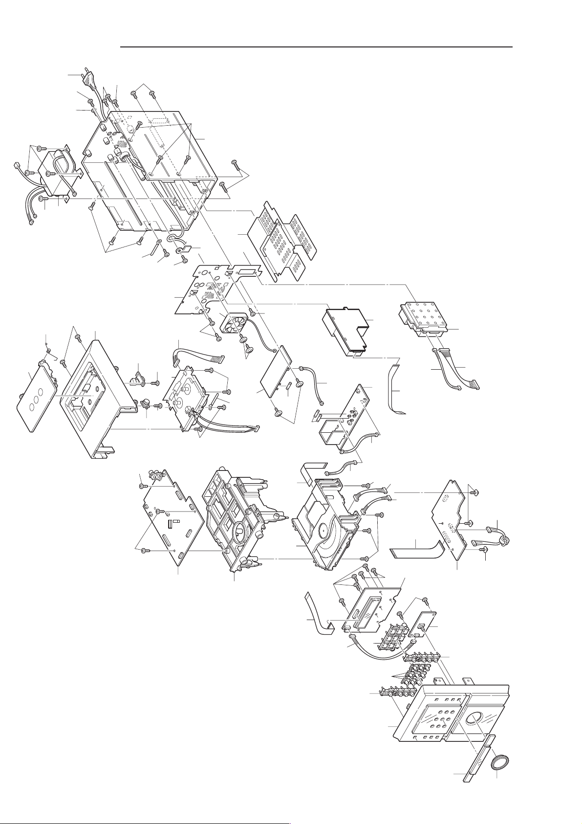
EXPLODED VIEW
6
Y03
Y02
Y04
Y04
Y01
Y02
Y03
3
15
14
13
16
N.S.P
77
78
Y06
Y14
Y15
Y16
Y18
Y12
Y18
Y19
Y19
Y20
Y20
Y20
Y16
Y17
2
4
4
5
8
7
72
73
74
65
64
76
75
57
17
71
9
10
11
12
Y06
Y09
Y10
Y11
Y05
Y05
Y09
Y08
Y13
Y14
Y07
55
62
67
52
51
63
60
61
66
68
69
56
58
59
54
53
This is a basic exploded view.
- 3 -
Page 5

PARTS LIST
PRODUCT SAFETY NOTICE
EACH PRECAUTION IN THIS MANUAL SHOULD BE FOLLOWED DURING SERVICING. COMPONENTS IDENTIFIED WITH THE
!!
IEC SYMBOL
PERFORMANCE CAN BE OF SPECIAL SIGNIFICANCE. WHEN REPLACING A COMPONENT IDENTIFIED BY
REPLACEMENT PARTS DESIGNATED, OR PARTS WITH THE SAME RATINGS OF RESISTANCE, WATTAGE OR VOLTAGE THAT
ARE DESIGNATED IN THE PARTS LIST IN THIS MANUAL. LEAKAGE-CURRENT OR RESISTANCE MEASUREMENTS MUST BE
MADE TO DETERMINE THAT EXPOSED PARTS ARE ACCEPTABLY INSULATED FROM THE SUPPLY CIRCUIT BEFORE
RETURNING THE PRODUCT TO THE CUSTOMER.
CAUTION : Regular type resistors and capacitors are not listed. To know those values, refer to the schematic diagram.
N.S.P : Not available as service parts.
!
IN THE PARTS LIST AND THE SCHEMATIC DIAGRAM DESIGNATED COMPONENTS IN WHICH SAFETY AND
!!
!
, USE ONLY THE
Regular type resistors are less than 1/4 W carbon type and 0 ohm chip resistors.
Regular type capacitors are less than 50 V and less than 1000 µF type of Ceramic type and Electrical type.
PACKING & ACCESSORIES
REF.NO. PART NO. DESCRIPTION
614 330 1905 CARTON CASE(For BK)
614 330 9413 CARTON CASE(For SL)
614 329 8342 CUSHION,FRONT
614 329 8359 CUSHION,REAR
614 330 1400 INSTRUCTION MANUAL(For BK)
614 330 9475 INSTRUCTION MANUAL(For SL)
614 330 7136 INSTRUCTION SHEET(For BK)
614 330 9505 INSTRUCTION SHEET(For SL)
614 229 4635 ANT
614 308 5515 ANT
645 063 7483 ASSY,ANTENA,LOOP
614 330 8874 LID,BATTERY REMOCON
645 067 1494 REMOCON,RB-MCR350MO
614 330 6009 ASSY,BOX,SPEAKER(For BK)
614 330 1462 ASSY,BOX,SPEAKER(For SL)
CABINET & CHASSIS
REF.NO. PART NO. DESCRIPTION
1 614 330 9024 ASSY,KNOB,VOLUME
2 614 330 9338 ASSY,COVER,CD,DOOR(For BK)
2 614 330 9017 ASSY,COVER,CD,DOOR(For SL)
3 614 330 1240 ASSY,PANEL FRONT(For BK)
3 614 331 0037 ASSY,PANEL FRONT(For SL)
4 614 329 1855 BUTTON,OPERATION
5 614 329 1848 BUTTON,OPERATION
6 614 329 1930 DEC,BUTTON
7 614 329 1985 MOUNTING,CD
8 614 322 2132 ASSY,GEAR,LID,CASSETTE
9 614 329 6737 LATCH,CAM
10 614 330 6283 PANEL,TOP(For BK)
10 614 329 2012 PANEL,TOP(For SL)
11 614 329 2067 SPRING,DOOR DEC
12 614 330 6221 LID,CASSETTE(For BK)
12 614 329 1978 LID,CASSETTE(For SL)
13 614 330 1509 PANEL,REAR
14 614 329 1862 CABINET,BOTTOM
15 614 330 1233 ASSY,CABINET,REAR(For BK)
15 614 331 0853 ASSY,CABINET,REAR(For SL)
REF.NO. PART NO. DESCRIPTION
Y08 412 032 6408 SPECIAL SCREW,
CABINET RAER+FAN
Y09 411 021 3503 SCR S-TPG BIN 3X10,
PANEL TOP+CASSETTE MECHA
Y10 411 021 3503 SCR S-TPG BIN 3X10,
PANEL TOP+ASSY GEAR
Y11 411 021 3503 SCR S-TPG BIN 3X10,
PANEL TOP+LATCH CAM
Y12 411 021 3701 SCR S-TPG BIN 3X10,(For BK)
CABINET REAR+PANEL TOP
Y12 411 021 3404 SCR S-TPG BIN 3X10,(For SL)
CABINET REAR+PANEL TOP
Y13 411 021 3503 SCR S-TPG BIN 3X10,
PANEL REAR+CABINET REAR
Y14 411 021 3503 SCR S-TPG BIN 3X10,
POWER AC CORD
Y15 411 021 3503 SCR S-TPG BIN 3X10,
CABINET REAR+FAN
Y16 411 022 2901 SCR S-TPG FLT 3X10,(For BK)
PANEL FRONT+PANET TOP+CA,
CABINETL RAER+PANEL FRONT,
CABINET RAER+PANEL TOP
Y16 411 098 7701 SCR S-TPG FLT 3X10,(For SL)
PANEL FRONT+PANET TOP+CA,
CABINETL RAER+PANEL FRONT,
CABINET RAER+PANEL TOP
Y17 411 021 4906 SCR S-TPG BIN 3X20,
PANEL FRONT+CABINET REAR
Y18 411 021 8300 SCR S-TPG BIN 4X16,
CABINET REAR+TRANS
Y19 411 021 3503 SCR S-TPG BIN 3X10,
CABINET REAR+D-AMP,TUNER
Y20 411 021 3701 SCR S-TPG BIN 3X10,(For BK)
CABINET REAR+(SPK SOCKET,
MOUNTING CD,VIDEO IN,
FM SOCKET)
Y20 411 021 3404 SCR S-TPG BIN 3X10,(For SL)
CABINET REAR+(SPK SOCKET,
MOUNTING CD,VIDEO IN,
FM SOCKET)
FIXING PARTS
REF.NO. PART NO. DESCRIPTION
Y01 411 021 3503 SCR S-TPG BIN 3X10,
PANEL FRONT+VOL PWB
Y02 411 021 3503 SCR S-TPG BIN 3X10,
PANEL FRONT+FRONT PWB
Y03 411 020 9902 SCR S-TPG BRZ+FLG 3X8,CD-PWB
Y04 411 021 3503 SCR S-TPG BIN 3X10,
MOUNTING CD+CD MECHA
Y05 411 021 6405 SCR S-TPG BIN 3X8,
MOUNTING CD+MAIN PWB
Y06 614 129 9136 LUG(FOR C_MECHA,CABINETREAR,
MAIN PWB, ASSY MECHA)
Y07 412 032 6408 SPECIAL SCREW,
CABINET REAR+FAN
ELECTRICAL PARTS
REF.NO. PART NO. DESCRIPTION
51 614 330 9161 ASSY,WIRE,FRONT TO VOL
52 614 330 9253 FLEXIBLE FLAT CABLE,
MAIN TO FRONT
53 614 330 9239 FLEXIBLE FLAT CABLE,MAIN TO CD
54 614 330 9147 ASSY,WIRE,MAIN TO CD
55 614 326 3739 ASSY,WIRE,ASSY WIRE
56 614 326 3722 ASSY,WIRE,ASSY WIRE
57 614 327 0850 FLEXIBLE FLAT CABLE,FFC
or 614 326 3647 FLEXIBLE FLAT CABLE,FFC
58 614 330 9123 ASSY,WIRE,DAMP DG TO CD
59 614 330 9208 ASSY,WIRE,FRONT TO DAMP DG
60 614 330 9192 ASSY,WIRE,MAIN TO DAMP
- 4 -
Page 6

PARTS LIST
REF.NO. PART NO. DESCRIPTION
61 614 330 9130 ASSY,WIRE,DAMP DG TO DAMP
62 614 330 9246 FLEXIBLE FLAT CABLE,MAIN TO TU
63 614 330 9116 ASSY,WIRE,MAIN TO AC DG
64 423 016 9902 FUSE 250V 0.8A
65 423 016 8103 FUSE 250V 4A
or 423 016 8103 FUSE 250V 4A
66 614 330 9178 ASSY,WIRE,MAIN TO TAPE
67 645 068 8034 MOTOR,FAN DC 0.84W
68 645 067 1975 TRANS,POWER
69 645 016 9939 CORD,POWER-1.74MK
VOLUME P.W.BOARD ASSY
REF.NO. PART NO. DESCRIPTION
71 614 329 8663 ASSY,PWB,VOL(Only initial)
CN630 645 006 0939 PLUG,6P,FRONT-VOL
or 614 310 2625 PLUG,6P,FRONT-VOL
D6301 407 239 4104 LED LT5C31-81-UR91,VOL-LED
D6302 407 239 4104 LED LT5C31-81-UR91,VOL-LED
D6303 407 239 4203 LED LT5CB1-81-URE3,VOL-LED
D6304 407 239 4203 LED LT5CB1-81-URE3,VOL-LED
D6305 407 012 4406 DIODE 1SS133
Q6301 405 143 0007 TR KRC107M
or 405 000 3806 TR DTC114YS
Q6305 405 000 3806 TR DTC114YS
or 405 143 0007 TR KRC107M
S6301 645 068 3022 SWITCH,ROTARY(ENCODER)
FRONT P.W.BOARD ASSY
REF.NO. PART NO. DESCRIPTION
72 614 329 8625 ASSY,PWB,FRONT(Only initial)
BR601 614 325 4249 HOLDER,FL
CN602 645 011 9972 SOCKET,FPC 11P,FRONT-MAIN
or 645 009 4156 SOCKET,FFC 11P,FRONT-MAIN
CN603 614 310 2625 PLUG,6P,FRONT-VOL
or 645 006 0939 PLUG,6P,FRONT-VOL
D6001 407 012 4406 DIODE 1SS133
D6002 407 012 4406 DIODE 1SS133
D6003 407 012 4406 DIODE 1SS133
D6004 407 012 4406 DIODE 1SS133
D6005 407 099 5204 ZENER DIODE MTZJ5.1B
D6006 407 099 9509 ZENER DIODE MTZJ30B
D6101 407 012 4406 DIODE 1SS133
D6201 407 012 4406 DIODE 1SS133
D6202 407 231 3808 LED LT2P11-81,STAND-BY-LED
FL601 645 067 8295 FLOURESCENT TUBE,FL
IC601 409 519 6907 IC PT6315
L6201 645 001 5441 INDUCTOR,2.2U K
Q6201 405 000 3806 TR DTC114YS
or 405 143 0007 TR KRC107M
Q6202 405 000 3806 TR DTC114YS
or 405 143 0007 TR KRC107M
R6002 402 083 7707 RESISTOR 1K J- 1W
S6150 614 220 5471 SWITCH,TACT
or 614 240 1002 SWITCH,TACT
or 645 006 5958 SWITCH,PUSH 1P-1T
S6151 614 220 5471 SWITCH,TACT
or 614 240 1002 SWITCH,TACT
or 645 006 5958 SWITCH,PUSH 1P-1T
S6152 645 006 5958 SWITCH,PUSH 1P-1T
or 614 240 1002 SWITCH,TACT
or 614 220 5471 SWITCH,TACT
S6153 645 006 5958 SWITCH,PUSH 1P-1T
or 614 240 1002 SWITCH,TACT
or 614 220 5471 SWITCH,TACT
S6154 645 006 5958 SWITCH,PUSH 1P-1T
or 614 240 1002 SWITCH,TACT
or 614 220 5471 SWITCH,TACT
S6155 614 220 5471 SWITCH,TACT
or 614 240 1002 SWITCH,TACT
or 645 006 5958 SWITCH,PUSH 1P-1T
REF.NO. PART NO. DESCRIPTION
S6156 645 006 5958 SWITCH,PUSH 1P-1T
or 614 240 1002 SWITCH,TACT
or 614 220 5471 SWITCH,TACT
S6157 645 006 5958 SWITCH,PUSH 1P-1T
or 614 240 1002 SWITCH,TACT
or 614 220 5471 SWITCH,TACT
S6158 645 006 5958 SWITCH,PUSH 1P-1T
or 614 240 1002 SWITCH,TACT
or 614 220 5471 SWITCH,TACT
S6160 645 006 5958 SWITCH,PUSH 1P-1T
or 614 240 1002 SWITCH,TACT
or 614 220 5471 SWITCH,TACT
S6161 614 220 5471 SWITCH,TACT
or 614 240 1002 SWITCH,TACT
or 645 006 5958 SWITCH,PUSH 1P-1T
S6162 614 220 5471 SWITCH,TACT
or 614 240 1002 SWITCH,TACT
or 645 006 5958 SWITCH,PUSH 1P-1T
S6163 614 220 5471 SWITCH,TACT
or 614 240 1002 SWITCH,TACT
or 645 006 5958 SWITCH,PUSH 1P-1T
S6164 614 220 5471 SWITCH,TACT
or 645 006 5958 SWITCH,PUSH 1P-1T
or 614 240 1002 SWITCH,TACT
S6165 645 006 5958 SWITCH,PUSH 1P-1T
or 614 240 1002 SWITCH,TACT
or 614 220 5471 SWITCH,TACT
S6166 645 006 5958 SWITCH,PUSH 1P-1T
or 614 240 1002 SWITCH,TACT
or 614 220 5471 SWITCH,TACT
S6167 614 220 5471 SWITCH,TACT
or 614 240 1002 SWITCH,TACT
or 645 006 5958 SWITCH,PUSH 1P-1T
SE601 407 217 1101 PHOTO DIODE SPS-442-1G
or 407 229 6101 PHOTO DIODE SPS-442-1-G1
CD P.W.BOARD ASSY
REF.NO. PART NO. DESCRIPTION
73 614 329 8731 ASSY,PWB,CD(Only initial)
CN111 645 042 5349 SOCKET,FPC 16P
CN113 645 006 0939 PLUG,6P
or 614 310 2625 PLUG,6P
CN114 614 310 2618 PLUG,5P
or 645 006 0922 PLUG,5P
CN130 645 012 5591 SOCKET,FPC 26P
or 645 059 6582 SOCKET,FFC 26P
CN140 614 310 2465 PLUG,5P
or 645 005 9292 PLUG,5P
CN142 614 310 2441 PLUG,3P
or 645 005 7373 PLUG,3P
CN180 645 060 2085 SOCKET,IC 32P(IC180)
D1011 407 177 5300 DIODE RL153-M13
D1012 407 177 5300 DIODE RL153-M13
D1530 407 099 5105 ZENER DIODE MTZJ4.7B
D1601 407 012 4406 DIODE 1SS133
or 407 012 5809 DIODE 1SS176
D1602 407 012 4406 DIODE 1SS133
or 407 012 5809 DIODE 1SS176
D1603 407 012 4406 DIODE 1SS133
or 407 012 5809 DIODE 1SS176
D1641 407 127 3806 ZENER DIODE MTZJ3.3B
D1642 407 148 6701 DIODE 1A3-I
D1643 407 148 6701 DIODE 1A3-I
D1651 407 127 3806 ZENER DIODE MTZJ3.3B
D1652 407 148 6701 DIODE 1A3-I
D1653 407 148 6701 DIODE 1A3-I
D1661 407 099 4603 ZENER DIODE MTZJ3.9B
IC110 410 468 0205 IC TA2153FN,RFAMP
IC120 410 468 0304 IC TC9462F,CDDSP
IC121 410 472 2509 IC TC74HC14AFN-EL,HEXINVERTER
IC122 409 051 2702 IC TC4052BF,ANALOGSW
IC130 410 468 0403 IC TA2092N,SERVODRIVER
- 5 -
Page 7

PARTS LIST
REF.NO. PART NO. DESCRIPTION REF.NO. PART NO. DESCRIPTION
IC140 410 468 0502 IC TC74HCU04AFN-EL,
HEXINVERTER
IC150 409 408 1303 IC LB1641L
IC160 409 574 9509 IC ES3890F,VCDPROCESSOR
IC170 409 573 2808 IC PT8211S,DAC
IC180 410 497 9705 IC ASSY,EPROM4M
(IC MX29F004TPC-70)
IC190 410 499 1905 IC M11L16161SA-45T,DRAM16M
or 410 505 2100 IC MSM51V18165F-60TS-K,
DRAM16M
L1010 645 006 3886 INDUCTOR,1U K
L1131 645 001 5519 INDUCTOR,47U K
L1132 645 001 4550 INDUCTOR,10U K
L1280 645 001 4581 INDUCTOR,100U K
L1601 645 001 5465 INDUCTOR,3.3U K
L1602 645 037 2858 CORE,PIPE
L1603 645 037 2858 CORE,PIPE
L1605 645 034 7887 INDUCTOR,1000 OHM
or 645 045 7869 IMPEDANCE,1000 OHM P
or 645 020 1813 INDUCTOR,1000 OHM
L1606 645 020 1813 INDUCTOR,1000 OHM
or 645 034 7887 INDUCTOR,1000 OHM
or 645 045 7869 IMPEDANCE,1000 OHM P
L1607 645 037 2858 CORE,PIPE
L1701 645 001 4581 INDUCTOR,100U K
Q1131 405 008 6809 TR 2SB808-F-SPA
or 405 008 7202 TR 2SB810-E
or 405 008 7301 TR 2SB810-F
Q1601 405 141 3307 TR KTC3198-GR
or 405 141 3208 TR KTC3198-Y
or 405 019 2708 TR 2SC536-F-NP
or 405 019 3804 TR 2SC536-G-NP
Q1641 405 025 0200 TR 2SD734-G
or 405 141 3109 TR KTC3203-Y
or 405 024 9907 TR 2SD734-F
Q1651 405 141 3109 TR KTC3203-Y
or 405 024 9907 TR 2SD734-F
or 405 025 0200 TR 2SD734-G
Q1661 405 141 3109 TR KTC3203-Y
or 405 024 9907 TR 2SD734-F
or 405 025 0200 TR 2SD734-G
R1530 402 083 3600 RESISTOR 15 J- 2W
X1451 645 059 0948 OSC,CRYSTAL 16.9344MHZ
X1601 645 059 0955 OSC,CRYSTAL 27.000MHZ,27MHZ
AMPLIFIER & MCU P.W.BOARD ASSY
REF.NO. PART NO. DESCRIPTION
74 614 329 8618 ASSY,PWB,AMP-MCU(Only initial)
C4459 403 329 5907 ELECT 3300U M 25V
or 403 366 5601 ELECT 3300U M 25V
C4559 403 389 0805 ELECT 3300U R 16V
C4601 403 057 3503 POLYESTER 0.1U K 50V
C4605 403 061 3605 POLYESTER 0.039U J 50V
C4606 403 061 7702 POLYESTER 4700P J 50V
C4607 403 056 7502 POLYESTER 1000P J 50V
C4608 403 060 2807 POLYESTER 0.027U K 50V
C4727 403 259 0508 NP-ELECT 1U M 50V
C4827 403 259 0508 NP-ELECT 1U M 50V
CN432 614 310 2441 PLUG,3P
or 645 005 7373 PLUG,3P
CN435 614 310 2434 PLUG,2P
or 645 005 7366 PLUG,2P
CN439 614 319 3456 PLUG,3P
or 645 006 1806 PLUG,3P
CN440 614 310 2472 PLUG,6P
or 645 005 8127 PLUG,6P
CN455 614 310 2465 PLUG,5P
or 645 005 9292 PLUG,5P
CN461 614 310 2533 PLUG,12P
or 645 006 0878 PLUG,12P
CN470 614 253 9354 SOCKET,RCA TERMINAL
CN471 614 221 8273 TERMINAL
CN651 645 009 4163 SOCKET,FFC 12P
or 645 012 5096 SOCKET,FPC 12P
CN652 645 005 8141 PLUG,9P
or 614 310 2502 PLUG,9P
CN653 645 009 4156 SOCKET,FFC 11P
or 645 011 9972 SOCKET,FPC 11P
CN654 645 009 8468 SOCKET,FFC 26P
or 645 012 5300 SOCKET,FPC 26P
CN655 614 310 2496 PLUG,8P
or 645 005 8134 PLUG,8P
D4320 407 099 6003 ZENER DIODE MTZJ9.1B
D4330 407 099 6805 ZENER DIODE MTZJ13B
D4331 407 012 4406 DIODE 1SS133
D4332 407 012 4406 DIODE 1SS133
D4340 407 148 6701 DIODE 1A3-I
D4341 407 012 4406 DIODE 1SS133
D4342 407 148 6701 DIODE 1A3-I
D4465 407 148 6701 DIODE 1A3-I
D4466 407 148 6701 DIODE 1A3-I
D4467 407 148 6701 DIODE 1A3-I
D4468 407 148 6701 DIODE 1A3-I
D6501 407 012 4406 DIODE 1SS133
D6502 407 012 4406 DIODE 1SS133
D6503 407 012 4406 DIODE 1SS133
D6504 407 012 4406 DIODE 1SS133
D6701 407 012 4406 DIODE 1SS133
D6702 407 012 4406 DIODE 1SS133
HS430 614 329 1947 HEAT SINK
HS431 614 329 9950 HEAT SINK
IC434 409 463 6701 IC KIA7805API
IC440 409 451 7406 IC AN7348K
IC441 410 468 0809 IC TC9422F
IC443 409 189 3404 IC BA7755A
IC651 410 497 8005 IC TMP87EP26F-4K76,MICON
L4600 645 006 1523 INDUCTOR,470U J
L4601 645 006 1523 INDUCTOR,470U J
L4602 645 037 2858 CORE,PIPE
L4603 645 006 1523 INDUCTOR,470U J
L4604 645 037 2858 CORE,PIPE
L6501 645 001 4581 INDUCTOR,100U K
or 645 031 7842 INDUCTOR,100U K
L6502 645 001 4581 INDUCTOR,100U K
or 645 031 7842 INDUCTOR,100U K
L6503 645 001 4581 INDUCTOR,100U K
or 645 031 7842 INDUCTOR,100U K
PR430 645 042 2676 PROTECTOR,2.5A 125V
PR431 645 027 4169 PROTECTOR,0.125A 125V
PR432 645 042 2614 PROTECTOR,1A 125V
PR433 645 042 2614 PROTECTOR,1A 125V
Q4300 405 146 2206 TR KTC3875-GR
or 405 146 2107 TR KTC3875-Y
or 405 011 1006 TR 2SC1623-L6
or 405 014 4509 TR 2SC2412K-R
Q4301 405 146 2206 TR KTC3875-GR
or 405 146 2107 TR KTC3875-Y
or 405 011 1006 TR 2SC1623-L6
or 405 014 4509 TR 2SC2412K-R
Q4302 405 146 2206 TR KTC3875-GR
or 405 146 2107 TR KTC3875-Y
or 405 011 1006 TR 2SC1623-L6
or 405 014 4509 TR 2SC2412K-R
Q4303 405 014 4509 TR 2SC2412K-R
or 405 011 1006 TR 2SC1623-L6
or 405 146 2107 TR KTC3875-Y
or 405 146 2206 TR KTC3875-GR
Q4320 405 004 5004 TR 2SA608-G-NP
or 405 004 4502 TR 2SA608-F-NP
or 405 141 3505 TR KTA1266-Y
or 405 141 3406 TR KTA1266-GR
Q4321 405 019 2708 TR 2SC536-F-NP
or 405 019 3804 TR 2SC536-G-NP
or 405 141 3208 TR KTC3198-Y
or 405 141 3307 TR KTC3198-GR
- 6 -
Page 8
PARTS LIST
REF.NO. PART NO. DESCRIPTION REF.NO. PART NO. DESCRIPTION
Q4322 405 138 6403 TR KTD2058Y
or 405 095 1602 TR 2SD2061-E
or 405 095 1701 TR 2SD2061-F
Q4330 405 141 3406 TR KTA1266-GR
or 405 141 3505 TR KTA1266-Y
or 405 004 4502 TR 2SA608-F-NP
or 405 004 5004 TR 2SA608-G-NP
Q4331 405 138 6403 TR KTD2058Y
or 405 095 1602 TR 2SD2061-E
or 405 095 1701 TR 2SD2061-F
Q4600 405 008 2504 TR 2SB698-G
or 405 008 2405 TR 2SB698-F
or 405 141 3703 TR KTA1271-Y
Q4601 405 143 0007 TR KRC107M
or 405 000 3806 TR DTC114YS
Q4602 405 141 3208 TR KTC3198-Y
or 405 019 3804 TR 2SC536-G-NP
or 405 019 2708 TR 2SC536-F-NP
or 405 141 3307 TR KTC3198-GR
Q4603 405 019 3804 TR 2SC536-G-NP
or 405 019 2708 TR 2SC536-F-NP
or 405 141 3307 TR KTC3198-GR
or 405 141 3208 TR KTC3198-Y
Q4604 405 143 0007 TR KRC107M
or 405 000 3806 TR DTC114YS
Q4700 405 075 8607 TR DTC143ZS
or 405 143 9000 TR KRC106M
Q4800 405 075 8607 TR DTC143ZS
or 405 143 9000 TR KRC106M
Q6502 405 141 3307 TR KTC3198-GR
or 405 141 3208 TR KTC3198-Y
or 405 019 2708 TR 2SC536-F-NP
or 405 019 3804 TR 2SC536-G-NP
Q6701 405 155 0002 TR MPSA56
Q6702 405 155 0002 TR MPSA56
Q6703 405 155 0002 TR MPSA56
Q6704 405 143 0007 TR KRC107M
or 405 000 3806 TR DTC114YS
Q6705 405 143 0007 TR KRC107M
or 405 000 3806 TR DTC114YS
SA430 411 021 6405 SCR S-TPG BIN 3X8
SA431 411 021 6405 SCR S-TPG BIN 3X8
SA432 411 021 6405 SCR S-TPG BIN 3X8
SA433 411 021 6405 SCR S-TPG BIN 3X8
SA434 411 021 6405 SCR S-TPG BIN 3X8
X6501 645 063 9791 OSC,CRYSTAL 7.372800MHZ
X6502 645 032 1627 OSC,CRYSTAL 32.768KHZ
D-AMP POWER SUPPLY P.W.BOARD ASSY
REF.NO. PART NO. DESCRIPTION
75 614 329 8656 ASSY,PWB,D-AMP(Only initial)
C4104 403 325 2306 ELECT 4700U M 35V
C4105 403 325 2306 ELECT 4700U M 35V
C4110 403 325 1705 ELECT 4700U M 16V
or 403 329 5709 ELECT 4700U M 16V
or 413 134 5604 ELECT 4700U M 16V
CN410 645 005 7373 PLUG,3P
or 614 310 2441 PLUG,3P
CN411 645 006 1806 PLUG,3P
CN412 645 006 1806 PLUG,3P
or 614 319 3456 PLUG,3P
CN413 645 031 7903 HOLDER,FUSE
or 645 006 4760 HOLDER,FUSE
CN414 645 031 7903 HOLDER,FUSE
or 645 006 4760 HOLDER,FUSE
CN415 645 031 7903 HOLDER,FUSE
or 645 006 4760 HOLDER,FUSE
CN416 645 031 7903 HOLDER,FUSE
or 645 006 4760 HOLDER,FUSE
CN417 645 006 1813 PLUG,4P
CN418 645 005 7373 PLUG,3P
or 614 310 2441 PLUG,3P
D4100 407 196 5800 DIODE 1N5402BD82
D4101 407 196 5800 DIODE 1N5402BD82
D4102 407 196 5800 DIODE 1N5402BD82
D4103 407 196 5800 DIODE 1N5402BD82
D4104 407 098 3300 DIODE RL153-BF-S2
D4106 407 196 5800 DIODE 1N5402BD82
D4107 407 196 5800 DIODE 1N5402BD82
D4108 407 196 5800 DIODE 1N5402BD82
D4109 407 196 5800 DIODE 1N5402BD82
D4110 407 099 5204 ZENER DIODE MTZJ5.1B
D4111 407 012 4406 DIODE 1SS133
JW601 645 069 0143 CORD,SOCKET,ASSY WIRE
PR410 645 042 2614 PROTECTOR,1A 125V
PR411 645 042 2676 PROTECTOR,2.5A 125V
PR414 645 042 2560 PROTECTOR,0.75A 125V
Q4100 405 141 3406 TR KTA1266-GR
or 405 141 3505 TR KTA1266-Y
or 405 004 4502 TR 2SA608-F-NP
or 405 004 5004 TR 2SA608-G-NP
Q4101 405 138 6403 TR KTD2058Y
or 405 095 1701 TR 2SD2061-F
or 405 095 1602 TR 2SD2061-E
Q4102 405 141 3307 TR KTC3198-GR
or 405 019 2708 TR 2SC536-F-NP
or 405 019 3804 TR 2SC536-G-NP
or 405 141 3208 TR KTC3198-Y
R4130 401 120 1500 MT-FILM 10 FD 1/4W
SA410 411 021 6405 SCR S-TPG BIN 3X8
POWER TRANSFORMER P.W.BOARD ASSY
REF.NO. PART NO. DESCRIPTION
76 614 329 8649 ASSY,PWB,DG(Only initial)
C4008 403 349 3303 CERAMIC 0.01U M 250V
or 403 366 7803 CERAMIC 0.01U M 250V
CN400 645 005 9315 PLUG,2P
CN401 614 017 8203 TERMINAL BOARD
CN402 614 017 8203 TERMINAL BOARD
CN403 645 006 4760 HOLDER,FUSE
or 645 031 7903 HOLDER,FUSE
CN404 645 006 4760 HOLDER,FUSE
or 645 031 7903 HOLDER,FUSE
CN405 614 310 2441 PLUG,3P
or 645 005 7373 PLUG,3P
D4001 407 012 4406 DIODE 1SS133
D4002 407 099 5402 ZENER DIODE MTZJ6.2B
D4004 407 097 8009 DIODE MPG06G
D4005 407 097 8009 DIODE MPG06G
D4006 407 097 8009 DIODE MPG06G
D4007 407 097 8009 DIODE MPG06G
L4001 645 038 7364 INDUCTOR,70U
PT410 645 067 6178 TRANS,POWER
Q4001 405 141 3208 TR KTC3198-Y
or 405 141 3307 TR KTC3198-GR
or 405 019 2708 TR 2SC536-F-NP
or 405 019 3804 TR 2SC536-G-NP
Q4002 405 141 1402 TR KTD863-GR
or 405 023 5306 TR 2SD400-F-MP
or 405 023 5009 TR 2SD400-E-MP
RY407 645 030 5597 RELAY
TUNER P.W.BOARD ASSY
REF.NO. PART NO. DESCRIPTION
77 614 329 8632 ASSY,PWB,TUNER(Only initial)
CN201 645 057 1909 TUNER,FM-TERMINAL_XE
CN203 645 004 2683 PLUG,2P,AM-TERMARINL
CN231 645 067 2514 SOCKET,FFC 12P,TU-MAIN
or 645 012 5164 SOCKET,FPC 12P,TU-MAIN
CT252 645 032 5663 TRIMMER,7PF
D2100 407 012 4406 DIODE 1SS133
- 7 -
Page 9

PARTS LIST
REF.NO. PART NO. DESCRIPTION REF.NO. PART NO. DESCRIPTION
D2101 407 012 4406 DIODE 1SS133
D2102 407 012 4406 DIODE 1SS133
D2103 407 149 0807 DIODE 1SS355
D2330 407 105 1602 VARACTOR DI SVC342M-V
or 407 105 1305 VARACTOR DI SVC342L-V
D2709 407 099 4801 ZENER DIODE MTZJ4.3B
D2901 407 149 0807 DIODE 1SS355
IC211 410 468 0601 IC TA2149BFN
IC222 410 468 0700 IC TC9257F
IC223 409 486 0007 IC BU1924F,RDS
L2351 645 037 2377 TRANS,ANT,796KHZ
L2353 645 040 2739 TRANS,OSC,796KHZ
L2801 645 001 4581 INDUCTOR,100U K
or 645 031 7842 INDUCTOR,100U K
L2901 645 031 7835 INDUCTOR,10U K
or 645 001 4550 INDUCTOR,10U K
L2902 645 031 7835 INDUCTOR,10U K
or 645 001 4550 INDUCTOR,10U K
Q2101 405 151 4806 TR KTC3195-O
or 405 151 4301 TR KTC3195-Y
Q2413 405 151 4301 TR KTC3195-Y
or 405 151 4806 TR KTC3195-O
Q2415 405 151 4301 TR KTC3195-Y
or 405 151 4806 TR KTC3195-O
Q2418 405 151 4301 TR KTC3195-Y
or 405 151 4806 TR KTC3195-O
Q2421 405 151 4301 TR KTC3195-Y
or 405 151 4806 TR KTC3195-O
Q2427 405 151 4806 TR KTC3195-O
or 405 151 4301 TR KTC3195-Y
Q2509 405 151 4301 TR KTC3195-Y
or 405 151 4806 TR KTC3195-O
Q2510 405 151 4301 TR KTC3195-Y
or 405 151 4806 TR KTC3195-O
Q2802 405 143 0007 TR KRC107M
or 405 000 3806 TR DTC114YS
Q2803 405 019 3804 TR 2SC536-G-NP
or 405 019 2708 TR 2SC536-F-NP
or 405 141 3208 TR KTC3198-Y
or 405 141 3307 TR KTC3198-GR
Q2804 405 019 3804 TR 2SC536-G-NP
or 405 019 2708 TR 2SC536-F-NP
or 405 141 3208 TR KTC3198-Y
or 405 141 3307 TR KTC3198-GR
T2001 645 043 0213 FILTER,450KHZ
U2001 645 043 6697 TUNER,FM
X2107 645 061 3449 CERAMIC FILTER 10.7MHZ
X2503 645 023 4965 OSC,CRYSTAL 7.2MHZ
X2901 645 035 8326 OSC,CRYSTAL 4.332MHZ
XF220 645 054 1223 CERAMIC FILTER 10.70MHZ
or 645 010 7665 CERAMIC FILTER 10.70MHZ
or 614 240 2917 FILTER,CERAM
XF221 645 059 0054 CERAMIC FILTER 450KHZ
or 645 041 9324 CERAMIC FILTER 450KHZ
XF222 645 054 1223 CERAMIC FILTER 10.70MHZ
or 645 010 7665 CERAMIC FILTER 10.70MHZ
or 614 240 2917 FILTER,CERAM
CN567 645 031 4308 JACK,PHONE D3.6,HEADPHONE
CN587 645 008 5314 TERMINAL,SPEAKER
or 645 064 8519 TERMINAL,SPEAKER 4P
CN597 614 310 2687 PLUG,12P
or 645 006 0991 PLUG,12P
CN599 645 006 1882 PLUG,3P
D5970 407 012 4406 DIODE 1SS133
D5971 407 012 4406 DIODE 1SS133
D5972 407 012 4406 DIODE 1SS133
D5973 407 012 4406 DIODE 1SS133
HS501 614 328 2662 HEAT SINK,D-AMP
IC597 409 568 1502 IC TDA8921TH
L5775 645 063 4017 INDUCTOR,33U K
L5776 645 001 4550 INDUCTOR,10U K
or 645 031 7835 INDUCTOR,10U K
L5875 645 063 4017 INDUCTOR,33U K
L5876 645 001 4550 INDUCTOR,10U K
or 645 031 7835 INDUCTOR,10U K
L5970 645 037 2858 CORE,PIPE
L5971 645 037 2858 CORE,PIPE
L5973 645 037 2858 CORE,PIPE
L5974 645 037 2858 CORE,PIPE
Q5972 405 019 3804 TR 2SC536-G-NP
or 405 019 2708 TR 2SC536-F-NP
or 405 141 3208 TR KTC3198-Y
or 405 141 3307 TR KTC3198-GR
Q5974 405 141 3307 TR KTC3198-GR
or 405 141 3208 TR KTC3198-Y
or 405 019 2708 TR 2SC536-F-NP
or 405 019 3804 TR 2SC536-G-NP
Q5975 405 141 3208 TR KTC3198-Y
or 405 141 3307 TR KTC3198-GR
or 405 019 2708 TR 2SC536-F-NP
or 405 019 3804 TR 2SC536-G-NP
Q5977 405 141 3307 TR KTC3198-GR
or 405 141 3208 TR KTC3198-Y
Q5978 405 141 3307 TR KTC3198-GR
or 405 141 3208 TR KTC3198-Y
or 405 019 2708 TR 2SC536-F-NP
or 405 019 3804 TR 2SC536-G-NP
R5777 402 082 1102 FUSIBLE RES 22 JA 1/2W
R5779 401 009 5605 CARBON 330 JA 1/2W
or 401 009 5803 CARBON 330 JA 1/2W
R5780 401 314 1309 MT-FILM 4.7 FD 1/4W
R5877 402 082 1102 FUSIBLE RES 22 JA 1/2W
R5879 401 009 5605 CARBON 330 JA 1/2W
or 401 009 5803 CARBON 330 JA 1/2W
R5880 401 314 1309 MT-FILM 4.7 FD 1/4W
S5970 614 224 4531 RELAY
S5971 645 059 0306 RELAY
or 645 030 5597 RELAY
SA511 411 021 6405 SCR S-TPG BIN 3X8,FOR SH401
SA512 411 021 6405 SCR S-TPG BIN 3X8,FOR SH401
SA513 411 021 6405 SCR S-TPG BIN 3X8,FOR SH401
SA514 411 021 4005 SCR S-TPG BIN 3X12,FOR SH501
SA515 411 021 4005 SCR S-TPG BIN 3X12,FOR SH501
D-AMP P.W.BOARD ASSY
REF.NO. PART NO. DESCRIPTION
78 614 329 6430 ASSY,PWB,D-AMP(Only initial)
C5779 403 392 4302 CERAMIC 560P K 100V
C5780 403 394 2603 CERAMIC 0.22U M 250V
C5783 403 393 6305 MT-POLYEST 0.47U J 63V
C5879 403 392 4302 CERAMIC 560P K 100V
C5880 403 394 2603 CERAMIC 0.22U M 250V
C5883 403 393 6305 MT-POLYEST 0.47U J 63V
C5978 403 394 2603 CERAMIC 0.22U M 250V
C5981 403 394 2603 CERAMIC 0.22U M 250V
C5985 403 394 2603 CERAMIC 0.22U M 250V
C5986 403 394 2603 CERAMIC 0.22U M 250V
C5990 403 394 2603 CERAMIC 0.22U M 250V
TAPE MECHANISM
REF.NO. PART NO. DESCRIPTION
16 614 329 8441 ASSY,MECHA,TM-PT70TN-SH
645 052 2888 RP HEAD C-9142-BD-1025
645 010 9447 PINCH ROLLER(F) ASSY
645 045 1959 RF BELT
645 052 4158 MAIN BELT
645 045 2048 DETECT SWITCH MXS01190
645 067 2934 ASSY,MOTOR
- 8 -
Page 10

EXPLODED VIEW & PARTS LIST (CD MECHANISM)
CM14
CM01
CM04
CM08
CM07
CM05
CM06
CM09
CM03
CM11
CM10
CM02
CM12
CM13
CM15
CM16
CM17
CM18
CM20
CM15
CM16
CM19
CD MECHANISM
REF.NO. PART NO. DESCRIPTION
17 614 325 7462 ASSY,MECHA,CD-MM5000-SH,
CD MECHA
CM01 614 233 0227 PLATE,BACK YOKE
CM02 614 320 2356 SLIDE,BASE UP/DOWN
CM03 614 323 3923 BELT,SQUARE,LOADING
CM04 614 324 5230 GEAR,LOADING
or 614 320 2271 GEAR,LOADING
CM05 412 061 7803 SPECIAL SCREW,PULLEY FIX
CM06 614 320 2349 LOADING RETARD PULLY
CM07 614 326 4811 CHASSIS,MECHA
CM08 614 320 2363 TRAY
CM10 411 021 2704 SCR S-TPG BIN 2.6X6,
PWB PWB MECHA IF FIX
CM11 645 032 4352 ASSY,MOTOR LOADING
CM12 645 057 8618 MAGNET,CHUCK
or 614 262 8928 MAGNET,CHUCK
CM13 614 318 9398 HOLDER,CHUCK
CM14 411 162 1901 SCR S-TPG PAN PCS 2X3,
CHUCK HOLDER FIX
REF.NO. PART NO. DESCRIPTION
CM15 411 021 1806 SCR S-TPG BIN 2.6X10,BASE FIX
CM16 411 092 0906 WASHER Z 2.6X10X0.5,BASE FIX
CM17 614 325 6014 ASSY,MECHA,DA11T3CN-SASH,
BASE MECHA
CM18 614 310 6128 SPACER,MECHA(FRONT)
or 614 324 3113 SPACER,MECHA(FRONT)
CM19 614 322 9070 SPACER,MECHA(REAR)
or 614 323 6498 SPACER,MECHA(REAR)
CM20 614 325 8391 MOUNTING,BASE MECHA
MECHA SWITCH P.W.BOARD ASSY
REF.NO. PART NO. DESCRIPTION
CM09 614 320 2219 ASSY,PWB MECHA SW,
MOTOR & SW PWB(Only initial)
CN001 614 310 2618 PLUG,5P,
MOTOR & SW PWB CONNE
or 645 006 0922 PLUG,5P,
MOTOR & SW PWB CONNE
S0001 645 057 5785 SWITCH,LEVER,MECHA SW
- 9 -
Page 11

IC BLOCK DIAGRAM & DESCRIPTION
IC110 TA2153FN (RF Amp)
16
FEO
10pF
17
FEN
36pF
3pF
15
14
SBAD
TEO
SEB
18
19VRO
20RFRP
21BTC
22RFCT
23PKC
24RFRPIN
25RFGO
26GVSW
BOTTOM
PEAK
15pF
15pF
SW3
40pF
3pF
3 STATE
SW2
DET.
SW1
10pF
I-I
I-I
13
TEN
12 2VRO
11 TEB
10 SEL
9 LDO
8 MDI
7 TNI
6 TPI
5 FPI
27AGCIN
28RFO
AGC Amp.
40pF
29GND
30RFN2
IC121 TC74HC14AFN-EL (HEX Schmitt Inverter) IC140 TC74CU04AFN-EL (HEX Inverter)
1
1A
1Y
2
2A
3
2Y
4
3A
5
3Y
6
GND
7 8
14
13
12
11
10
PIN CONNECTOR
Vcc
6A
6Y
5A
5Y
4A
9
1A
1Y
2A
2Y
3A
3Y
GND
1
2
3
4
5
6
7
(TOP VIEW)
14
Vcc
13
6A
12
6Y
11
5A
10
5Y
9
4A
8
4Y
4Y
- 10 -
LOGICAL CIRCUIT
(1)
1A
(3)
2A
(5)
3A
(9)
4A
(11)
5A
(13)
6A
TRUTH VALUE
AY
LH
HL
4 FNI
3 GMAD
2 RFGC
1 Vcc
1
(2)
(4)
(6)
(8)
(10)
(12)
1Y
2Y
3Y
4Y
5Y
6Y
Page 12

IC BLOCK DIAGRAM & DESCRIPTION
IC120 TC9462F (Digital Servo Processor)
DVSR
RO
DVDD
DVR
LO
DVSL
TEST1
TEST2
TEST3
BUS0
BUS1
BUS2
BUS3
VDD
VSS
BUCK
CCE
TEST4
TSMOD
RST
81
82
83
84
85
86
87
88
89
90
91
92
93
94
95
96
97
98
99
100
XVDDXOXI
XVSS
VDD
PXO
LPF
MICON
INTERFACE
CORRECTION
AUDIO OUT
CIRCUIT
PXI
VSS
1 BIT
DAC
CIRCUIT
TESIO1
TESIN
DACT
CLOCK
GENERATOR
ADDRESS
CIRCUIT
DIGITAL OUT
CKSE
16k RAM
DMOUT
IO3
IO2
IO1
SYNCHRONOUS
IOO
VSS
VDD
SERVO
CONTROL
ROM
RAM
DIGITAL
EQUALIZER
AUTOMATIC
ADJUSTMENT
CIRCUIT
CLV SERVO
GUARANTEE
EFM DECODE
SUB CODE
DECODER
STATUS
FLGD
FLGC
FLGB
FLGA
SEL
56575859606162636465666768697071727374757677787980
A/D
SLICER
VCO
PLL TMAX
2VREF
DMO
FVO
FMO
55 54 53 52 51
PWM
D/A
+
-
+
-
+
-
DATA
+
-
TEBC
RFGC
50
49
48
47
46
45
44
43
42
41
40
39
38
37
36
35
34
33
32
31
VREF
TRO
FDO
TEZI
TEI
TSIN
SBAD
FEI
RFRP
RFZI
RFCT
AVDD
RFI
SLCO
AVSS
VCOF
VCOREF
PVREF
LPFO
LPFN
12345
HSO
TEST0
UHSO
LRCK
EMPH
VSS
BCK
AOUT
IC122 TC4052BF (Analog Switch)
V
DD
16
A
10
B
9
LOGIC LEVEL CONVERTER
6
INH
87
V
SS
V
EE
DOUT
MBOV
OUT c IN
OUT c IN
OUT c IN
OUT c IN
OUT c IN
OUT c IN
OUT c IN
OUT c IN
IPF
SBOK
13
12
14
15
11
1
5
2
4
3
VDD
CLCK
X-COMMON
0X
1X
2X
3X
0Y
1Y
2Y
3Y
Y-COMMON
VSS
DATA
SFSY
SBSY
SPDA
SPCK
COFS
MONIT
VDD
TES:O0
P2VREF
ZDET
HSSW
PD0
TMAXS
IC170 PT8211S (Digital to Analog Converter)
OUT
+
op
-
Description
Bit Serial Clock Input Pin
Word Select Input Pin
Date Input Pin
Ground
Positive Power Supply
Left Channel Output Pin
No Connection
BCK
GND
BCK
WS
DIN
GND
WS
DIN
1
2
3
4
1
2
3
4
Data Latch
8
7
6
5
RCH
NC
LCH
VDD
Floating
Conversion
Vcc
Floating
Conversion
Pin Name
BCK
GND
VDD
LCH
RCH
WS
DIN
NC
DAC
OUT
+
op
-
DAC
I/O
I
I
I
-
Powe r
O
Right Channel Output Pin
O
30 29282726252423222120191817161514131211109876
+
op
-
TMAX
OUT
RCH
8
NC
7
LCH
6
VDD
5
Pin No.
1
2
3
4
5
6
7
8
- 11 -
Page 13

IC BLOCK DIAGRAM & DESCRIPTION
IC130 TA2092N (Servo Driver)
IC150 LB1641L (Bidirectional Motor Driver
IN1
GND
OUT1P1
3
5
1
2
INPUT LOGIC CIRCUIT
OUT2 P2VZVCC
VCC2
8
10
9
7
PRE-
DRIVE
Input Output Action
IN1
0
1
0
1
IN2
0
0
1
1
OUT1
OUT2
0
0
1
0
0
Brake
0
Normal(Reverse)Rotary
1
Reverse(Normal)Rotary
0
Brake
IC434 KIA7805API (Regulator)
4
1. INPUT
3
2. COMMON
3. OUTPUT
1
2
6
IN2
IC443 BA7755A (Rec / Play Switch)
1 4 52 3
- 12 -
Page 14

K
IC BLOCK DIAGRAM & DESCRIPTION
IC160 ES3890F (VCD Processor)
GPIO
Interface
SRAM/ROM
Interface
32-bit
RISC Processor
8kB cache
Gateway
DMA Controller
TDM
Interface
Serial Audio
Interface
Audio
ADC
Names Pin No. I/O Descriptions
VSSA 1.9 G Ground for analog circuits.
RSET 2 O
VREF 3 O
COMP 4 O
VCM 5 O
MIC1.MIC.2 6,7 I Microphone inputs.
VDDA 8 P 5.0V power supply for analog circuits.
AUX0[7:5] 10:12 I/O General-purpose programmable I/O.
AUX3[2:0] 13:15 I/O General-purpose programmable I/O.
LWR# 16 O RISC interface Write Enable (active-low).
LOE# 17 O RISC SRAM Output Enable (active-low).
CS0# 18 O Chip select 0 for SRAM (active-low).
CS1# 19 O Chip select 1 for SRAM (active-low).
CS3# 20 O Chip select 3 for SRAM (active-low).
LD[7:0] 21:28 I/O Data bus.
VCC 29.42.66.95.116 P Core power supply (2.5V).
XIN 30 I Crystal connection or input source of 27MHz. Must be 50% duty cycle.
XOUT 31 O Crystal connection or output drive of an input clock source.
VSS 32,41,65,97,117 G Ground for core.
LA[19:0] 33:40,43:54 O Address bus.
TDMFS 55 I Frame signal from CDROM.
TDMDR 56 I Data signal from CDROM.
TDMCLK 57 I Clock signal from CDROM.
TBCK 58 O Transmit clock when sending audio IIS data to external DAC.
SEL_PLL1 I
TWS O Audio strobe signal of IIS signals to external DAC.
SEL_PLL0 I
TSD O Audio data of IIS signals to external DAC.
MCLK 61 I/O
CAS# 62 O Column Address Strobe to DRAM (active-low).
DRAS1# 63 O Row Address Strobe 1 to DRAM (active-low).
VPP 64 P 5V power supply.
DRAS0# 67 O Row Address Strobe 0 to DRAM (active-low).
DWE# 68 O Write Enable to DRAM (active-low).
DOE# O Data Out Enable to DRAM (active-low).
MA9 O Multiplexed memory row and column address.
MA[8:0] 70:78 O Multiplexed memory row and column address.
59
60
69
Tr ansport
Parser
Huffman
Decoder
Video
Processor
Reset. Internal current source generator. Connect this pin to
a 510Ω resistor to ground.
Output reference voltage. Connect to a 0.01-µF high -frequency
bypass capacitor to VSSA.
Compensation capacitance for low-pass filter on VDAC. Connect
to a 0.01-µF high-frequency bypass capacitor to VSSA.
ADC analog voltage reference. Connect to a 0.01-µF filter
capacitor to VSSA.
PLL mode select 1. Pulldown to ground to bypass PLL. Pullup to
VCC for optimal performance.
PLL mode select 0. Pulldown to GND to bypass PLL. Pullup to VCC
for optimal performance.
Media clock input to drive external audio devices or media clock
output when driven by external source into the ES 3890.
TV-Encoder
AUX1[6]/VFD_DO
AUX1[7]/VFD_DI
AUX1[4]
AUX1[5]
AUX0[0]
AUX0[1]
AUX0[2]
AUX0[3]
AUX0[4]
VCCV
VCCV
VDAC
YDAC
VSSV
VSSV
OSD
Display
Controller
AUX0[5]
AUX0[6]
AUX0[7]
AUX3[0]
AUX3[1]
AUX3[2]
DRAM
Interface
Names Pin No. I/O Descriptions
DBUS[15:0] 79:94 I/O Input when DRAM is being read. Output when DRAM is being written.
REST# 96 I External system reset forces ES3890 to do a reset (active-low).
VSS_P 98 G Ground for system PLL.
VCC_P 99 P 2.5V power supply for system PLL.
AUX2[0] I/O General-purpose programmable I/O.
VFD_CLK I VFD clock
AUX2[1] I/O General-purpose programmable I/O.
SQSO I Subcode-Q data.
AUX2[2] I/O General-purpose programmable I/O.
SQCK I Subcode-Q clock.
AUX2[3] 103 I/O General-purpose programmable I/O.
AUX2[4] I/O General-purpose programmable I/O.
C2PO I C2PO error correction flag from CDROM.
AUX2[5] I/O General-purpose programmable I/O.
SP I Serial port from 16550 UART.
AUX2[6] I/O General-purpose programmable I/O.
S0S1 I Subcode-Q sync.
AUX2[7] 107 I/O General-purpose programmable I/O.
AUX1[5:0] 108:113 I/O General-purpose programmable I/O.
AUX1[6] I/O General-purpose programmable I/O.
VFD_DO O VFD data output.
AUX1[7] I/O General-purpose programmable I/O.
VFD_DI I VFD data input.
AUX0[1:0] 118,119 I/O General-purpose programmable I/O.
AUX0[2] 120 I General-purpose programmable input.
AUX0[3] 121 I/O General-purpose programmable I/O.
AUX0[4] 122 I/O General-purpose programmable input.
VSSV 123,124 G Ground for VDAC circuit.
VDAC 125 O Video DAC V output.
YDAC 126 O Video DAC Y output.
VCCV 127,128 P 2.5V power supply for video DAC circuit.
VSSA
RSEVT
VREF
COMP
VCM
MIC2
MIC1
VDDA
VSSA
LWR #
LOE#
CS0#
CS1#
CS3#
LD0
LD1
LD2
LD3
LD4
LD5
LD6
LD7
VCC
XOUT
VSS
LA0
LA1
LA2
LA3
LA4
LA5
128
1
XIN
38
39
100
101
102
104
105
106
114
115
LA6
LA7
VSS
VCC
LA8
LA9
LA10
LA11
LA12
LA13
LA14
VSS
LA15
VCC
LA17
LA16
LA18
LA19
TDMFS
AUX1[2]
AUX1[3]
TDMCLK
TDMDR
TBCK
AUX2[6]/S0S1
AUX2[7]
AUX1[0]
AUX1[1]
MCLK
SEL_PLL0/TSD
SEL_PLL1/TWS
AUX2[4]/C2P0
AUX2[5]/SP
103
64
DRAS1#
CAS#
AUX2[3]/IRQ
102
65
VPP
AUX2 [2]/SQCK
AUX2 [1]/SQSO
AUX2 [0]/VFD_CL
VCC_P
VSS_P
VSS
RESET#
VCC
DBUS15
DBUS11
DBUS13
DBUS12
DBUS11
DBUS10
DBUS9
DBUS8
DBUS7
DBUS6
DBUS5
DBUS4
DBUS3
DBUS2
DBUS1
DBUS0
MA8
MA7
MA6
MA5
MA4
MA3
MA2
MA1
MA0
DOE#/MA9
DWE#
DRAS0#
VCC
VSS
IC190 M11L16161SA-45T (DRAM)
1
V
CC
2 49
I/O1 I/O16
3 48
I/O2 I/O15
4 47
I/O3 I/O14
5 46
I/O4 I/O13
6 45
V
CC
7
I/O5 I/O12
8 43
I/O6 I/O11
9 42
I/O7 I/O10
10 41
I/O8 I/O9
11
NC NC
15 36
NC NC
16
NC
17
WE UCAS
RAS OE
19
NC
20 31
NC
21
22
23 28
25
V
CC
50
44
40
35
34
3318
32
30
29
2724
26
V
SS
V
SS
LCAS
A9
A8
A7A0
A6A1
A5A2
A4A3
V
SS
21-24, 27-32 A0-A9 Input
2-5, 7-10, 41-44, 46-49 I/O1 - I/O16 Input / Output Data Input / Output
11, 15, 16, 36, 40 NC - - - No Connect
PIN NO. PIN NAME TYPE DESCRIPTION
Address Input
Row Address : A0 - A9
Column Address : A0 - A9
18 RAS Input Row Address Strobe
34 UCAS Input Column Address Strobe / Upper Byte Control
35 LCAS Input Column Address Strobe / Lower Byte Control
17 WE Input Write Enable
33 OE Input Output Enable
1, 6, 25 VCC Supply Power (3.3V)
26, 45, 50 VSS Ground Ground
- 13 -
Page 15

IC BLOCK DIAGRAM & DESCRIPTION
IC190 M11L16161SA-45T (DRAM)
WE
RAS
CASL
CASH
A0
A1
A2
A3
A4
A5
A6
A7
A8
A9
CONTROL
LOGIC
CLOCK
GENERATOR
COLUMN
10
ADDRESS
BUFFER
REFRESH
CONTROLER
REFRESH
COUNTER
9
10
ROW
ADDRESS
BUFFER(10)
DATA-IN BUFFER
IO0
:
16
:
IO15
DATA-OUT
BUFFER
COLUMN
10
DECODER
1024
SENSE AMPLIFIERS
I/O GATING
1024x16
1024 x 1024 x 16
10
10
1024
ROW
DECODER
MEMORY
ARRAY
16
16
Vss
GENERATOR
OE
Vcc
Vss
IC211 TA2149BFN (AM/FM 1 Chip Tuner IC)
FM
RF OUT
RF
Vcc
AM
RF IN
FM
OSC
AM
OSC
24 21 20 19 18 17 16 15 14 132223
AM
OSC
FM
OSC
BUFF
BUFF
AM
MIX
FMRF
FM
MIX
OSC
OUT
1/1 or
1/16
LEVEL
DET
ST
ST
LED
1/8
FMIFAMIF
SW
IF
BUFF
IF
REQ
IF
REQ
AM
DET
DET
OUT
AF
BUFF
AGC
AF
FM
DET
MPX
IN
LPF1 LPF2
VCO
DIVIDE
DECODE
ST/MO
FM/AM
MJTE
145678910111232
RF
GND
FM
RF IN
AM
LOW
CUT
MIX
OUT
Vcc AM
IF IN
- 14 -
FM
IF IN
GND
AGCQUAD R-OUT L-OUT
Page 16

IC BLOCK DIAGRAM & DESCRIPTION
IC222 TC9257F (Tuner PLL IC)
DD
GNDV
FM
AM
DATA
CLOCK
PERIOD
FM
L
AMP
IN
IN
XT
XT
(Note) Mark terminals are not existence in TC9256P, TC9256F.
Terminal name of TC9256P, TC9256F is shown in parentheses.
Others are common terminals.
1/ 2
OSC
CIRCUIT
H
2 MODULUS
PRESCALER
HFFM
MODE LFFM
1ms
OSC
ADDRESS
DECODER
OUTPUT PORT
OT-1 OT-3
OT-2 OT-4
PSC
4bit SWALLOW
COUNTER
12bit PROGRAMMABLE COUNTER
4
REFERENCE COUNTER
24bit REGISTER
24bit SHIFT REGISTER
8
TEST
24bit REGISTER
4
4
UNIVERSAL COUNTER CONTROL
OT-4
POWER ON
12
15
24 22
10
20bit BINARY COUNTER
XT
1ms
RESET
MAX
5
DO2
20
19
4
DO1
RESET
PHASE
UNLOCK
GATE
SCIN
I/O-7/
I/O-8/
18
17
COMPARATOR
5
IFIN1
I/O-9/
16
TRI-STATE
TRI-STATE
IFIN2
GND
15
BUFFER
BUFFER
OT-4
I/O PORT
AMP
AMP
IN
FM
14
13
IN
AM
DD
I/O-6
DO1
DO2
(DO2 / OT-4)
I / O-5 / CLK
I / O-6
I / O-9 / IF
IN2
(I / O-6 / IF
I / O-8 / IF
IN1
(I / O-5 / IF
I / O-7 / SC
IN2
)
IN1
)
IN
IC440 AN7348K (Play / REC Preamprifier)
L-PB NF
R-PB AMP
L-PB AMP
21222324
A/Rec
B
A/Rec
1
B
2
PB Amp(L)
PB Amp(R)
3
4
L-PB EO
Mute
Mute
L-PB
AMP OUT
20
5
ALC
Logic
A/B
6
ALC
L-REC IN
1819
7
1
2
XT
L-REC OUT
16
17
Rec
Amp(L)
Rec
Amp(R)
Logic
Rec/PB
8
XT
P
R
R
9
3
PERIOD
ALC
P
P
4
5
DATA
CLOCK
HI/LO
15
R
Nor/Cro
& Hi/Lo
Logic
10 1211
6
7
OT-1
Rejection
81291110
OT-2
OT-3
CRO/NOR
Ripple
1314
OT-4 V
VCC
CLK
I/O-5/
L-PB AMP
R-PB AMP
R-PB NF
R-PB EO
AB SW
R-PB OUT
- 15 -
R-REC IN
R-REC OUT
REC/PB SW
A/B SW
GND
FILTER
Page 17

T
IC BLOCK DIAGRAM & DESCRIPTION
IC441 TC9422F (Volume Control)
INPUT
SELECTOR
2
L-IN1
3
L-IN2
L-IN3
4
5
L-IN4
L-SW-OUT
L-Tone-OUT
L-VR-IN
L-B1
L-B2
L-B3
L-T1
6
7
8
9
1k
10
11
500
12
750
CAPACITOR FOR
OSCILLATION
13k
100k
GAIN CONTROL
0, 6, 12, 18dB
MAIN VR
50k / 64STEP
50k
13k
BASS VR
50k /
16STEP
TREBLE VR
50k /
16STEP
GND
V
DD
1
28
GAIN CONTROL
0, 6, 12, 18dB
MAIN VR
50k / 64STEP
100k
INPUT
SELECTOR
27
26
25
24
23
22
21
R-IN1
R-IN2
R-IN3
R-IN4
R-SW-OUT
R-VR-IN
R-B1
50k
R-B2
20
1k
19
18
17
R-B3
R-Tone-OU
R-T1
BASS VR
50k /
16STEP
TREBLE VR
50k /
16STEP
CAPACITOR FOR
13k
OSCILLATION
13k
500
750
IC601 PT6315 (VFD Driver / Controller IC)
Control
7
DIN
DOUT
CLK
STB
OSC
LED1
LED2
LED3
LED4
Serial
6
Data
8
Interface
9
5
OSC
Display Memory
(24 bits x 17 Words)
TI~inc Generator
Key Mo ter Memory
1
LED
2
Driver
3
4
Driving Circuit
K1
32BIT SR
50k
50k
13 14 15 16
Vref CK DATA STB
Segment
Driver
Grid
Driver
Key Scan
Output
Grid
Driver
30131110
VEEGNDVDDK2
14
SG1/KS1
15
SG2/KS2
SG3/KS3
16
17
SG4/KS4
18
SG5/KS5
19
SG6/KS6
20
SG7/KS7
21
SG8/KS8
22
SG9/KS9
23
SG10/KS10
24
SG11/KS11
25
SG12/KS12
26
SG13/KS13
27
SG14/KS14
28
SG15/KS15
30
SG16/KS16
31
SG17/GR12
32
SG18/GR11
33
SG19/GR10
34
SG20/GR9
35
SG21/GR8
36
SG22/GR7
37
SG23/GR6
38
SG24/GR5
42
GR1
41
GR2
GR3
40
GR4
39
Pin Name
LED1 to LED4
DOUT
(Schmitt Trigger)
(Schmitt Trigger)
(Schmitt Trigger)
K1 to K2
SG1/KS1 to
SG16/KS16
SG17/GR12 to
SG24/GR5
GR4 to GR1
OSC
DIN
CLK
STB
VSS
VDD
VEE
I/O
O
I
Data Output Pin (N-Channel, Open-Drain)
This pin outputs scrial data at the falling
O
This pin inputs serial data at the rising edge
I
of the shift clock (starting from the lower bit)
This pin reads serial data at the rising edge
I
The data input after the STB has fallen is
I
When this pin "HIGH",CLK is ignored,
The data inputted to these pins are fatched
I
-
-
O
-
High Voltage Segment/Grid Output Pins
O
O
Description
LED Output Pin
Oscillator Input Pin
A resistor is connected to this pin to
determinc the oscillation frequency
edge of the shift clock
(starting from the lower bit)
Data Input Pin
Clock Input Pin
and outputs data at the falling edge.
Serial Interface Strobe Pin
processed as a command.
Key Data Input Pins
at the end of the display cycle.
Logic Ground Pin
Logic Power Supply
High-Voltage Segment Output Pins
Also acts as the Key Source
Pull-Down Level
High-Voltage Grid Output Pins
Pin No.
1 to 4
5
6
7
8
9
10, 11
12, 44
13, 43
14 to 29
30
31 to 38
39 to 42
- 16 -
Page 18

IC BLOCK DIAGRAM & DESCRIPTION
IC597 TDA8921TH (Class-D Power Amplifier)
3
IN1-
IN1+
SGND1
OSC
MODE
SGND2
IN2+
IN2-
11
10
9
INPUT
STAGE
8
PWM
MODULATOR
mute
7
mute
INPUT
STAGE
OSCILLATOR
MODE
6
2
5
4
MANAGER
PWM
MODULATOR
18
13
RELEASE1
STABI
TEMPERATURE SENSOR
CURRENT PROTECTION
RELEASE2
SWITCH1
ENABLE1
ENABLE2
SWITCH2
CONTROL
AND
HANDSHAKE
CONTROL
AND
HANDSHAKE
DRIVER
HIGH
DRIVER
LOW
DRIVER
HIGH
DRIVER
LOW
23
14
VSSP1
SSP2
V
15
16
22
21
BOOT1
OUT1
BOOT2
OUT2
SSD
DDP
V
BOOT2
OUT2
SSP
V
HW
STABI
V
SSP
OUT1
BOOT1
DDP
V
PROT
2
23
22
21
2
19
18
17
1
16
15
14
1
TDA8921TH
124
2
3
4
520
6
7
8
9
10
11
1213
SSA
V
SGND2
V
DDA
IN2-
IN2+
MODE
OSC
IN1+
IN1-
V
DDA
SGND1
V
SSA
2V
2
1
1
12
1
SYMBOL PIN DESCRIPTION
VSSA2
1
SGND2
VDDA2
IN2IN2+
MODE
OSC
IN1+
IN1-
VDDA1
SGND1
VSSA1
negative analog supply voltage for channel 2
2
signal ground for channel 2
3
positive analog supply voltage for channel 2
4
negative audio channel 2 input
5
positive audio channel 2 input
6
mode select input : (standby, mute or operationg)
7
oscillator frequency adjustment or tracking input
8
positive audio channel 1 input
9
negative audio channel 1 input
10
positive analog supply voltage for channel 1
11
signal ground for channel 1
12
negative analog supply voltage for channel 1
24
IC651 TMP87EP26F-4K76 (Micro Controller)
Control Pin I/O Remarks
XIN
XOUT
XTIN
XTOUT
RESET
STOP/INTS
TEST
BOOT
P0
P5
P1
P3
P2
P6
P7
P8
P9
P4
PD
Input
Output
Input
Output
Input
Input
Resonator connecting pins (high-frequency)
Rf=1.2MΩ (typ.)
Ro=1.5kΩ (typ.)
R=1kΩ (typ.)
Resonator connecting pins (low-frequency)
Rf=6MΩ (typ.)
Ro=220kΩ (typ.)
R=1kΩ (typ.)
Sink open drain output. Hysteresis input.
Pull-up resistor.
I/O
I/O
I/O
I/O
I/O
I/O
I/O
I/O
IN
=220kΩ (typ.)
R
R=1kΩ (typ.)
Hysteresis input.
R=1kΩ (typ.)
Pull-down resistor.
R
IN
=70kΩ (typ.)
R=1kΩ (typ.)
Tr i-state I/O.
R=1kΩ (typ.)
Tr i-state I/O. Hysteresis input.
R=1kΩ (typ.)
Sink open drain output. Hysteresis input.
R=1kΩ (typ.)
Sink open drain output.
R=1kΩ (typ.)
Sink open drain
or
Segment output.
R=1kΩ (typ.)
Sink open drain or push-pull output.
P41 High current output. Hysteresis input.
Sink open drain output.
R=1kΩ (typ.)
SEG10
19
SEG9
SEG8
SEG7
SEG6
SEG5
SEG4
SEG3
SEG2
SEG1
SEG0
COM3
COM2
COM1
COM0
VLC
PD0
PD1
PD2
VDD
17
20
SSP1VSSA1VSSA2VSSD HW VSSP2
V
SYMBOL PIN DESCRIPTION
PROT
13
VDDP1
BOOT1
OUT1
VSSP1
STABI
HW
VSSP2
OUT2
BOOT2
VDDP2
VSSD
SEG11
SEG12/P93
SEG13/P92
80
79
78
81
82
83
84
85
86
87
88
89
90
91
92
93
94
95
96
97
98
99
100
1 2 3 4 5 6 7 8 9
XIN
VSS
XOUT
time constant capacitor for protection delay
14
positive power supply voltage for channel 1
15
bootstrap capacitor for channel 1
16
channel 1 PWM output
17
negative power supply voltage for channel 1
18
decouping capacitor of internal stabilizer for logic supply
19
handle wafer ; must be connected to VSSD
20
negative power supply voltage for channel 2
21
channel 2 PWM output
22
bootstrap capacitor for channel 2
23
positive power supply voltage for channel 2
24
negative digital supply voltage
SEG14/P91
SEG15/P90
SEG16/P67
SEG17/P66
SEG18/P65
SEG19/P64
SEG20/P63
SEG21/P62
SEG22/P61
SEG23/P60
SEG24/P77
SEG25/P76
SEG26/P75
SEG27/P74
SEG28/P73
SEG29/P72
77
76
75
74
73
72
71
70
69
68
67
66
65
64
63
62
10
11
12
13
14
15
16
17
18
19
P00
P01
RESET
(XIN)P21
(XOUT)P22
TEST
(INT3/TC3)P40
(INTS/STOP)P20
(SI1)P43
(SO1)P44
(SCK1)P42
(SCK2)P45
(PMW/PDO)P41
(SI2)P46
(SO2)P47
P02
SEG30/P71
SEG31/P70
SEG32/P87
SEG33/P86
61
60
59
58
20
21
22
23
P03
P04
P05
P06
SEG34/P85
SEG35/P84
SEG36/P83
SEG37/P82
57 5655
54
24
25
26
27
P07
(INT0)P10
(INT1)P11
(INT2/TC1)P12
SEG38/P81
SEG39/P80
VDD
53
52
51
50
49
48
47
46
45
44
43
42
41
40
39
38
37
36
35
34
33
32
31
28
29
30
(TC2)P15
(DVO)P13
(PPG)P14
VSS
BOOT
VAR EF
P57(AIN7)
P56(AIN6)
P55(AIN5)
P54(AIN4)
P53(AIN3)
P52(AIN2)
P51(AIN1)
P50(AIN0)
P36
P35
P34
P33
P32
P31
P30
P17
P16
- 17 -
Page 19

IC BLOCK DIAGRAM & DESCRIPTION
IC651 TMP87EP26F-4K76 (Micro Controller)
I/O ports (Segment output)
Segment outputCommon output
VDD
VSS
VLC
BOOT
RESET
TEST
XIN
XOUT
System Controller
Standby Controller
Timing Generator
High frequ.
Low frequ.
AD converter
P2
P22toP20
COM3toCOM0
Clock
Generator
8bit
VAR EF
PSW
ALU
Flags RBS
Time Base
Timer
Watchdog
Timer
P5 P0 P4
P57 to P50
(AIN7) to (AIN0)
P07toP00
to
SEG0
SEG11
LOD Driver
Stack Pointer
Interrupt Controller
16-bit
Timer/Counter
TC1
TC2
P17toP10
to
P93/SEG12
P90/SEG15
Data Memory
(RAM)
Register banks
8-bit
Timer/Counter
TC3 TC5
P3 P4 PD
P36toP30
Data Memory
(EEPROM)
Serial
Interfaces
SIO1 SIO2
P47toP40
P87/SEG32toP80/SEG39
P77/SEG24toP70/SEG31
P7 P8
Program
Counter
Program Memory
MROM
BOOT
Inst. Register
Inst. Decoder
PD2toPD0
P67/SEG16toP60/SEG23
P9P6
EEPROM
IC180 MX29F004TPC-70 (4M-Bit CMOS Flash Memory)
PIN CONFIGURATIONS
32PDIP
A18
A16
A15
A12
GND
A7
A6
A5
A4
A3
A2
A1
A0
Q0
Q1
Q2
1
2
3
4
5
6
7
8
9
10
11
12
13
14
15
16
VCC
32
WE
31
A17
30
A14
29
A13
28
A8
27
A9
26
A11
25
OE
24
A10
23
MX29F004T/B
22
21
20
19
18
17
CE
Q7
Q6
Q5
Q4
Q3
CE
OE
WE
A0~A18
CONTROL
INPUT
LOGIC
ADDRESS
LATCH
AND
BUFFER
PIN DESCRIPTION
SYMBOL
A0~A18 Address Input
Q0~Q7 Data Input/Output
CE Chip Enable Input
WE Write Enable Input
OE Output Enable Input
VCC Single Power Supply Pin (+5V)
GND Ground Pin
PIN NAME
Q0~Q7
- 18 -
I/O ports
PRPGRA/ERASE
HIGH VOLTAGE
X-DECODER Y-DECODER
MX29F004T/B
FLASH
ARRAY
Y- PASS GATE
SENSE
AMPLIFIER
DATA LATCH
I/O BUFFER
PGM
DATA
HV
PROGRAM
WRITE
STAT E
MACHINE
(WSM)
STAT E
REGISTER
ARRAY
SOURCE
HV
COMMAND
DATA
DECODER
COMMAND
DATA LATCH
Page 20

FL DISPLAY DESCRIPTION
FL601
PATTERN AREA
351
PIN No.
CONNECTION
PIN No.
CONNECTION
1 2 3 4 5 6 7 8 9 10 11 12 13 14 15 16 17 18
F1 F1 NP 1G 2G 3G 4G 5G 6G 7G 8G 9G 10G NX NX P1 P2 P3
19 20 21 22 23 24 25 26 27 28 29 30 31 32 33 34 35
P4 P5 P6 P7 P8 P9 P10 P11 P12 P13 P14 P15 P16 P17 NP F2 F2
*NOTES*
1) F1,F2 : Filament Pin 3) Pn : Anode Pin 5) NX : No Extended Pin
2) G : Grid PIn 4) NP : No Pin
2G 3G 4G 5G 6G 7G 8G 9G 10G1G
col
Dp
a
j
bf
k
m
ce
S1
B1
B8
B7
B2
B6
B3
B4
B5
h
g
rn
p
P1
P2
P3
P4
P5
P6
P7
P8
P9
P10
P11
P12
P13
P14
P15
P16
P17
d
(2G~9G)
1G 2G 3G 4G 5G 6G 7G 8G 9G 10G
S1
( )
( )
( )
( )
B1
B2
B3
B4
B5
B6
B7
B8
a
b
f
h
j
k
g
m
-
c
e
r
p
n
d
-
a
b
f
h
j
k
g
m
-
c
e
r
p
n
d
-
a
b
f
h
j
k
g
m
-
c
e
r
p
n
d
-
a
b
f
h
j
k
g
m
-
c
e
r
p
n
d
-
a
b
f
h
j
k
g
m
-
c
e
r
p
n
d
-
col
Dp
a
b
f
h
j
k
g
m
c
e
r
p
n
d
a
b
f
h
j
k
g
m
-
c
e
r
p
n
d
-
a
b
f
h
j
k
g
m
-
c
e
r
p
n
d
-
-
-
-
- 19 -
Page 21

C6007
R6152
C6203
C6150
R6001
R6160
R6155
WIRING CONNECTION
AC IN AM LOOP ANT.
CN402 BW
CN405
(3P)
FU402
T500mA L 250V
POWER TRNSFORMER
CN400
(2P)
P. W. B
CN401 BL
P. T
D-AMP POWER SUPPLY P.W.B
CN412
CN411
(3P)
(3P)
CN417 (4P)
CN410 (3P)
FU410
T4A L 250V
FU411
T4A L 250V
CN418
(3P)
FM ANT.
CN203
(2P)
CN201
TUNER P.W.B
CN231
(12P)
WIRING DIAGRAM (VOLUME and FRONT)
VOLUME P.W.BOARD
D6303
GND
JOG+
JOG-
LED2
LED1
CN630
+5.6V
R6306
R6305
R6304
R6303
R6307
R6308
R6302
R6301
J6304
T002A 94V-0
1AD4B10D2520F
J6306
Q6301
E
Q6305
E
J6302
R6001
R6001
D6006
R6002
R6003
R6004
D6004
D6301
J6303
ST-BY
JOG+
JOG-
VDD
IR
C6003
FRONT P.W.BOARD
GND
STB
KY0
CLK
KY1
DAT
C6004
C6203
C6203
C6202
J6227
J6226
IC601
C6005
J6214
D6304
J6213
CN602
J6225
J6205
J6301
COOLING
FAN MOTOR
CN470
VIDEO (AUDIO)
IN
CN432
(3P)
CN439
CN114
(5P)
CN113
(6P)
CN140
(5P)
CN142
(3P)
CN130
(26P)
CD P.W.B
CN111
(16P)
(2P)
CN652
(9P)
CN654
(26P)
CN655
(8P)
CN455
(5P)
CN651
(12P)
AMPLIFIER & MCU
P. W. B
CN435
(2P)
CN461
(12P)
CN653
(11P)
M
CN440
(6P)
L-CH
SPEAKER
BOX
CN567
PHONE
D-AMP P.W.B
CN597
CN587
(12P)
R-CH
SPEAKER
BOX
CN559
(3P)
C6150
C6150
T002A 94V-0
1AD4B10D2520B
J6233
C6006
C6301
C6007
C6007
J6228
S6150
CLOCK TIME
(16P)
R6150
J6229
J6230
J6231
R6312
R6310
R6309
R6311
D6305
D6101
C6101
D6005
D6001
D6002
D6003
R6201
L6201
C6201
S6301
J6212
J6202
J6203
D6201
J6204
FL601
D6302
C6008
J6224
J6201
C6009
R6005
J6305
J6223
J6222
CN603
GND
JOG+
JOGLED2
LED1
C6160
+5.6V
R6160
R6160
S6160
POWER
CN603
(6P)
(6P)
-
CN001
(5P)
FRONT P.W.B
CN630
(6P)
CN602
(11P)
VOLUME
P. W. B
CN601
(3P)
(9P)
TAPE DECK MECHANISM
S6151
SOUND PRESET
S6152
BASS
S6153
R6151 R6152
C6002
C6001
R6152
VEE
FL2
R6153
FL1
CD_OPEN
/CD_CLOSE
SE601
CN601
30
S6156
CD_PLAY/PAUSE
R6156
S6155
STOP
R6155
R6155
S6154
REC/PAUSE
R6154
S6157
FWD_PLAY
R6157 R6158
S6158 S6165
FF/FWD/TUN+
S6167
FM_MODE
R6167
10
S6164
REV_PLAY
R6164
REW/BACK/TUN_
R6165
S6166
R6166
TU/BAND
D6202
R6203
R6202
E
E
Q6202
1
Q6201
J6221
J6211
S6161
TUNER
PRESET
R6161
S6162
MEMORY
R6162 R6163
S6163
REV_MODE
This is a basic wiring connection.
- 21 -- 20 -
This is a basic wiring diagram.
Page 22

SCHEMATIC DIAGRAM (FRONT)
CN602
GND
FL_CLK
FL_DAT
KEY0
KEY1
FL_STB
IR
ST_BY
JOG+
JOG-
VDD
CN603
+5.6V
LED1
LED2
JOGJOG+
GND
C6001
C6002
220/25
220/25
D6002
1SS133
1
2
3
1
2
3
4
5
6
7
8
9
10
11
6
5
4
3
2
1
D6001
1SS133
1SS1331SS133
D6004D6003
C6003
47/50
10K
R6001
1K
R6002
R6003
100
D6201
1SS133
D6005
MTZJ5.1
100
R6004
D6006
MTZJ30B
L6201
10/K
1SS133
D6101
R6150
470
R6160
470
R6151
680
S6150
S6151
CLOCK/TIMER
R6161
680
0.01
1
2
3
4
5
82K
6
R6201
7
8
9
10
11
C6202
100/10
R6152
820
S6152
SOUND PRESET
BASS_EXPANDER
R6162
820
G8
G7
G6
G5
G4
G3
G2
G1
C6201
44 43 42 41 40 39 38 37 36 35 34
G1G2G3G4G5G6G7G8G9
VSS
VDD
LED1
LED2
LED3
LED4
OSC
D_OUT
DAT
CLK
STB
NC
NC P8
VSS
12 13 14 15 16 17 18 19 20 21 22
0.01
C6203
R6153
1K
S6153
CD[OPEN/CLOSE]
R6163
1K
IC601
PTC6315
VDD
P17
P16
P15
P17
P16
P15
R6155 R6156 R6157
R6154
1.5K 1.8K 2.7K
1.2K
S6154
REC/PAUSE
R6165 R6166
R6164
1.5K
1.2K
P14
P14
STOP
S6155
P13
P13
1.8K
G10
VEE
P12
P11
P10
P12
P11
P10
S6156
S6157
CD_PLAY/PAUSE
R6167
2.2K
NC
P1
P2
P3
P4
P5
P6
P7P7
23 24 25 26 27 28 29 30 31 32 33
P9
P9 G9
R6158
3.3K
S6158
FWD_PLAY
1000P
C6005
G10
P1
P2
P3
P4
P5
P6
P7
P8
FF/FWD/TUN+
47/50
C6004
45
123
C6007
1000P
SE601
C6006
47/50
F1
Q6201
P16
P17
F1
P17
P16
KRC107M
TO FRONT SEC.
P15
P15
P14
P14
P12
P13
P13
P12
R6202
CN630
+5.6V
LED1
LED2
JOGJOG+
P11
P11
150
GND
P10
P10
P9
P9
56K
R6203
Q6202
P7
P8
P7
P8
KRC107M
1
2
3
4
5
6
P5
P6
P5
P6
D6202
RED_LED
(ST_BY_LED)
FL601
F2
P1
P2
P3
P4
P3
P4
P2
P1
R6301
000
D6301
390
NC
R6302
NC
390
D6302
R6303
000
7G
8G
9G
10G
G9G8G7G6G5G4G3G2G1
G10
560
560
390
390
R6306
R6305
R6304
000
6G
D6303
5G
560
R6307
4G
560
R6308
000
3G
D6304
2G
D6305
1G
S6301
JOG
1SS133
F2
-1 -2
123
1K
R6311
124567891011121316171819202122232425262728293031323435 1415
C6008
1K
R6312
47/50
100K
R6005
C6009
1000P
This is a basic schematic diagram.
100P 100P
C6160 C6150
S6160
POWER
S6161
S6162
MEMORY
TUNER_PRESET
S6163
REV_MODE
S6164
REV_PLAY
S6166
S6165
TU/BAND
REW/BACK/TUN_
S6167
FM_MODE
C6101
100/10
100P
Q6305Q6301
C6301
10K
R6309
10K
R6310
- 23 -- 22 -
Page 23

SCHEMATIC DIAGRAM (CD)
COM
E
D
A
B
C
F
GND
LD
LD
SVR
VR
LAND
SHORT
MD
MECHANISM
DA11T3CN
COIL
FOCUS
PICK UP
SF-P101NR
BASE
SPINDLE MOTOR
SLED MOTOR
LOADING
MOTOR
CLOSE SW
OPEN SW
COIL
TRCKING
M
M
LIMIT SW
M
MD
F+
T-
T+
F-
SP+
SP-
SL+
SL-
LIMIT
GND
CLOSE
GND
OPEN
CD MECHANISM
RF
Vfer(Vc)
<VCC>
C1741
47/25
0.047
C1262
FEB
VSS_P
VCM
000
ZDET
FVO
3.3K
R1233
L1603
VSS
MIC2
HSSW
DMO
3.3K
R1234
<VCC>
RESET
MIC1
47/25
C1605
P2VREF
2VREF
C1241
VCC
VDDA
TESIDO
SEL
0.047
C1625
DBUS15
DBUS15
VSSA
4.7/25
C1261
2021222324252627282930
VDD2
SBSY
SPDA
SPCK
COFS
MONIT
IC120
TC9462F
VDD3
FLGD
FLGC
FLGB
FLGA
VSS3
47/25
C1242
DBUS09
DBUS10
DBUS11
DBUS12
DBUS13
DBUS14
DBUS9
DBUS10
DBUS11
DBUS12
DBUS13
DBUS14
ES3890
AUX05
AUX06
AUX07
AUX30
AUX31
AUX32
R1261
10K
R1262
C1214
C1215
2700P
10/50
4.7K
0.01
R1211
R1607
1K
47K
R1212
R1710
R1608
4.7K
R1615
C1221
10K
R1614
C1618
<VAV>
R1263
470P
C1232
C1233
C1234
4.7K
0.1
R1613
220K
R1616
4.7K
R1221
R1222
C1222
220
R1606
Q1601
KTC3198
4.7K
C1623
68K
PDO
TMAX
31
TMAXS
LPFN
C1212
LPFO
32
0.015
15K
PVREF
33
VCOREF
34
VCOF
35
AVSS1
36
SLCO
37
RFI
38
AVDD1
39
RFCT
40
RFZI
41
RFRP
42
FEI
43
SBAD
44
TSIN
45
TEI
46
TEZI
47
3.3K
FOD
48
TRD
49
10K
VREF
50
470P
3.3K
R1223
0.047
0.047
0.047
10K
D1602
AUX23
103
AUX24
104
AUX25
105
AUX26
106
AUX27
107
AUX10
108
AUX11
109
AUX12
110
AUX13
111
AUX14
112
AUX15
113
AUX16
114
AUX17
115
VCC
116
VSS
117
AUX00
118
AUX01
119
AUX02
120
AUX03
121
MIC_IN
122
VSSV
123
VSSV
124
VDAC
125
YDAC
126
VCCV
127
VCCV
128
47/25
4.7K
R1612
R1611
FMO
TEBC
RFGC
51 52 53 54 55 56 57 58 59 60 61 62 63 64 65 66 67 68 69 70 71 72 73 74 75 76 77 787980
3.3K
R1231
C1231
0.047
3.3K
R1232
C1619
0.1
D1601
1SS133
0.1
C1615
1SS133
10010110 2
AUX20
AUX21
AUX22
VCC_P
VSSA
RSET
VREF
COMP
2345678910111213141516171819
1
0.1
0.1
390
R1601
C1601
C1602
33
R1618
4.7K
0.1
C1604
R1667
000
R1665
R1666
000
47/25
C1263
C1211
47P
C1213
47/25
C1151
47/25
C1216
47/25
C1217
0.047
VC
C1616
D1603
1SS133
4.7K
R1610
R1617
0.1
C1617
0.1
47/25
C1742
000
000
000
R1662
R1663
R1664
PRODUCT SAFETY NOTICE
16
15
14
13
12
11
10
9
8
7
6
5
4
3
2
1
CN113
6
C1111
22/50
L1132
10uH
1AV4J11RR160G
CN111
R1111
10K
R1112
100
10K
R1113
10K
R1114
2SB810
L1131
C1422
0.1
C1421
47/25
R1420
10K
R1115
C1121
47/25
R1126
56K
R1122
47K
R1123
47K
R1124
47K
R1125
47K
R1127
56K
R1131
Q1131
10
C1131
100/10
C1141
47/25
47uH
TE
C1142
0.047
C1314
PW_GNDPW_GND
13 14 15 16 17 18 19 20 21 22 23 24
C1423
R1423
6.8K
2200P
C1425
R1421
82K
R1425 C1426 R1426
33P
8.2K 33P 8.2K
5.6K
R1422
10K
14 13 12 11 10
1234567
1000P
C1420
R1141
4700P
OUT2(-)
OUT3(-)
C1122
68K
1K
R1142
C1311
0.1
0.047
PVCC2PVCC3
R1410 R1411
10K 15K
1
2
3
4
5
6
7
8
9
10
11
12
13
14
15
VCI
VIN2VIN3
OUT2(+)
IC130
OUT3(+)
SGND
R1413
47K
15K
R1415
R1412
VCC
RFN2
RFGC
GND
GMAD
FNI
AGCIN
FPI
GVSW
TPI
RFGO
TA2153FN
TNI
RFRPIN
MDI
LDO
RFCT
SEL
TEB
RFRP
IC110
2VRO
TEN
TEO
SBAD FEO
C1313
0.1
0.1
C1312
VRI
VIN1
PVCC1
OUT1(+)
TA2092N
OUT4(+)
SVCC1
PVCC4
VIN4
RFO
PKC
BTC
VRO
SEB
FEN
5.6K
R1416
30
29
28
27
26
25
24
23
22
21
20
19
18
17
16
123456789101112
OUT1(-)
OUT4(-)
C1417
22P
PW_GND
PW_GND
3.3K
98
6.8K
R1417
R1162
2.2K
100K
R1161
C1165 R1165
0.1 220
C1155
0.01
0.1
C1154
C1153
0.22
C1152
0.22
FE
27K
R1151
C1418
C1161
68P
3P
R1164 C1164
1K 100P
10K
R1163
IC140
74HCU04
5
4
C1321
0.1
C1322
C1310
220/10
0.1
3
2
1
OPN/CLS
IC150
M-
M+
CN114
1
2
3
0.01
C1531D1530
4
5
MTZJ4.7B
C1550
0.1
LB1641
15
R1530
C1530
100/10
10987654321
(2W)
R1510
R1520
1K
1K
Each precaution in this manual should be followed during servicing. Components identified with the IEC symbol
diagram designated components in which safety and performance can be of special significance. When replacing a component identified by
the replacement parts designated, or parts with the same ratings of resistance, wattage or voltage that are designated in the parts list in this manual. Leakage-
10/50
14 13 12 11 10 9 8
C1280
IC121
1234567
10111213141516171819
IPF
BCK
DACT
DBUS02
DBUS03
DBUS2
DBUS3
MBOV
TESIN
DBUS01
DBUS1
DOUT
TESIO1
DBUS00
DBUS0
DATA
VSS4
X1451
16.93M
DA8
MA8
VSS1
LRCK
EMPH
PXI
PXO
VDD4
XVSSXIXO
DA5
DA6
DA7
MA5
MA6
MA7
SFSY
I/O0
DBUS08
DBUS8
DATA
I/O1
DBUS07
DBUS7
VSS2
I/O2
DBUS06
DBUS6
VDD1
I/O3
DBUS05
DBUS5
CLCK
DMOUT
DBUS04
DBUS4
SBOK
CKSE
IC160
LWR
LOE
CS0
CS1
CS3
LD0
LD1
LD2
LD3
LD4
LD5
LD6
20 21 22 23 24 25 26 27 28 29 30 31 32 33 34 35 36 37 38
CE
OE
LD1
LD0
LD7
LD7
LD6
LD5
LD4
LD3
LD2
L1601
0.1
1000P
C1609
C1608
74HC14
R1215
33
123456789
HSO
10/25
C1031
TEST0
RST
100
99
TEST4
98
CCE
97
BUCK
96
VSS5
95
VDD5
94
BUS3
93
BUS2
92
BUS1
91
BUS0
90
TEST3
89
TEST2
88
TEST1
87
C1246
DVSL
86
0.047
L0
85
DVR
84
DVDD
83
RO
82
DVSR
81
22/50
C1285
XVDD
C1243
0.047
10
R1243
16P
C1270
DA0
DA1
DA9
MA0
MA1
DOE
VSS
LA0
LA1
A01
A00
X1601
27MHz
30P
30P
and mark in the parts list and the schematic
!!
!
C1611
DWE
DRAS0
LA2
LA3
A03
A02
C1614
6566676869707172737475767778798081828384858687888990919293949596979899
VSS
VCC
DRAS1
SEL_PLL0/TSD
SEL_PLL1/TWS
TDMCLK
TDMDR
TDMFS
LA4
LA5
A05
A04
0.1
VPP
CAS
MCLK
TBCK
LA19
LA18
LA17
LA16
LA15
LA14
LA13
LA12
LA11
LA10
LA9
LA8
VCC
VSS
LA7
LA6
47100/10
R1288C1288
0.1
47/25
C1613
C1624
64
63
62
61
R1707
000
60
R1708
59
000
58
R1709
000
57
56
55
54
53
A17
52
A16
51
A15
50
A14
49
A13
48
A12
47
A11
46
A10
45
A09
44
A08
43
42
41
A07
40
A06
39
0.1
C1612
!!
!
C1271
DA4
MA4
VCC
3.3uH
UHSO
16P
MA3
XIN
C1012
DA3
100K
TSMOD
220/10
DA2
MA2
XOUT
R1605
C1610
1Y
INH
VEE
VSS
TC4052BF
0X3XA
B
9
10 11 12 13 14 15 16
10K
R1280
C1245
47/25
R1704
4.7K
R1702
R1703
4.7K
R1705
VCC
1234567891011
C1620
47/25
C1801
32 31 30 29 28 27 26 25 24 23 22 21 20 19 18 17
0.1
C1802
VCC VSS
VPP
12345678910111213141516
and , use only
C1282
10/50
C1712
10/50
12345678
0Y
2Y
3Y
Y-COM
IC122
VDD
2X1XX-COM
10/50
C1292
R1701
0.1
10
DBUS00
I/O16
I/O1
DBUS01
0.1
C1287
C1286
1
10
2
10
3
45
4.7K
R1706
L1010
1uH
L1602
FEB
DBUS13
DBUS14
DBUS15
I/O15
I/O14
I/O13
I/O2
I/O3
I/O4
DBUS02
DBUS03
DBUS04
L1280
100uF
47/25
IC170
VSS
VCC
0.1
C1621
EDO 1M X 16 DRAM 60ns
A08
A13
A14
A17
4.7K
R1801
A8
A13
A14
A17
PGM
IC180
A15
A16
A06
A07
A12
A15
A16
DSA_STB
R1712
1K
R1722C1722
1K10/50
C1281
8
1K
1K
7
R1721
R1711
6
PT8211
22
R1715
C1703
220/10
DBUS09
DBUS10
DBUS11
DBUS12
4041424344454647484950
I/O9
I/O12
I/O11
I/O10
I/O5
I/O6
I/O7
I/O8
DBUS05
DBUS06
DBUS07
DBUS08
IC190
OE
A09
A11
A10
A9
OE
A10
A11
29F002 4M Flash
A05
A04
A03
A02
Q1661
KTC3203
<3.3V>
47/25
D1661
C1661
MTZJ3.9B
0.1
C1662
10/50
C1291
C1701
LCAS
NC
LD5
LD1
UCAS
WE
LD4
Q4Q5Q6
LD2
OE
RAS
C1626
LD3
GND Q3
100UH
DA9
A9NC
18P
L1701
<VAA>
DA7
DA8
A8A7A6A5A4
DA0
R1030
R1031
R1032
R1033
R1034
R1035
R1036
R1723
2.2K
10/50
C1721
8200P
R1713
2.2K
8200P
C1711
0.1
C1702
47/25
NC
NC
NC
NC
15 16 17 18 19 20 21 22 23 24 25
CE
LD6
LD7
Q7
CE
A0A1A2A3A4A5A6A7A12
Q0Q1Q2
A01
LD0
A00
R1661
C1663
DA6
DA1
<VAV>
270
47/25
ONLY VCD
<3.3V>
DA5
2627282930313233343536
A3A2A1A0NC
DA2
DA3 DA4
C1030
10K
10K
10K
10K
10K
10K
10K
C1641
47/25
<VCC>
0.1
C1642
1A3-I
D1642
Q1641
KTC3203
D1641
MTZJ3.3B
D1643
1A3-I
C1643
47/25
R1641
100
1A3-I
D1652
Q1651
KTC3203
D1651
MTZJ3.3B
1A3-I
D1653
C1726
1000P
C1716
1000P
L1607
FEB
R1651
C1653
100
47/25
FROM AMP
47/25
C1770
L1605
FEB
L1606
FEB
D1012 D1011
RL153 RL153
C1010
470/10
VSSVCC
0.1
C1622
1/50
CN140
1
D_GND
2
+8.5V
3
CD_L
4
A_GND
5
CD_R
FROM DAMP_DG
CN142
D_GND
3
2
+5V
1
CD_POWER
FROM AMP
CN130
1
M_MUTE
2
DISP_CLK
3
DISP_DATA
4
DISP_STB
5
CD_RW
6
RESET
7
CCE
8
CD_POWER
9
BUCK
10
BUS0
11
BUS1
12
BUS2
13
BUS3
14
TRY_CLOSE
15
TRAY_OPEN
16
SLT
17
CLT
18
OLT
19
MIC_IN
20
ESS_REMOTE
21
ESS_RESET
22
DSA_STB
23
DSA_DAT
24
DSA_ACK
25
LOGO_CON
26
CD-DA_MPEG
current or resistance measurements must be made to determine that exposed parts are acceptably insulated from the supply circuit before returning the product
to the customer.
This is a basic schematic diagram.
- 25 -- 24 -
Page 24

WIRING DIAGRAM (CD)
R1142
C1426
C1420
R1131
C1122
C1214
R1223
R1215
R1641
R1663
R1662
R1664
R1618
R1288
C1618
C1608
C1246
CAN
C1619
C
161
5
CAN
R1721
C1711
C1702
C1642
R1608
R1711
R1723
CAN
CAN
R1713
Parts Side View
OP
GND
CN114
C1550
SP+
SPSL+
SL-
LIMIT
CN113
GND
CL
M+
M-
13
IC150
R1520
R1510
C1531
C1310
C1321
D1530
C1322
C1530
R1530
Pattern Side View
1
10
MM7500-CD-PWB
24
IC130
C1010
C1221
C1313
12 1
C1311
C1314
C1312
D1011
C1653
C1245
C1246
C1246
C1216
RF
C1161
R1163R1164
30
R1162
C1122
C1122
110
R1123
R1124
R1113
R1114
R1131
R1131
L1131
Q1131
D1012
100
CD_R
AGND
CD_L
+8.5V
DGND
CN140
DGND
+5V
CD_POWER
R1032
CN142
R1030
R1031
1
3
C10
11020
ESS_RST
R1662
R1662
C1262
30
C1263
R1263
R1262
31
C1212
R1212
R1261
R1211
C1211
C1214
C1214
R1161
C1164
R1125
R1115
C1215
R1423
C1420
C1420
C1422
C1121
R1415
C1213
R1416
R1417
R1411
C1418
R1413
C1417
R1410
17
IC140
R1420
10
14
R1421
R1425
R1426
C1425
C1426
C1426
R1422
C1423
C1421
C1131
R1033
R1034
R1035
R1036
IR_IN
R1663
R1664
R1663
R1664
17
C1261
R1165C1165
8
R1412
D1653
C1770
MIC
VGND
VIDEO
C1722
C1726
R1722
C1716
R1712
C1712
C1287
1AD4B10D1662A
C1286
L1280
R1280
94V-0 F01
CAN
C1616
R1608
R1608
C1622
VCC
C1626
C1662
CAN
VCC
C1621
110 2025
VCC
C1620
Q1661
R1661
C1663
D1661
17
16
R1607
D1603
IC190
C1661
C1801
20
Q1601
CAN
CAN
VSS
D1602
D1601
VSS
VSS
CAN
CAN
CAN
C1641
C1642
C1642
C1291
26304050
C1701
L1603
CAN
IC180
10
C1281
C1711
C1711
R1713
R1713
D1642
R1606
L1602
25
R1723
R1723
C1702
C1702
C1619
C1619
C
C
1615
1615
C1624
L1701
R1711
R1711
R1721
R1721
C1721
100
708090
65
C1614
C1613
102
91016
58
CAN
R1715
IC170
R1706
C1703
25
16
C
103
60
64
R1707
18
C1282
CAN
IC122
C1292
C1605
14
CAN
CAN
R1704
R1703
R1701
R1702
R1705
C1617
C1618
120
C1618
128
1
10 20 30 38
C1623
110
IC160
40
39
50
R1801
C1802
CAN
CAN
C1612
32
VC
COM
R1111
1
R1708
R1709
30
Q1641
L1607
D1641
CAN
C1643
CAN
C1742
CAN
R1615
R1614
R1616
R1610
R1613
R1612
R1611
C1602
R1618
R1618
R1617
C1601
R1601
C1604
R1665
R1666
C1610
R1605
CAN
C1611
CAN
X1601
C1111
FCBAD
E
GND
CN111
R1641
R1641
D1643
C1741
C1242
R1667
R1710
CAN
C1609
L1601
C1608
C1608
CAN
T-F+MDVRLD
T+
CAN
C1285
C1243
CAN
C1270
C1271
70
X1451
C1241
R1232
C1232
C1231
R1231
C1142
C1141
F-
Q1651
L16
06
CN141
L1605
CAN
CAN
R1288
R1288
R1243
C1288
81
80
60
51
50
C1152
R1151
FE
20
16
IC110
15
R1141R1142
R1142
TE
C1151
D1651
R1651
L1010
C1012
D1652
90
IC120
40
C1217
C1153
C1155
C1154
R1126
R1127
R1122
R1112
L1132
R1222
R1223
R1223
C1222
R1234
C1234
R1233
C1233
C1030
IC121
C1280
R1215
R1215
R1221
M-MUTE
DISP_CLK
DISP_DATA
DISP_STB
CD_RW
RST
CCE
CD_POWER
BUCK
BUS0
BUS1
BUS2
BUS3
CLOSE
OPEN
SLT
CN130
CLT
OLT
MIC_IN
DSA_STB
DSA_DTA
DSA_ACK
LOGO_CON
CA-DA
81014
17
16
IC190
10
IC160
30 20
IC170
IC110
32
1
13 24
+5V
IC120
IC140
BUCK
IR_IN
ESS_REM
112
IC121
M-MUTE
DISP_CLK
DISP_DATA
DISP_STB
CD_RW
RST
CCE
GND
BUS0
BUS1
BUS2
BUS3
TRAY_CLS
TRAY_OPEN
SLT
CLT
OLT
GND
DSA_STB
DSA_DTA
DSA_ACK
LOGO_CON
CD-DA
This is a basic wiring diagram.
- 27 -- 26 -
Page 25

SCHEMATIC DIAGRAM (AMPLIFIER & MCU)
REEL
GND
PH1
MOTO
INITIALIZE SW
PLUNGER
(F)REC SW
NC(Cro2)
PACK SW
TO_TAPE_MECHA
CN
CN652
L-CH
R/P
HEAD
R-CH
HEADE
CN470
CN440
1
2
3
4
5
6
7
8
9
10
470UH 470UH
L4601 L4600
22K
R4600
Q4601
KRC107M
TO_WRITER_TOOL TO_TUNER_SECTION
GND
SI2
WAIT
-SCK2
Q6703
MPSA56
R6707
10K
MOTOR PLUNGER
Q6702
MPSA56
REEL
Q6701
MPSA56
C4803
560P
1/50
120K
0.068
C4550
ALC
LOWCUTRRECINRRECOUT
120K
10/50
C4556
1/50
47/16
54321
0.1
39K
C4604
SO2
R6640
10K
10K
R6708
R6706
470
D6701
1SS133
R6705
3.3K
15K
R6703
10K
R6702
R4803
22K
1/50
C4804
AN7348K
1/50
C4704
R4607
68K
R4608
R4606
Q4603
KTC3198
4700P
C4606
470UHBEAD
L4603L4604
0.039
C4605
KRC107M
Q6704
KRC107M
R6701
22/16
C4551
ALC NC NC VCC
REC/PB
C4555
47/16
33
MVDD
BOOT
CN655
-RESET
87654321 123456789101112
4
4917141516
58
60
61
100P
C6751
C4801
C4802
100/16
0.033
C4800
R4802
24 23 22 21 20 19 18 17 16 15 14 13
NC NC R
PBNFRPBEQRPBOUT
100P
C4805
RINLINL
123456789101112
1/50
C4807
C4808
1500P
C4600
1/50
0.1
C4601
Q4600
KTA1271
1K
R4601
R4741
27K
C4752C4852
1000P1000P
R4841
27K
IC440
PBNFLPBEQLPBOUTLRECINLRECOUT
C4705
100P
0.033
R4702
C4700
1/50
C4707
C4701
C4702
100/16
27 27
R4701 R4801
R4703
22K
C4703
560P
C4708
1500P
R4740R4840
IC443
C4602
39K39K
10/50
C4603
R4602
L4602
BEAD
C4751C4851
10/50
100
100P100P
BA7755A
56K
R4603
C4609
R4604
MVDD
Q6705
57pin
10K
SW B PB
R4551
R4552
39K
C4608
C4607
Q4602
KTC3198
+12V
59pin
C4806
R4550
22K
3300P
C4706
22K
0.027
1000P
0.01
C4611
+8.5V
REC
VIDEO_L
VIDEO_R
GND
TU_R
330
R6704
3300P
10M
RIPPLE
FILTER GND
22/16
C4554
R4705
22K
R4553
Q4604
KRC107M
8.2K
R4805
8.2K
TU_L
D6702
1SS133
+8.5V
PLL_PRIOD
R6512
+8.5V
99
+5.6V
56pin
Q4800
KRC106
C4552
100/16
Q4700
KRC106
BEAT
R4605
10K
+8.5V
PLL_CLK
PLL_DATA
0
97
98
+12V
REC_MUTE
100
0.047
R4655
C4553
C4632
10/50
+5.6V
+5.6V
GND
STEREO
987654321
43
REC
+8.5V
+12.0V
RDS_CLK
RDS_DATA
121110
26
C4610
10/50
CN651
CN654
LOGO_ON
DSA_ACK
DSA_DTA
DSA_STB
CD_DA/MP3
7571686766656441403938
R4820
R4821
R4822
R4823
R4824
+8.5V
100
R4656
R4720
R4721
R4722
R4723
2.2K
R4724
C4719
0.018
TO_SERVO_SECTION
OLT
CLT
SLT
BUS3
TRAY_OPEN
12 13 14 15 16 17 18 19 20 21 22 23 24 25 261234567891011
37
10K
10K
10K
97
98
L6501
100/K
C6502
220/6.3
7.3728MHZ
15P
C6506
C6510
D6502
1SS133
L6502D6503
100/K1SS133
C6513
12K
R4826
1/50
C4821
C4822
R
BUS2
TRAY_CLOSE
C6503
X6501
KTC3198
R6507
3.3K
10K
R6508
100K
R4827
R4828
1/50
C4823
MIC_IN
ESS_RESET
ESS_REMOTE
REC_MUTE
R6603
R6602
R6601
+5.6V
99
D6501
1SS133
15P
D6504
C6505
1SS133
R6505
10K
10U/16V
R6511
1K
4.7K
R6506
220U/6.3V
C4819
0.018
15K
15K
R4825
5.6K
2.2K
6.8K
150K
0.1
C4818
C4657
1/50
100/16
C4820
28 27 26 25 24 23 22 21 20 19 18 17 16 15
VDD CD TU TA AU R
RRRRR
IC441
L
LLL
CCE
BUS1
BUS0
BUCK
RESET
CD_RW
0.1
N.C.
/RESET
1000P
C6512
FAN
FAN
XTOUT
X6502
32.768KHZ
C6508
4
DISP_STB
DISP_CLK
DISP_DATA
72141516293031
10K
R6604
75
CDDA
DIMMER
M_MUTE
REC_MUTE
XTIN
TEST
SHIFT FREQ.
REMOTE
9
18P
C6509
18P
R6510
0
R6520
M_MUTE
1K
1K
4.7K
R6630
R6631
R6632
R6607
2.2K
R6605
CD_POW
TUNER
CD_POW
LOGO ON
MAIN_MUTE
VFD CLK
VFD STB
2.2K
1/501/50
C4827C4727
2.2K
6867666564
687271
DSA DAT
DSA ACK
IC651
QTMP87EP26
VFD DATA
DISP CLK/SCK2
131211
141516
0.01
C4828
CD_POWER
3233343536
CD_POW
2.2K
R4632
80 79 78 77 76 75 74 73 72 71 70 69 68 67 66 65 64 63 62 61 60 59 58 57 56 55 54 53 52 51
N.C.
N.C.
N.C.
N.C.
81
N.C.
82
N.C.
83
N.C.
84
N.C.
85
N.C.
86
N.C.
87
N.C.
88
N.C.
89
N.C.
90
N.C.
91
N.C.
92
N.C.
93
N.C.
94
N.C.
95
VLC
96
PLL DATA
97
PLL CLK
98
PLL PERIOD
99
VDD
100
VSS
XOUT
XIN
0.1
12345678910111213141516171819
C6504
1000/6.3
Q6502
4.7/25
C6511
R6509
4.7K
0.01
C6514
27K
100K
R4829
R4819
100K
C4826
C4825
4.7/50
1/50
C4824
4.7/50
SWORVRINRB1RB2RB3ROUTRT1
TC9422F
L
SWO
L
VRIN
LB3LB2LB1L
L
OUT
T1CD TU TA AU Vref CKGND
1234567891011121314
C4725
15K
5.6K
6.8K
150K
C4720
R4725
1/50
1/50
1/50
C4721
C4722
15K
12K
100K
R4726
R4727
C4723
R4728
4.7/50
1/50
4.7/50
C4724
27K
100K
R4729
R4719
100K
C4726
0.1
0.01
C4728
0.01
C4655
DSA STB
DISP DATA/SI2
C4956
47/10
4.7K
R6628
PLAY/REC
ESS RESET
ESS REMOTE
DISP STB/SO2
WAIT
N.C.
17
10
100P
C4623
VOL_DATA
STB DATA
0.1
C4641
TO SERVO
CD_R
CD_L
CN455
A_GND
+8.5V
D_GND
12345
+8.5V
4.7K
4.7K
4.7K
4.7K
4.7K
R6609
R6610
R6611
R6612
R6613
10K
R6616
586061
PACK SW.
PLUNGER+
REC SW.(F)
REC SW.(R)
REEL PULSE
DECK MOTOR
INTIALIZE SW.
MIC VOL_DATA(M62429)
N.C.
BEAT CUT_1
N.C.
POWER
VOL CLK(TC9422F)
VOL STB(TC9422F)
VOL DATA(TC9422F)
20
0.1
R4622
VOL_STB
1K
VOL_CLK
1K
C4621
RDS CLK(BU1923F)
26
R4621
100P
20 2122 23 24 25 2627 28 29 30
C6501
1K100P
R4623C4622
C4640
220/10
TO_FRONT_SECTION
GND
CN653
FL_CLK
11
10
114647
10K
R6617
52
53
0.1
C6515
VDD
VSS
JOG-B
JOG-A
50
BOOT
49
VAREF
48
AD K1
47
AD K2
MIC VOL_CLK(M62429)
46
AD K3
45
R6620
POWER DET.
44
STEREO
43
RDS DATA
42
OLT
41
CLT
40
SLT
39
TRAY OPEN
38
TRAY CLOSE
37
BUS3
36
BUS2
35
BUS1
34
BUS0
33
BUCK
32
/CCE
31
POWER_RY
SPEAKER_RY
CD-RW
CD/RES
28
1K
R4831
1/50
C4830
1K
R4731
1/50
C4730
IR
KEY0
KEY1
JOG+
100/K
10K
FL_STB
9
12
R6618
R6622
R6623
R6624
R6625
100P
C6623
IC434
KIA7805API
ST_BY
53
10K
4.7K
R6627
10K
100P
100P
C6624
C6625
FL_DAT
987654321
13
49
L6503
47
46
43
41
40
39
38
37
36
35
34
33
32
31
30
29
123
+5.6V
+5.6V
D4341
1SS133
0.01
47/10
C4341
C4342
POWER_RY
JOG-
52
100P
C6626
+V
GND
+5.6V
+5.6V
R6619
10K
R6621
1K
10K
10K
10K
R6626
10K
100P
C6627
C4340
470/25
1A3-I
D4340
CN432
C6531
C4459
220P
3300/25
D4342
1A3-I
TO_POWER_AMP_SECTION
CN461
LCH IN-
LCH IN+
RCH IN+
RCH IN-
0.01
C4468
0.01
C4467
R4001
0.01
1A3-I
D4465
C4465
0.01
C4466
1A3-I
D4466
1SS133
D4001
Q4001
KTC3198
4.7K
100K
R4002
D4468
D4467
CN405
1A3-I
1A3-I
03
GND
BEAT_CUT1
20
PR430
2500mA
RY407
0.01
C4001
+12V
POWER
+5.6V
SP_RY
FANC
MAIN MUTE
28
10
+5.6V
+12V
FANC
PRODUCT SAFETY NOTICE
Each precaution in this manual should be followed during servicing.
Components identified with the IEC symbol
parts list and the schematic diagram designated components in
which safety and performance can be of special significance. When
replacing a component identified by
replacement parts designated, or parts with the same ratings of
resistance, wattage or voltage that are designated in the parts list
in this manual. Leakage-current or resistance measurements must
be made to determine that exposed parts are acceptably insulated
from the supply circuit before returning the product to the customer.
POWER SUPPLY FOR SERVO
+8.5V
+8.5V
10
R4003
D4002
MTZJ6.2B
C4322
CN439
Q4002
470/10
VA
VB
D400-F
C4002
8.5
Q4322
KTD2058
C4321
0.022
C4320
CN410
TO CD-MPEG SECTION
GND
+5V
CD_POWER
C4004
10.2V
2.2K
R4004
C4006
C4003
47/25
1000/16
FANC
+12V
+12V
POWER SUPPLY FOR MPEG
+5.0V
0.01
0.01;F
R4300 R4301
47K 4.7K
FAN
POWER SUPPLY FOR
TAPE MECHA
16.0
9.1
Q4320
KTA1266
220/10
D4320
MTZJ9.1B
KTD2058
Q4101
470/10
C4113
C4111
C4112
0.022
220/10
R4106
1K
Q4102
KTC3198
SUB POWER
D4005
D4004
4
MPG06G
MPG06G
C4005
73
C4007
0.01;F
D4006
D4007
MPG06G
MPG06G
R4308
47
560
R4321
R4320
4.7K
D4110
MTZJ5.1B
D4111
1SS133
SUPPLY
0.01;F
KTC3875
Q4300
+12V
PR432
1000mA
PT410
R4322
R4340
C4110
4700/16
PR431
125mA
560
47K
1
D4332
2.2K
R4336
D4108
IN5402
D4109
IN5402
C4300
100/16
180
R4302
Q4321
KTC3198
KTA1266
Q4100
4.7K
R4105
C4108
C4109
C4008
0.01
KTC3875
220
R4303
C4332
220/16
1SS133
R4104
47K
0.01
D4106
0.01
D4107
T800mA L 250V
CN403
L4001
C4301
Q4301
R4103
IN5402
IN5402
and mark in the
!!
!
!!
!
and , use only the
47K
4.7K
10/50
Q4331
100
FU402
R4304
10/25
12.0
KTD2058
R4102
0.010.01
C4106C4107
CN400
BWBL
CN401
CN402
C4302
D4330
MTZJ13B
100
Q4302
KTC3875
16.0
12.6
1SS133
CN404
D4331
C4331
PR410
1000mA
RL153
D4104
+9.0V
2500mA
PR411
230V
50Hz
R4305
0.022
R4331
Q4330
C4102
C4103
Q4303
470
KTA1266
VC
KTC3875
0.047
0.047
VD
R4306
PR433
1000mA
R4332R4330
R4339
100K
4704.7K
47K
D4102D4103
R4307
1N54021N5402
1K
C4303
100/16
C4105
D4101 D4100
1N5402 1N5402
R4130
10
1/4W FUSE
PR414
CN417
-20.5V
4700/35
+20.5V
C4104
4700/35
CN413 CN414
T4A L 250V
C4100C4101
0.047
FU410
0.047
CN415 CN416
T4A L 250V
FU411
750mA
R4100
10K
R4101
VEE
FL2
FL1
FUSE(TH)
CN435
TO DAMP
3
2
1
CN412
10K
CN411
VE
GND
VF
TO FRONT
3
2
1
CN418
-VSS
GND
+VDD
VEE
FL2
FL1
This is a basic schematic diagram.
- 29 -- 28 -
Page 26

WIRING DIAGRAM (AMPLIFER & MCU)
R4722
R4603
R4604
R4551
C4553
R4655
R4550
R4805
C4800
R4802
C4805
C4706
R4705
R4701
C4705
C4708
C4808
C4550
C4828
C4826
R4829
C4641
C4728
R4656
R4721
R4726
R4729
C4342
R4321
R4322
C4321
R4825
R4725
R4720
R4820
R4821
R4826
R4622
R4819
R4621
C4621
R6510
C6504
C6512
R6506
R6640
R6520
R6627
R6626
R6625
C6626
C6625
R6605
C6627
R6624
R6623
C6623
C6624
R6702
R6616
C6751
Q4300
Q4301
Q4302
Q4303
C4655
CN432
CAN
TO DG PWB
POWER
GND
+V
J4883
IC453
J4884
CN470
+12V
CN435
GND
C4752C4852
J4885
J4886
TO FAN
R4840R4740
R4841
C4751C4851
R4741
R4828
R4823
R4728
R4723
J4882
J4881
Q4322
C4823
D4340
J4880
IC434
+5.6V
C4342
C4342
D4341
C4341
PR432
1000
E
PR433
1000
Q4331
E
C4723
VA
TO PT
CN439
C4465
D4465
C4466
E
D4466
R4322
R4322
R4321
E
+8.5V
C4321
C4321
E
Q4321
R4331
+12V
E
R4336
C4332
J4731
R4340
R4320R4321
Q4320
R4330
R4339R4332
J4876
J4877
J4878
J4879
JW
D4342
J4615
VB
TO BACK
C4340
D4320
C4320
D4332
C4322
C4331
D4330
D4331
Q4330
PR430
2500
PR431
125
C4468
CN472
D4468
D4467
C4459
J4727
J4728
J4729
TO DG
C4724
J4875
J4874
C4301
R4308
C4467
D-2
TO CD
J4730
R4729
R4729
C4725
R4819
R4819
J4873
C4727
C4640
TO DAMP
C4300
J4613
R4301
R4303
R4302
R4304
R4305
J4868
CN473
J4867
J4869
CN455
CN471
J4872
C4726
C4621
C4621
R4656
R4656
C4657
R4820
R4820
1
R4719
C4728
C4728
C4641
C4641
J4614
R4825
R4825
7
Q4300
Q4300
Q4301
Q4301
Q4302
Q4302
Q4303
Q4303
R4725
R4720
R4725
R4720
J4870
J4871
J4865
C4720
14
J4866
C4730
+12V
C4303
J4612
C4302
R4307
R4306
(R)REC SW
NC(CRO2)
PACK SW
E-2
C4956
C4655
C4655
A_GND
CD_R
TO CD PWB
C4820
R4721
R4721
R4726
R4726
J4725
28
IC441
C4722
C4818
R4722
R4722
R4727
C4719
R4731
J4726
CN461
M_MUTE
SP_RY
+5.6V
POWER
J4858
J4859
J4723
J4724
INITIALIZE SW
(F)REC SW
PLUNGER
GND
PH1
MOTOR
+8.5V
CD_L
GND
J4863
J4864
J4860
J4861
J4862
C4721
TU_R
C4821
R4821
R4821
R4826
R4826
22
C4826
C4826
C4828
C4828
15
C4623
R4623
C4822
D-1
BEAT_CUT1
FANC
RCHIN-
GND
J4722
J4857
D6701
REEL
R6610
R6609
PLL_PRIOD
+8.5V
TU_L
GND
C4825
C4827
C4622
J4721
C4819
LCHIN+
RCHIN+
Q6704
E
Q6705
R6706
E
Q6703
CN652
J4853
STEREO
PLL_DATA
PLL_CLK
+5.6V
GND
J4854
J4856
J4855
R4621
R4621
R4622
R4622
R4822
R4827
E-1
LCHIN-
J4843
J4850
E
R6705
E
R6707R6708
R6704
Q6702
C6751
C6751
R6612
TO TAP
J4849
J4852
RDS_DATA
RDS_CLK
JW
C4824
C4830
R4831
JW
J4851
J4718
D6702
E
J4841
J4845
J4719
J4842
J4844
R6605
R6605
J4717
R6703
E
Q6701
R6702
R6701
R6702
R6613
R6611
CN651
TO TU
J4838
J4834
J4720
J4846
J4847
J4848
J4837
J4840
J4839
R6623
R6623
J4836
J4835
J4711
J4712
J4713
J4714
J4715
J4716
C6623
C6624
C6623
C6624
J4710
J4833
J4709
C4554
Q4700
C4702
R4724
R6624
R6624
E
R6626
R6625
C6626
C6625
C6625
R6626
R6625
C6627
C6626
C6627
CN654
J4828
J4829
J4830
J4831
J4832
CDDA
R6622
R6621
R6620
R6619
L6503
R6618
J4611
J4825
J4827
J4824
R4551
R4705
R4705
C4706
C4706
R4701
R4701
C4701
R4551
C4700
C4705
C4705
C4555
R6627
R6627
J4826
DSA_DATA
LOGO_ON
DSA_ACK
DSA_STB
JW
C6515
J4822
J4823
R6628
R6607
R4300
12
10
C4556
1
R4702
C4707
R6604
J4706
ESS_REMOTE
ESS_RESET
MIC_IN
SLT
OLT
CLT
J4821
J4708
J4819
R4632
J4707
C4632
13
IC440
20
C4708
C4708
C4805
C4805
C4808
C4808
C4807
24
C4703
J4820
J4815
J4610
R6632
J4705
R6631
J4817
R6630
TY_OPEN
TY_CLOSE
BUS3
BUS2
1AD4B10D2520A
T002A 94V-0
IC651
J4814
J4813
J4818
J4816
C4552
C4550
C4550
C4800
C4800
R4802
R4802
C4801
J4609
R4703
C4704
R4655
C4553
C4553R4655
R4550
R4550
C4551
R4805
R4805
C4804
R6603
J4608
GND
FL_DAT
FL_CLK
KEY0
KEY1
FL_STB
IR
JOG+
R4829
R4829
VDD
C4806
E
R4801
J4606
C4803
J4812
CD_POW
BUS1
BUS0
BUCK
X6502
R6601
R6602
R6512
J4607
R6617
JOG-
ST_BY
R4824
Q4800
R4803
J4605
J4809
J4805
J4810
J4807
DISP_DATA
DISP_CLK
DISP_STB
CD-RW
RESET
CCE
C6508
C6509
X6501
J4603
L6502
J4604
C6514
GND
J4808
J4704
R6616
R6616
C4601
L4600
C4600
C4609
Q4603
R4553R4552
R4607
C4802
J4811
CN440
TO TAPE
-SCK2
SI2
WAIT
SO2
CN655
J4803
R6509
R6510
R6510
M_MUTE
C6511
C6512
C6512
C6506
C6505
D6502
R6507
C6504
C6504
C6513
D6503
CN653
J4804
C6531
L4601
IC443
R4604
R4604
E
L4602
R4608
R4606
J4806
L4603
BOOT
GND
R6640
R6640
J4703
C6502
R6508
R6506
R6506
C6510
J4801
J4802
C4610
R4603
R4603
C4604
E
E
Q4601
C4611
E
Q4604
C4606
C4605
-RESET
MVDD
J4702
R6520
R6520
L6501
D6501
R6505
C6503
Q6502
E
R6511
J4600
J4701
J4602
J4601
C6501
R4605
R4600
B
R4601
Q4602
C4608
J4700
D6504
J4800
R4602
C4602
C4603
C
Q4600
E
C4607
This is a basic wiring diagram.
L4604
- 31 -- 30 -
Page 27

SCHEMATIC DIAGRAM (TUNER)
CN201
FM TERMINAL
CN203
AM ANT
C2001
1000P
R2053
0
D2100
1SS133
ANT
GND
AGC
GND
U2001
VCC
OUT
OSC
R2001
D2101
VT
IF
22
1SS133
D2103
1SS335
1
2
3
4
5
6
7
8
C2107
0.01
C2003
10/50
R2002
3.3K
C2002
0.01
10K
R2003
XF220
10.7M
D2102
1SS133
KTC3195
C2004
0.47
470K
R2101
Q2101
330
R2104
SVC342
D2330
56
10K
R2102
R2321
RF GND
FM RF
0.047
R2330
820K
R2103
OUT
C2436
C2329
0.047
27K
330
000
T2001
FM
RF IN
VCC
R2322
RF
CT252
C2320
33P
C2321
470P
C2104
0.47/50
LOW CUT
AM RF
IN
IC211
L2351
AMANT
47K
R2328
C2325
VCCMIX OUTAM
L2353
MWOSC
18P
R2108
470
XF222XF221
10.7M450K
AM
IF IN
IF IN
TA2149N
ST
OSC
LED
OUTAM OSCFM OSC
10K
R2401
3.3K
R2429
IF
REQ
0.1
0.01
C2425
C2414
C2106
C2430
C2404
0.1
4.7/50
DET
OUT
T2405
470P
R2426
000
150K
MPX
IN
3.3K
R2403
C2405
R2408
C2109
X2107
4.7/50
C2402
1/50
Q2427
KTC3195
68P
10.7M
0.1
2.2K
L-OUTR-OUTQUADAGCGNDFM
AM/FMMO/ST
C2406
1K
R2430
C2409
0.001
C2410
121110987654321
131415161718192021222324
0.01
0.1
C2407
0.022
C2413
0.022
C2908
560P
IC223
C2201
0.022
C2907
270P
C2213
0.1
C2411
KTC3195
Q2413
Q2421
KTC3195
330
R2420
KTC3195
Q2418
BU1932F
33P
C2902
C2412
220/16
X2901
C2211
1/50
C2222
1/50
R2431
10K
C2906
2.2/50
12345678
161514131211109
C2903
4.332MHZ
0.1
C2423
R2422
5600P
C2419
R2417
KTC3195
Q2415
33P
10K
10K
10K
R2414
10K
R2416
L2902
L2901
10/K 10/K
100/10
100/10
C2904
C2905
C2502
C2501
D2901
1SS355
27P
27P
7.2M
Q2509
KTC3195
X2503
1/50
C2512
R2513
1K
0.047
C2511
Q2510
KTC3195
1K
R2521
B1 B0 GNDIF FMO AMO VDDFM-VT AM-VT EE
IC222
XT TX PRO CLX DAT TUN CDIF REQ AUX FM MONO
1K
1K
R2602
R2601
R2604
10K
10K
R2605
150
R2709
4.7K
Q2802
KRC107
R2802
D2709
MTZJ4.3B
TC9257F
1K
R2603
10K
R2607
R2606
Q2804
KTC3198
C2518
0.1
4.7K
R2608
Q2803 R2803
KTC3198 47
4.7K
4.7K
R2609
R2801
C2805
4.7K
680
220/16
R2610
C2801
11121314151617181920
10987654321
220P
100U
L2801
C2519
220/16
C2802
0.047
12
11
10
9
8
7
6
5
4
3
2
1
CN231
TU_R
GND
TU_L
+9V
PLL_PRI
PLL_CLK
PLL_DA
+5.6V
GND
ST
RDS_CLK
RDS_DA
R2316
This is a basic schematic diagram.
5.6K
0.01
C2317
- 33 -- 32 -
Page 28

WIRING DIAGRAM (TUNER & POWER TRANSFORMER)
R2108
C2407
R2601
R2602
R2603
R2605
R2604
R2513
C2414
R2104
R2103
C2109
R2606
C2802
C2903
C2902
R2408
C2409
R4002
R4001
POWER TRANSFORMER P.W.BOARD
R2322
R2321
D2103
J2106
D2102
CN203
D2101
CAN
D2100
CN201
TUNER P.W.BOARD
L2353
R2328
J2101
C2325
C2320
D2330
C2321
J2002
J2104
L2351
CAN
CAN
CAN
CAN
J2010
T2001
R2103
R2103
R2001
C2413
C2411
CAN
CAN CAN
R2108
R2108
XF221
R2003
C2004
C2002
R2002
C2329
R2330
CT252
CAN
CAN
J2005
J2006
R2053
C2107
R2102
XF220
R2101
R2104
R2104
Q2101
J2109
VT
J2103
J2102
C2412
C2317
IC211
C2436
C2104
J2203
E
XF222
U2001
J2105
CAN
C2425
R2401
C2402
C2106
J2014
J2201
CAN
CAN
T2405
J2003
C2201
C2414
C2414
J2015
CAN
J2001
R2426
C2404
C2407
C2407
C2406
R2403
C2430
C2419
C2213
X2107
R2430
E
Q2427
R2408
R2408
C2409
C2409
R2417
R2420
Q2418
R2429
C2222
C2109
C2109
CAN
C2907
J2009
C2405
CAN
J2012
E
C2211
J2110
C2805
C2410
Q2413
E
Q2421
J2107
J2210
T002A 94V-0
1AD4B10D2520D
Q2415
R2416
R2431
R2414
E
E
CAN
C2512
C2423
R2422
C2501
X2503
J2013
Q2802
E
J2206
E
C2502
Q2803
R2803
E
E
R2513C2511
R2513
R2521
J2108
R2802
R2604
R2604
BL
CN401
L4001
BW
CN400
T800mA L 250V
CN404
Q2509
Q2510
IC222
R2601
R2602
R2603
R2601
R2602
R2603
R2605
R2605
R2801
Q2804
CN402
FU402
J2008
C2518
R2608
R2606
R2606
R2607
J2111
R2709
E
CN403
J2202
R2609
R2610
R2316
C2519
J2205
C4008
J2007
C2903
C2903C2902
IC223
J2204
J2208
J2112
X2901
C2902
J2209
J2016
D2709
PT401
RY407
D2901
C2908
J2207
L2902
L2901
C2906
L2801
D4001
E
Q4001
C2904
C2905
C2003
D4005
D4007
C4007
D4006
C4006
C4004
C4003
R4004
R4002
R4002R4001
R4001
E
CN405
R4003
Q4002
C4001
C4002
CN231
RDS_DA
RDS_CLK
PLL_DA
ST
GND
+5.6V
C2801
PLL_CLK
PLL_PRI
+8.5V
TU_L
GND
TU_R
C2802
C2802
1AD4B10D2520C
T002A 94V-0
C4005
D4004
D4002
- 35 -- 34 -
This is a basic wiring diagram.
Page 29

S5970
S5970
+VDD
GND
-VSS
+12V
SP-RY
+5.6V
MAIN-MUTE
POWER
FAN
BEAT-CUT
GND
LCH-IN-
RCH-IN+
LCH-IN+
RCH-IN-
C5974
C5970C5971
IC597
C5984
C5986
C5988
C5878C5778
R5880
R5780
C5783
C5779
C5780
L5875
L5775
R5777
C5781
C5881
C5879
C5883
C5880
C5985
R5877
CN587
C5978
R5776
C5877C5777
C5983
R5876
R5875
R5775
L5971
L5973
L5974
C5981
C5980
C5982
C5977
C5979
Q5975
Q5974
R5978
R5981
R5979
R5982
Q5977
R5971
R5970
D5970
C5990
R5986
R5988
Q5972
R5976
C5987
C5991
C5989
C5972C5973
C5976
C5975
R5977
CN567
R5779
R5879
D5971
CN599
C5776
C5775
C5876
C5875
L5776
L5876
C5782
C5882
L5970
Q5978
R5983
D5972
S5971
R5991R5992
C5992
R5973
R5974
D5973
CN597
R5987
47/63
0.10.1
0.1
0.22
47P
0.0150.015
4.7
4.7
0.47
560P
0.22
33UH
33UH
22
0.015
0.015
560P
0.47
0.22
0.22
22
0.22
5.6K
330P330P
VSSA2
SGDN2
VDDA2
IN2-
IN2+
MODE
OSC
IN1+
IN1-
VDDA1
SGND1
VSSA1
PROT
VDDP1
BOOT1
OUT1
VSSP1
STABI
HW
VSSP2
OUT2
BOOT2
VDDP2
VSSD
0.1
5.6K
5.6K
5.6K
BEAD
BEAD
BEAD
VDDP
VSSP
VDDA
VSSA
0.22
0.1
0.1
0.1
0.1
KTC3198
KTC3198
1.2K
1K
10K
10K
TKC3198
47K
10K
1SS133
0.22
33K
150K
KTC3198
10K
0.22
0.1
0.1
TDA8921TH
470/35470/35
47/35
47/35
47K
HEADPHONES
330
330
1SS133
0.47/50
0.47/50
0.47/50
0.47/50
10/K
10/K
100P
100P
BEAD
KTC3198
10K
1SS133
10K10K
4.7/25
10K
10K
1SS133
330K
1
2
3
4
5
6
7
8
9
10
11
12
24
23
22
21
20
19
18
17
16
15
14
13
3
2
1
1
2
3
4
5
6
7
8
9
10
11
12
LCH-OUT-
LCH-OUT+
RCH-OUT+
RCH-OUT-
(1/2W)
(1/2W)
(FUSE 1/4W)
(FUSE 1/4W)
(FUSE 1/2W)
(100V)(100V)
(FUSE 1/2W)
27UH ON MM9000
C5784
C5884
0.1U
0.1U
C5980
R5981
R5979
R5775
R5876
C5983
C5981
R5973
!
!!
!
!!
SCHEMATIC DIAGRAM (D-AMP)
WIRING DIAGRAM (D-AMP Parts Side View)
PRODUCT SAFETY NOTICE
mark in the parts list and the schematic diagram designated components in
and
, use only the replacement parts designated, or parts with the same ratings of resistance,
and
Each precaution in this manual should be followed during servicing. Components identified with the
IEC symbol
wattage or voltage that are designated in the parts list in this manual. Leakage-current or resistance
which safety and performance can be of special significance. When replacing a component identified
by
measurements must be made to determine that exposed parts are acceptably insulated from the
supply circuit before returning the product to the customer.
This is a basic schematic diagram.
L5974
L5973
C5971
CN599
R5775
R5775
R5776
C5970
C5775
R5876
R5876
C5876
R5875
C5875
RCH-IN-
CN597
LCH-IN+
RCH-IN+
LCH-IN-
GND
FAN
R5979
R5979
BEAT-CUT1
POWER
MAIN-MUTE
+5.6V
SP-RY
R5978
+12V
R5983
Q5974
R5982
Q5978
-VSS
GND
+VDD
C5776
C5978
C5992
L5971
L5970
C5980
C5980
C5777
C5877
C5977
C5979
R5976
E
R5981
R5981
E
E
C5975
C5982
1
C5981
C5981
10
12
C5990
R5986
R5987
Q5975
R5977
Q5972
C5974
R5988
D5972
IC597
D5971
R5970
R5971
E
C5976
C5985
C5987
Q5977
1AD4B10D2461A
94V-0 F01
R5992
C5972
L5775
R5991
24
20
C5986
13
C5878
C5988
C5989
S5971
R5780
C5984
C5983
C5983
C5778
C5991
E
C5779
C5883
R5880
L5875
C5782
C5781
C5780
C5879
C5881
R5877
R5779
C5882
R5879
This is a basic wiring diagram.
C5973
C5880
D5970
L5776
L5876
D5973
L-CH
R5777
S5970
CAN
C5783
R5974
R5973
R5973
CAN
R-CH
CN587
CN567
- 37 -- 36 -
Page 30

WIRING DIAGRAM (D-AMP Pattern Side View)
R4106
C4108
C4109
WIRING DIAGRAM (D-AMP POWER SUPPLY)
Q4101
E
D4110
D4111
CAN
C4113
C4112
Q4102
E
R4102
C4111
Q4100
R4104R4105
PR410
1000
R4103
D4104
E
TO CD_PWB
CN410
J4180
R4106
R4106
D4109
J4152
J4153
C4109
C4109
D4107
C4107
J4151
J4150
C4108
C4108
C4106
D4106
D4108
C4110
CN417
2500
D4103
D4102
C4102
C4103
PR411
C4100
TO PT
CN414
JW
CN416
D4100
C4101
T4A L 250V
T4A L 250V
D4101
CN413
FU410
CN415
FU411
This is a basic wiring diagram.
CN411
JW
TO PT
E
E
E
E
E
May / '04 BB Printed in Japan
T002A 94V-0
1AD4B10D2520E
C4104
CN412
TO DAMP_PWB
J4156
J4157
JW
C4105
R4100R4101
R4130
750
PR414
- 39 -- 38 -
J4154
J4155
TO PT
CN418
JW
TO FRONT_PWB
SANYO Electric Co., Ltd.
Osaka, Japan
 Loading...