

Page 1
FILE NO.
Service Manual
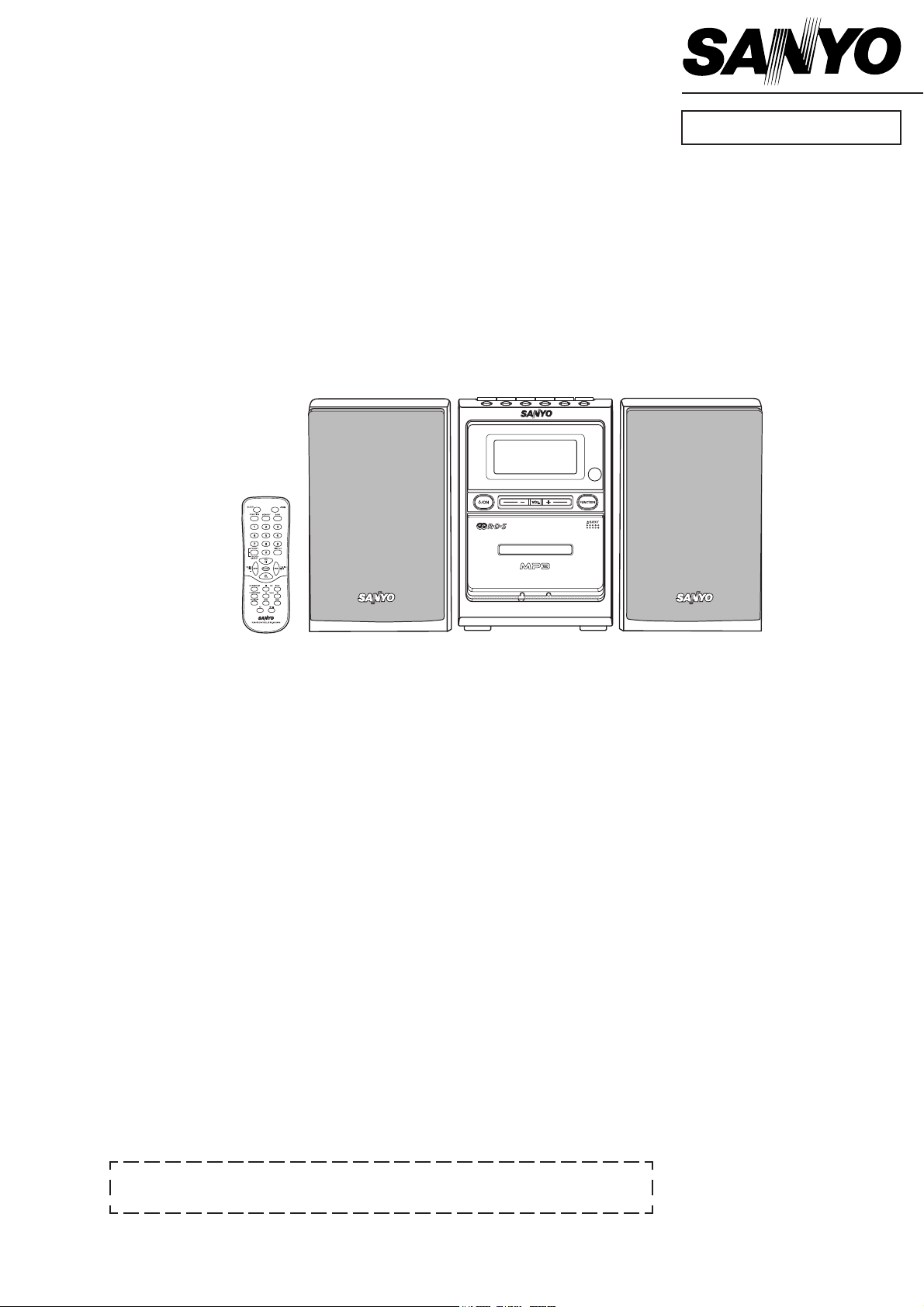
Micro Component System
DC-DA3300M (XE)
Contents
Laser beam safety precaution .......................................... 1
Tape adjustments ............................................................ 1
Tuner adjustments ........................................................... 2
CD pick-up maintenance .................................................. 2
Exploded view .................................................................. 3
Parts list ........................................................................... 4
IC block diagram & description ........................................ 7
LCD display description ................................................... 17
Wiring connection ............................................................ 18
This service manual consists of "DC-DA3300MU/XE" (Main unit : 129 700 02) and
"SX-DA3300M/XE" (Speaker system : 165 114 01).
Schematic diagram
(FRONT) ....................................................................... 20
(CD)............................................................................... 22
(TUNER) ....................................................................... 26
(AMPLIFIER) ................................................................. 30
Wiring diagram
(BUTTON-FRONT) ....................................................... 19
(BUTTON-TOP) ............................................................ 19
(LED) ............................................................................. 19
(FRONT & CD) .............................................................. 24
(TUNER) ....................................................................... 28
(POWER TRANSFORMER) ......................................... 29
(AMPLIFIER) ................................................................. 32
PRODUCT CODE No.
129 701 02
REFERENCE No. SM5810675
Page 2
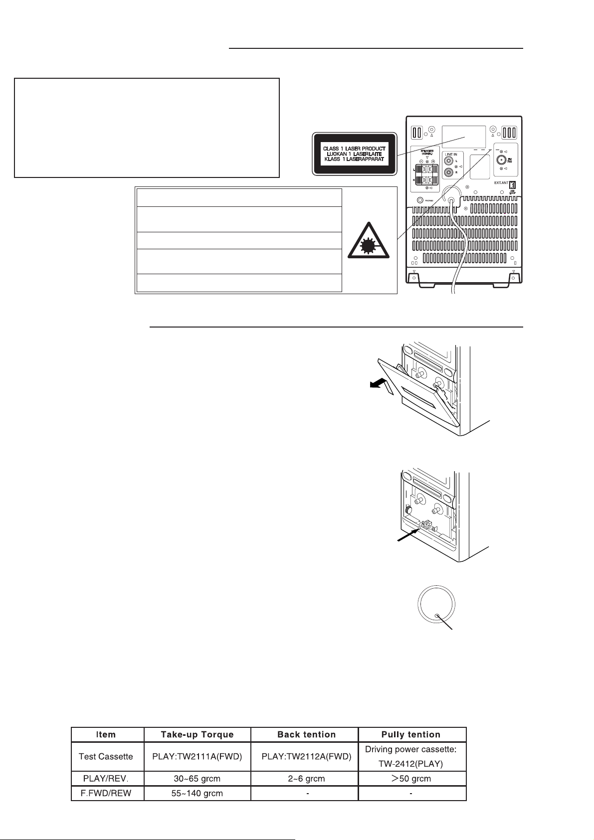
LASER BEAM SAFETY PRECAUTION
• Pick-up that emits a laser beam is used in this CD player section.
CAUTION :
THIS PRODUCT CONTAINS A LOW POWER LASER DEVICE,
TO ENSURE CONTINUED SAFETY DO NOT REMOVE ANY
COVERS OR ATTEMPT TO GAIN ACCESS TO THE INSIDE
OF THE PRODUCT.
REFER ALL SERVICING TO QUALIFIED PERSONNEL.
LASER OUTPUT ..............0.6 mW Max. (CW)
WAVELENGTH ..................790 nm
CAUTION – INVISIBLE LASER RADIATION WHEN OPEN AND
INTERLOCKS DEFEATED. AVOID EXPOSURE TO BEAM.
ADVARSEL – USYNLIG LASER STRÅLING VED ÅBNING, NÅR
SIKKERHEDSAFBRYDERE ER UDE AF FUNKTION, UNDGÅ UDS ÆTTELSE
FOR STRÅLING.
VARNING – OSYNLIG LASER STRÅLNING NÄR DENNA DEL ÄR ÖPPNAD
OCH SPÄRR ÄR URKOPPLAD. STRÅLEN ÄR FARLIG.
VORSICHT – UNSICHTBARE LASERSTRAHLUNG TRITT AUS, WENN
DECKEL GEÖFFNET UND WENN SICHERHEITSVERRIEGELUNG
ÜBERBRÜCKT IST. NICHT, DEM STRAHL AUSSETZEN.
VARO – AVATTAESSA JA SUOJALUKITUS OHITETTAESSA OLET ALTTIINA
NÄKYMÄTTÖMÄLLE LASERSÄTEILYLLE. ÄLÄ KATSO SÄ
TAPE ADJUSTMENTS
1. Azimuth Adjustment
TEESEEN.
• Be sure to clean the heads before attempting to make any adjustment.
• Be sure both channels (1 and 2) are the same level.
(Using a dual-channel oscilloscope)
• Be sure both channel's waveform are same for the phase matching.
• After completion of the adjustment, use the threadlock (TB-1401B) to
secure the azimuth adjustment screws.
1. Remove the cover deck as Fig.1.
2. Load a test tape (VTT-738 etc. : 10kHz) in the Deck.
3. Press the PLAY button. (Normal playback)
4. Use a + tip screwdriver to turn the screw for normal azimuth
adjustment so that the left and right outputs are maximized at
the same phase during normal playback. See Fig.2.
NORMAL
5. Adjust so that the waveforms for the left and right channels are in alignment.
2. Tape Speed Adjustment
• Connect the Frequency Counter to TAPE OUT.
MOTOR
1. Insert the test tape (MTT-111N, etc.; 3,000Hz) into the DECK.
2. Press the PLAY button. .
3. Adjust a hole on the motor bottom so that a frequency counter reading of 3,000 ±5Hz is obtained.See Fig.3.
4. Press the STOP button, and eject the test tape.
Fig.1
Fig.2
hole for adjustment
Fig.3
3. Torque Measurement
- 1 -
Page 3
(MW)
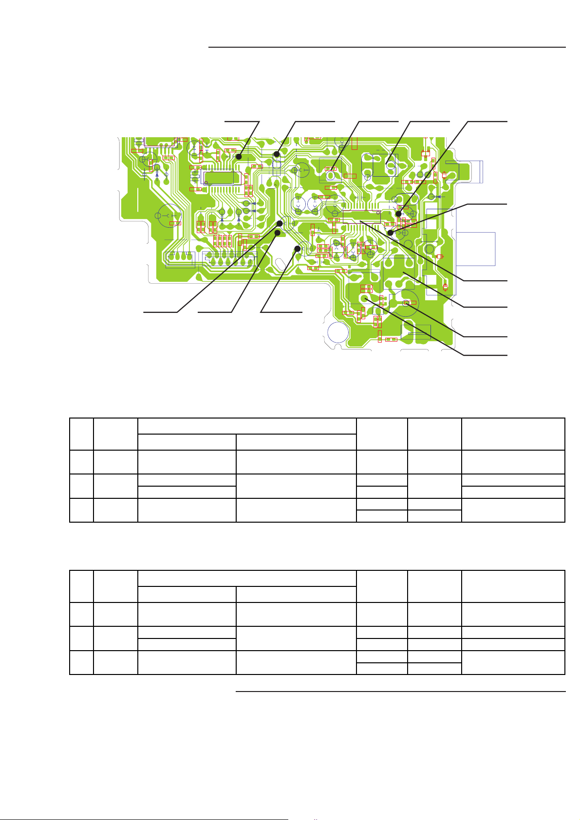
TUNER ADJUSTMENTS
R2201
R2205
C2203
R2458
R2203
R2202
C2304
R2302
C2323
C2310
C2308
R2312
R2309
R2308
R2306
C2902
C2101
C2318
R2107
R2101
C2325
C2141
C2152
C2502
C2504
C2515
C2521
C2456
R2453
• Use a plastic screw driver for adjustments. • MODE : ST (Stereo)
• TUNING
FM : 87.5 - 108MHz
C2512
X2501
C2513
L2502
C2505
C2504
C2504
C2506
IC251
R2521
C2515
C2515
D2451
C2901
J2220
L2501
C2902
C2902
C2503
C2502
C2502
C2521
C2521
RST
R2522
C2457
RDCL
RDDA
C2454
X2451
C2453
J2346
C2461
READY
AM : 522 - 1611kHz (9kHz steps)
520-1610kHz(10kHz steps)
T002A 94V-0
1AV4B10D2741C
C2516
CN206
J2422
C2903
L2451
C2451
C2456
C2456R2453
C2455
R2453
IC241
J2347
C2462
C2464
C2463
R2461
GND
TU_CE
D2452
R2455
J2342
C2117
R2452
C2452
D2453
D2454
R2464
R2463
R2462
CN205
TU_DATA
TU_CLK
TU_R
A_GND
TU_L
TU_DO
E
Q2451
Q2201
J2416
C2322
R2460
J2348
J2349
R2801
R2812
R2712
+5.6V
+9.4V
R2205
R2205
E
R2458
R2458
R2459
D2466
D2456
R2701
XF221
R2201
R2201
R2204
J2215
VT
J2356
C2102
C2203
C2203
R2203
R2202
R2203R2202
J2343
VT
J2216
J2417
C2328
J2350
C2327
TP13TP14TP15
J2418
J2217
C2305
J2421
C2101
C2101
J2212
C2321
J2354
R2108
C2170
R2101
R2101
R2301
R2107
R2107
C2306
C2319
R2310
L
C2115
XF233
R2304
R2305
R2306
R2306
J2345
C2316
R2307
C2309
C2314
J2211
R2114
C2324
R2309
R2309
R2103
C2320
C2307
R2311
J2357
C2116
R2112
R2308
R2308
R2454
R2102
R2111
J2419
C2302
C2301
IC231
C2317
C2310
C2310
C2308
C2318
C2308
C2318
R2312
R2312
J2355
C2154
R2131
L2153
R2149
R2148
J2213
XF231
C2303
C2311
J2351
J2352
C2152
C2152
C2151
R2151
D2153
C2029
T2002
J2420
J2218
C2315
R2901
U2101
J2214
R2331 C2332
XF222
C2325
C2325
C2304
C2304
C2312
R2302
C2323
R2302
C2323
C2313
L2151
C2141
C2141
CT252
S2001
T2002XF233
Q2310
E
Q2140
E
L
R2140
R2141
J2344
D2151
R2100
D2104
C2140
D2152
D2103
TP24TP11TP12
CN202
TP25
CN201
IC231
L2151
CT252
L2153
Antenna : 75Ω unbalanced direct, Modulation : 1 kHz
Dev. : ±22.5kHz(MONO), ±22.5kHz(MAIN), ±6.75kHz(PILOT)
RF Level : dBuV EMF
1. FM
Adjusting
Step
Circuit
IF(0V)
1
Adjustment
Cover
2
Voltage
3 Tracking
Connection
Input Output
FM Antenna SG=66dBuV IC231 3-22pin(TP24,25) 98.0MHz XF233
--- 87.5MHz 1.37±0.5V Check Only
--- 108.0MHz 6.9±0.50V Check Only
FM Ant ---TP13(L), TP14(E) and TP15(R)
Output Level : about 30mV at TP13, TP14, TP15
SG
Frequency
TP11(H), TP12(E)
90.0kHz ---
106.0kHz ---
Adjustment
Alignment parts is XF233.
IC231(3-22pin)0.0±0.05V
---
Anntena : IRE Loop(SG), Moduration : 1kHz 30%
RF Level : dBuV EMF
2. AM
Adjusting
Step
CD PICK-UP MAINTENANCE
Circuit
IF
1
2
3 Loop Ant
Adjustment
Cover
Voltage
Tracking
(MW)
Input Output
Loop Ant TP13(L), TP14(E) and TP15(R)
--- 522kHz L2153 1.00±0.05V
--- 1611kHz --- 7.90±0.50V Check Only
About pick-up (Optical lens) Cleaning
Clean a lens with swab of the cotton which moistened it with alcohol, cleaning paper or cleaning disc appointed.
Connection
Output Level : about 30mV at TP13, TP14, TP15
SG
Frequency
450kHz
at 999kHz
Adjustment
T2002
TP11(H )and TP12(E)
TP13(L), TP14(E) and TP15(R)
603kHz L2151
1404kHz CT252
Specified cleaning disc : LC-1 (Part code : 645 026 1961 ..... manufactured by SANYO.)
Show a clean procedure in the following in reference by swab of cotton.
1. Cotton swab is wrapped with Cleaning paper.
2. Add the isopropyl alcohol.
3. Gently move the tip of cotton swab just like a draw a whirlpool from inside to outside on the surface of lens.
- 2 -
Remark
Remark
Maximum
Maximum
Page 4
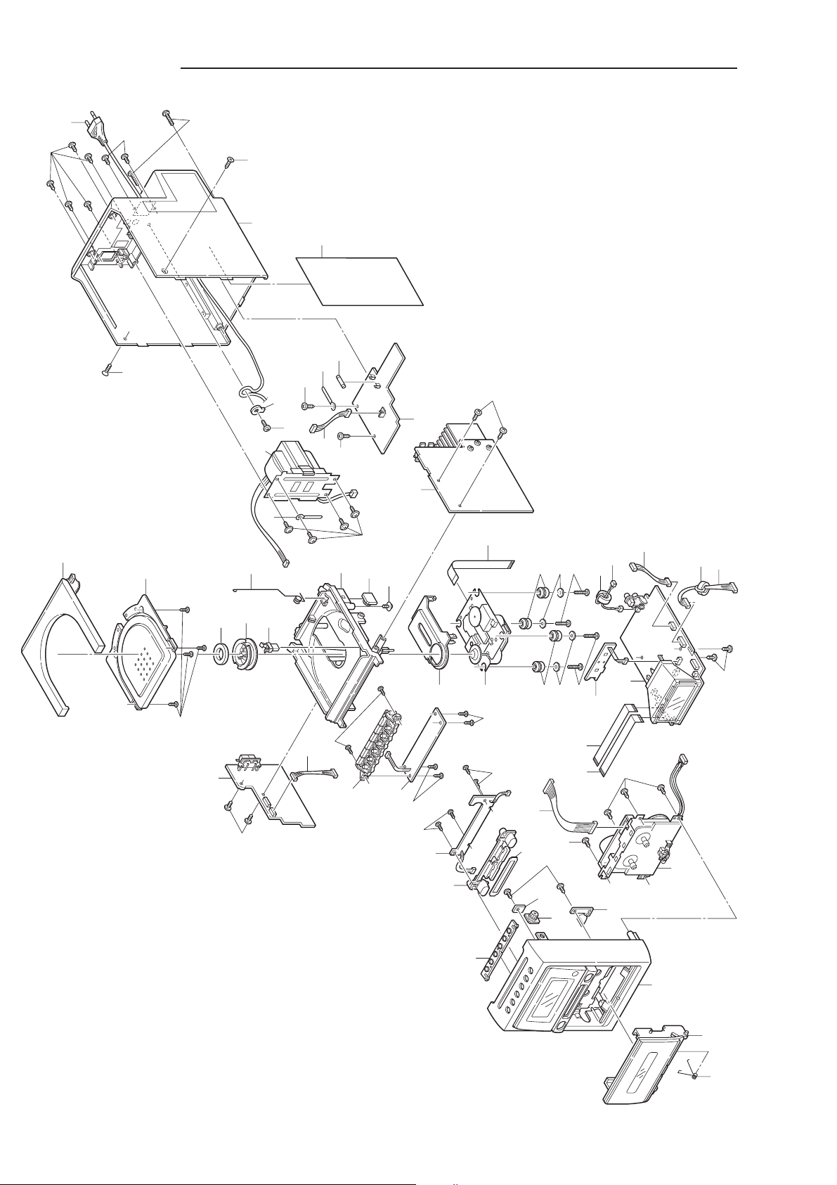
EXPLODED VIEW
1
2
3
5
4
6
7
8
9
71
73
51
52
53
54
55
57
56
58
59
60
63
Y16
11
13
72
12
74
14
16
17
18
19
15
20
21
11
10
75
76
77
22
N.S.P.
62
61
64
23
N.S.P.
Y02
Y01
Y01
Y03
Y04
Y04
Y10
Y13
Y14
Y15
Y15
Y17
Y18
Y18
Y19
Y20
Y20
Y11
Y09
Y12
Y05
Y03
Y06
Y07
Y07
Y08
Y87
This is a basic exploded view.
- 3 -
Page 5

PARTS LIST
PRODUCT SAFETY NOTICE
EACH PRECAUTION IN THIS MANUAL SHOULD BE FOLLOWED DURING SERVICING. COMPONENTS IDENTIFIED WITH THE
!!
IEC SYMBOL
PERFORMANCE CAN BE OF SPECIAL SIGNIFICANCE. WHEN REPLACING A COMPONENT IDENTIFIED BY
REPLACEMENT PARTS DESIGNATED, OR PARTS WITH THE SAME RATINGS OF RESISTANCE, WATTAGE OR VOLTAGE THAT
ARE DESIGNATED IN THE PARTS LIST IN THIS MANUAL. LEAKAGE-CURRENT OR RESISTANCE MEASUREMENTS MUST BE
MADE TO DETERMINE THAT EXPOSED PARTS ARE ACCEPTABLY INSULATED FROM THE SUPPLY CIRCUIT BEFORE
RETURNING THE PRODUCT TO THE CUSTOMER.
CAUTION : Regular type resistors and capacitors are not listed. To know those values, refer to the schematic diagram.
N.S.P : Not available as service parts.
!
IN THE PARTS LIST AND THE SCHEMATIC DIAGRAM DESIGNATED COMPONENTS IN WHICH SAFETY AND
!!
!
, USE ONLY THE
Regular type resistors are less than 1/4 W carbon type and 0 ohm chip resistors.
Regular type capacitors are less than 50 V and less than 1000 µF type of Ceramic type and Electrical type.
PACKING & ACCESSORIES
REF.NO. PART NO. DESCRIPTION
614 332 3228 CARTON CASE
614 330 7464 CUSHION,FRONT
614 330 7471 CUSHION,REAR
614 332 3242 INSTRUCTION MANUAL
614 332 3259 INSTRUCTION SHEET
645 063 7483 ASSY,ANTENNA,LOOP
614 229 4635 FM ANTENNA
or 614 308 5515 FM ANTENNA
645 071 0988 REMOCON,RB-DA3300M
614 332 5888 LID,BATTERY REMOCON
614 332 6106 ASSY,BOX,SPEAKER
CABINET & CHASSIS
REF.NO. PART NO. DESCRIPTION
1 614 330 7419 SPRING,DOOR DECK
2 614 332 6236 ASSY,DOOR,DECK
3 614 332 6243 ASSY,PANEL FRONT
4 614 329 8441 ASSY,MECHA,TM-PT70TN-SH
(For details to page7.)
5 614 330 9932 LATCH,CAM,DECK DOOR,LOCKING
6 614 309 7969 ASSY,GEAR,LID,CASSETTE
7 614 330 7280 DEC,BUTTON
8 614 330 9673 PANEL,VOL
9 614 330 7235 BUTTON,FRONT
10 614 330 7211 BUTTON,TOP,6 KEYS+6 KEYS
11 614 310 3899 SPACER,MECHA,MTG CD+DA11
12 614 325 6014 ASSY,MECHA,DA11T3CN-SASH
or 614 333 0387 ASSY,MECHA,DA11V
13 614 307 2072 COVER,PICK-UP
14 614 322 2125 ASSY,GEAR,LID,CD
15 614 330 7389 MOUNTING,CD
16 614 330 7402 SPRING,DOOR CD
17 614 303 0263 LATCH,PUSH,CD DOOR,LOCKING
18 614 307 8821 PULLEY
19 614 303 0256 LATCH,MAGNET
20 614 330 7297 DEC,WINDOW CD
21 614 330 7372 LID,CD
22 614 332 9060 SHIELD,RIGHT
23 614 332 6229 ASSY,CABINET,REAR
FIXING PARTS
REF.NO. PART NO. DESCRIPTION
Y01 411 021 3503 SCR S-TPG BIN 3X10,
F-PANEL+DECK,MECHA
Y02 411 021 3503 SCR S-TPG BIN 3X10,
F-PANEL+LATCH CAM,
F-PANEL+ASSY GEAR DECK
Y03 411 098 4700 SCR S-TPG BIN 2.3X8,
PWB,FRONT+BUTTON,FRONT
Y04 411 098 4700 SCR S-TPG BIN 2.3X8,
PWB,TOP+BUTTON,TOP
Y05 411 098 4700 SCR S-TPG BIN 2.3X8,
BUTTON,TOP+F-PANEL
Y06 411 021 3503 SCR S-TPG BIN 3X10,
PWB,CD+MTG,CD
REF.NO. PART NO. DESCRIPTION
Y07 411 021 1806 SCR S-TPG BIN 2.6X10,
MTG,CD+CD11
Y08 411 092 0906 WASHER Z 2.6X10X0.5,
MTG,CD+CD11
Y09 411 021 6405 SCR S-TPG BIN 3X8,
PWB,MAIN+MTG,CD
Y10 412 032 6408 SPECIAL SCREW,
MTG.CD+ASSY,GEAR CD
Y11 411 021 3503 SCR S-TPG BIN 3X10,
PWB,TUNER+MTG,CD
Y12 411 187 2709 SCR S-TPG BIN 2.3X6,
LID,CD+WINDOW CD
Y13 411 020 9100 SCR S-TPG BRZ+FLG 3X12,
REAR+P-TRANS
Y14 614 130 0382 LUG
Y15 411 021 3503 SCR S-TPG BIN 3X10,
REAR+PWB,POWER
Y16 614 129 9136 LUG,FOR PT WIRE
Y17 411 021 3503 SCR S-TPG BIN 3X10,AC CORD
Y18 411 098 7800 SCR S-TPG FLT 3X12,
REAR+MTG(L/R)
Y19 411 021 4906 SCR S-TPG BIN 3X20,
REAR+PANEL,FRONT
Y20 411 021 3404 SCR S-TPG BIN 3X10,
REAR+(MTG CD,ANT TERMINAL,
SPEKER TERMINAL,PWB LINE-IN)
ELECTRICAL PARTS
REF.NO. PART NO. DESCRIPTION
51 614 331 8927 ASSY,WIRE,CDF-TAPE MECHA
52 614 331 9009 FLEXIBLE FLAT CABLE,CDF-TU
53 614 331 9016 FLEXIBLE FLAT CABLE,CDF-AMP
54 614 332 6687 ASSY,WIRE,FRONT CD TO TU
55 614 331 8897 ASSY,WIRE,CDF-AMP
56 645 072 6651 CORE,FERRITE
57 614 331 8965 ASSY,WIRE,CDF-CD MECHA
58 614 331 8958 ASSY,WIRE,CDF-AMP AUX-IN
(SHIELDED)
59 645 072 6644 CORE,FERRITE
60 614 332 3372 FLEXIBLE FLAT CABLE,
CD-PICK UP
61 645 072 9928 TRANS,POWER
62 614 332 6694 ASSY,WIRE,DG TO AMP
63 423 016 9704 FUSE 250V 0.5A
64 645 016 9939 CORD,POWER-1.74MK
BUTTON-FRONT P.W.BOARD ASSY
REF.NO. PART NO. DESCRIPTION
71 614 331 8866 ASSY,PWB,
BUTTON-FRONT(Only initial)
CN660 614 332 3303 ASSY,WIRE,CDF-BUTTON FRONT
CN661 614 332 5734 ASSY,WIRE,IR-CDF
DS660 407 235 5006 PHOTO DIODE SPS-444-1-VG
S6610 645 048 3820 SWITCH,PUSH
S6611 645 048 3820 SWITCH,PUSH
S6612 645 048 3820 SWITCH,PUSH
S6613 645 048 3820 SWITCH,PUSH
- 4 -
Page 6

PARTS LIST
REF.NO. PART NO. DESCRIPTION
72 614 331 8859 ASSY,PWB,BUTTON-TOP(Only initial)
CN651 614 331 8910 ASSY,WIRE
S6510 645 048 3820 SWITCH,PUSH
S6511 645 048 3820 SWITCH,PUSH
S6512 645 048 3820 SWITCH,PUSH
S6513 645 048 3820 SWITCH,PUSH
S6514 645 048 3820 SWITCH,PUSH
S6515 645 048 3820 SWITCH,PUSH
S6516 645 048 3820 SWITCH,PUSH
S6517 645 048 3820 SWITCH,PUSH
S6524 645 048 3820 SWITCH,PUSH
S6525 645 048 3820 SWITCH,PUSH
S6526 645 048 3820 SWITCH,PUSH
S6527 645 048 3820 SWITCH,PUSH
FRONT & CD P.W.BOARD ASSY
REF.NO. PART NO. DESCRIPTION
73 614 332 6519 ASSY,PWB,FRONT-CD(Only initial)
AH601 614 330 7358 HOLDER,LCD
AS601 614 330 7334 DEC,SHEET LCD
CN111 645 059 0498 SOCKET,FPC 16P
CN112 645 005 8127 PLUG,6P
CN122 645 005 8141 PLUG,9P
or 614 310 2502 PLUG,9P
CN145 645 012 6369 JACK,RCA-2
CN146 645 005 7373 PLUG,3P
CN601 645 009 4163 SOCKET,FFC 12P
CN602 645 009 4163 SOCKET,FFC 12P
CN604 645 005 8110 PLUG,4P
CN605 645 005 8141 PLUG,9P
CN606 645 005 7366 PLUG,2P
CN610 645 005 7373 PLUG,3P
CN611 645 005 7366 PLUG,2P
CN612 645 005 7373 PLUG,3P
D1501 407 098 3300 DIODE RL153-BF-S2
D1502 407 098 3300 DIODE RL153-BF-S2
D6010 407 012 4406 DIODE 1SS133
D6110 407 012 4406 DIODE 1SS133
D6111 407 012 4406 DIODE 1SS133
D6113 407 012 4406 DIODE 1SS133
D6201 407 099 4603 ZENER DIODE MTZJ3.9B
D6406 407 099 5204 ZENER DIODE MTZJ5.1B
D6960 407 012 4406 DIODE 1SS133
IC101 410 538 0401 IC LC78646E-UHK-E
IC102 410 538 0500 IC LC78684NE-UHK-E
IC103 410 530 7804 IC M12L16161A-7TG
IC104 409 582 6002 IC LA6548NH-E
IC601 410 547 9303 IC LC877464C-54P5-E
JW200 614 332 4034 ASSY,WIRE
L1301 645 002 1459 INDUCTOR,22U K
L1302 645 037 2858 CORE,PIPE
L1303 645 001 4581 INDUCTOR,100U K
L1304 645 001 5519 INDUCTOR,47U K
L1305 645 001 5519 INDUCTOR,47U K
L1306 645 001 5519 INDUCTOR,47U K
L1401 645 037 2858 CORE,PIPE
L1501 645 037 2858 CORE,PIPE
L6010 645 001 5441 INDUCTOR,2.2U K
LCD60 645 071 1107 LCD
PR151 645 066 9668 PROTECTOR,0.4A 125V
Q1301 405 008 7301 TR 2SB810-F
or 405 008 7202 TR 2SB810-E
or 405 008 6809 TR 2SB808-F-SPA
Q1401 405 017 9709 TR 2SC3330-U
or 405 011 8609 TR 2SC1740S-S
or 405 011 8500 TR 2SC1740S-R
or 405 143 8706 TR KTC3199-GR
or 405 017 9600 TR 2SC3330-T
Q1501 405 009 5306 TR 2SB927-T
or 405 009 5207 TR 2SB927-S
or 405 141 3604 TR KTA1273-Y
REF.NO. PART NO. DESCRIPTIONBUTTON-TOP P.W.BOARD ASSY
Q6107 405 014 4509 TR 2SC2412K-R
or 405 011 1006 TR 2SC1623-L6
or 405 146 2206 TR KTC3875-GR
or 405 146 2107 TR KTC3875-Y
Q6108 405 014 4509 TR 2SC2412K-R
or 405 011 1006 TR 2SC1623-L6
or 405 146 2206 TR KTC3875-GR
or 405 146 2107 TR KTC3875-Y
Q6201 405 005 5508 TR 2SA812-M6
or 405 002 0308 TR 2SA1037K-R
or 405 134 5905 TR 2SA1037AK-R
or 405 146 9700 TR KTA1504-GR
Q6410 405 155 0002 TR MPSA56
Q6960 405 155 0002 TR MPSA56
Q6961 405 155 0002 TR MPSA56
Q6962 405 000 3806 TR DTC114YS
or 405 143 0007 TR KRC107M
Q6963 405 000 3806 TR DTC114YS
or 405 143 0007 TR KRC107M
X1451 645 020 9024 OSC,CRYSTAL 16.9344MHZ
X6101 645 032 1627 OSC,CRYSTAL 32.768KHZ
X6102 645 072 1106 OSC,CERAMIC 10.0MHZ
LED P.W.BOARD ASSY
REF.NO. PART NO. DESCRIPTION
74 614 332 6540 ASSY,PWB,LED(Only initial)
CN680 614 331 8934 ASSY,WIRE
D6803 407 244 9705 LED LT5CB1-81-UAC3,VOL BLUE
TUNER P.W.BOARD ASSY
REF.NO. PART NO. DESCRIPTION
75 614 332 0975 ASSY,PWB,TUNER(Only initial)
C2457 403 259 0508 NP-ELECT 1U M 50V
CN201 645 057 1909 TERMINAL,TUNER
CN202 645 004 2683 PLUG,2P
CN205 645 009 4163 SOCKET,FFC 12P
CN206 645 005 8110 PLUG,4P
CT252 645 032 5663 TRIMMER,7PF
D2103 407 149 0807 DIODE 1SS355
D2104 407 149 0807 DIODE 1SS355
D2151 407 012 4406 DIODE 1SS133
D2152 407 149 0807 DIODE 1SS355
D2153 407 105 1602 VARACTOR DI SVC342M-V
or 407 105 1305 VARACTOR DI SVC342L-V
D2451 407 012 4406 DIODE 1SS133
D2452 407 153 7502 ZENER DIODE GZS3.0B
D2453 407 012 4406 DIODE 1SS133
D2454 407 012 4406 DIODE 1SS133
D2456 407 012 4406 DIODE 1SS133
D2466 407 012 4406 DIODE 1SS133
IC231 409 474 3201 IC LA1844ML
IC241 409 439 4502 IC LC72121M-D
IC251 409 433 2702 IC LC72723M
L2151 645 037 2377 TRANS,ANT,796KHZ
L2153 645 065 3568 TRANS,OSC,796KHZ
L2451 645 031 7842 INDUCTOR,100U K
or 645 001 4581 INDUCTOR,100U K
L2501 645 031 7842 INDUCTOR,100U K
or 645 001 4581 INDUCTOR,100U K
L2502 645 031 7842 INDUCTOR,100U K
or 645 001 4581 INDUCTOR,100U K
Q2140 405 014 4509 TR 2SC2412K-R
or 405 011 1006 TR 2SC1623-L6
or 405 146 2107 TR KTC3875-Y
or 405 146 2206 TR KTC3875-GR
Q2201 405 016 0806 TR 2SC2839-E
or 405 151 4103 TR KTC3193-Y
or 405 151 4202 TR KTC3193-O
Q2310 405 011 8500 TR 2SC1740S-R
or 405 143 8706 TR KTC3199-GR
or 405 011 8609 TR 2SC1740S-S
or 405 017 9600 TR 2SC3330-T
- 5 -
Page 7
PARTS LIST
REF.NO. PART NO. DESCRIPTION REF.NO. PART NO. DESCRIPTION
or 405 017 9709 TR 2SC3330-U
Q2451 405 078 2404 TR BN1A4P
or 405 036 3702 TR 2SA1564
or 405 151 5209 TR KRA107M
or 405 000 0904 TR DTA114YS
S2001 645 023 5795 SWITCH,LEVER
T2002 645 046 2023 FILTER,450KHZ
U2101 645 043 6697 TUNER,FM
X2451 645 023 4965 OSC,CRYSTAL 7.2MHZ
X2501 645 035 8326 OSC,CRYSTAL 4.332MHZ
XF221 645 054 1223 CERAMIC FILTER 10.70MHZ
or 645 010 7665 CERAMIC FILTER 10.70MHZ
or 614 240 2917 FILTER,CERAM
XF222 645 054 1223 CERAMIC FILTER 10.70MHZ
or 645 010 7665 CERAMIC FILTER 10.70MHZ
or 614 240 2917 FILTER,CERAM
XF231 645 059 0054 CERAMIC FILTER 450KHZ
or 645 041 9324 CERAMIC FILTER 450KHZ
XF233 645 040 9981 TRANS,IF 10.7MHZ
or 645 039 9923 TRANS,IF 10.7MHZ
AMPLIFIER P.W.BOARD ASSY
REF.NO. PART NO. DESCRIPTION
76 614 332 1149 ASSY,PWB,AMP(Only initial)
C4601 403 057 3503 POLYESTER 0.1U K 50V
C4605 403 061 3605 POLYESTER 0.039U J 50V
C4606 403 061 7702 POLYESTER 4700P J 50V
C4607 403 059 3204 POLYESTER 2200P J 50V
C4608 403 060 2807 POLYESTER 0.027U K 50V
C4743 403 057 3503 POLYESTER 0.1U K 50V
C4843 403 057 3503 POLYESTER 0.1U K 50V
C4950 403 332 7400 ELECT 2200U M 50V
C4984 403 329 3309 ELECT 2200U M 25V
CN428 645 006 1806 PLUG,3P
or 614 319 3456 PLUG,3P
CN440 645 005 8127 PLUG,6P
CN441 645 005 7373 PLUG,3P
CN442 614 310 2441 PLUG,3P
or 645 005 7373 PLUG,3P
CN444 645 005 8141 PLUG,9P
CN446 645 009 4163 SOCKET,FFC 12P
CN455 645 011 6384 JACK,PHONE D3.6,HEADPHONE
or 645 055 1017 JACK,PHONE D3.6,HEADPHONE
CN457 645 024 1147 TERMINAL,SPEAKER
D4280 407 196 5800 DIODE 1N5402BD82
D4281 407 196 5800 DIODE 1N5402BD82
D4282 407 196 5800 DIODE 1N5402BD82
D4283 407 196 5800 DIODE 1N5402BD82
D4284 407 196 5800 DIODE 1N5402BD82
D4991 407 099 6805 ZENER DIODE MTZJ13B
D4992 407 099 6003 ZENER DIODE MTZJ9.1B
D4993 407 148 6701 DIODE 1A3-I
D4994 407 098 3300 DIODE RL153-BF-S2
D4995 407 098 3300 DIODE RL153-BF-S2
D4996 407 012 4406 DIODE 1SS133
D4997 407 148 6701 DIODE 1A3-I
D4998 407 012 4406 DIODE 1SS133
HS401 614 330 7341 HEAT SINK
IC440 409 451 7406 IC AN7348K
IC441 409 614 0701 IC LC75348M-E
IC442 409 451 2104 IC TDA7269
IC443 409 189 3404 IC BA7755A
IC446 409 463 6701 IC KIA7805API
L4600 645 006 1523 INDUCTOR,470U J
L4601 645 006 1523 INDUCTOR,470U J
L4602 645 037 2858 CORE,PIPE
L4603 645 006 1523 INDUCTOR,470U J
L4604 645 037 2858 CORE,PIPE
L4605 645 001 5519 INDUCTOR,47U K
L4606 645 001 5519 INDUCTOR,47U K
L4607 645 001 5519 INDUCTOR,47U K
PR420 645 066 9835 PROTECTOR,4A 125V
PR495 645 066 9705 PROTECTOR,0.8A 125V
PR496 645 066 9767 PROTECTOR,1.25A 125V
Q4320 405 143 8706 TR KTC3199-GR
or 405 017 9600 TR 2SC3330-T
or 405 017 9709 TR 2SC3330-U
or 405 011 8500 TR 2SC1740S-R
or 405 011 8609 TR 2SC1740S-S
Q4321 405 004 5004 TR 2SA608-G-NP
or 405 004 4502 TR 2SA608-F-NP
or 405 141 3505 TR KTA1266-Y
or 405 141 3406 TR KTA1266-GR
Q4501 405 143 0007 TR KRC107M
or 405 000 3806 TR DTC114YS
Q4502 405 143 0007 TR KRC107M
or 405 000 3806 TR DTC114YS
Q4503 405 159 0503 TR KRC107S
or 405 141 5608 TR DTC114YKA
Q4600 405 155 0002 TR MPSA56
Q4601 405 000 3806 TR DTC114YS
or 405 143 0007 TR KRC107M
Q4602 405 141 3307 TR KTC3198-GR
or 405 141 3208 TR KTC3198-Y
or 405 019 2708 TR 2SC536-F-NP
or 405 019 3804 TR 2SC536-G-NP
Q4603 405 141 3307 TR KTC3198-GR
or 405 141 3208 TR KTC3198-Y
or 405 019 3804 TR 2SC536-G-NP
or 405 019 2708 TR 2SC536-F-NP
Q4700 405 075 8607 TR DTC143ZS
or 405 143 9000 TR KRC106M
Q4800 405 075 8607 TR DTC143ZS
or 405 143 9000 TR KRC106M
Q4990 405 138 6403 TR KTD2058Y
or 405 095 1602 TR 2SD2061-E
or 405 095 1701 TR 2SD2061-F
Q4991 405 095 1701 TR 2SD2061-F
or 405 095 1602 TR 2SD2061-E
or 405 138 6403 TR KTD2058Y
Q4992 405 008 2504 TR 2SB698-G
or 405 008 2405 TR 2SB698-F
or 405 141 3703 TR KTA1271-Y
Q4993 405 008 2504 TR 2SB698-G
or 405 008 2405 TR 2SB698-F
or 405 141 3703 TR KTA1271-Y
Q4994 405 143 0007 TR KRC107M
or 405 000 3806 TR DTC114YS
R4743 402 071 1304 FUSIBLE RES 2.2 JA 1/4W
R4843 402 071 1304 FUSIBLE RES 2.2 JA 1/4W
SA401 411 021 3503 SCR S-TPG BIN 3X10
SA402 411 021 3503 SCR S-TPG BIN 3X10
SA403 411 021 3503 SCR S-TPG BIN 3X10
SA404 411 021 5705 SCR S-TPG BIN 3X6
SA405 411 021 5705 SCR S-TPG BIN 3X6
SA406 411 021 5705 SCR S-TPG BIN 3X6
SH101 614 331 1294 SHIELD,MAIN PWB
SH102 614 331 1300 SHIELD,TERMINAL
POWER TRANSFORMER P.W.BOARD ASSY
REF.NO. PART NO. DESCRIPTION
77 614 332 0982 ASSY,PWB,POWER,TRANS
(Only initial)
C4108 403 349 3303 CERAMIC 0.01U M 250V
or 403 366 7803 CERAMIC 0.01U M 250V
CN401 645 006 4760 HOLDER,FUSE
or 645 031 7903 HOLDER,FUSE
CN402 645 006 4760 HOLDER,FUSE
or 645 031 7903 HOLDER,FUSE
CN403 614 017 8203 TERMINAL BOARD
CN404 614 017 8203 TERMINAL BOARD
CN410 645 005 9315 PLUG,2P
CN413 614 310 2441 PLUG,3P
or 645 005 7373 PLUG,3P
D4101 407 097 8009 DIODE MPG06G
D4102 407 097 8009 DIODE MPG06G
- 6 -
Page 8
PARTS LIST
REF.NO. PART NO. DESCRIPTION
D4103 407 097 8009 DIODE MPG06G
D4104 407 097 8009 DIODE MPG06G
D4105 407 099 5402 ZENER DIODE MTZJ6.2B
D4106 407 012 4406 DIODE 1SS133
L4591 645 038 7364 INDUCTOR,70U
PT401 645 067 6178 TRANS,POWER
Q4100 405 141 3307 TR KTC3198-GR
or 405 141 3208 TR KTC3198-Y
or 405 019 3804 TR 2SC536-G-NP
or 405 019 2708 TR 2SC536-F-NP
Q4101 405 023 5306 TR 2SD400-F-MP
or 405 023 5009 TR 2SD400-E-MP
or 405 141 1402 TR KTD863-GR
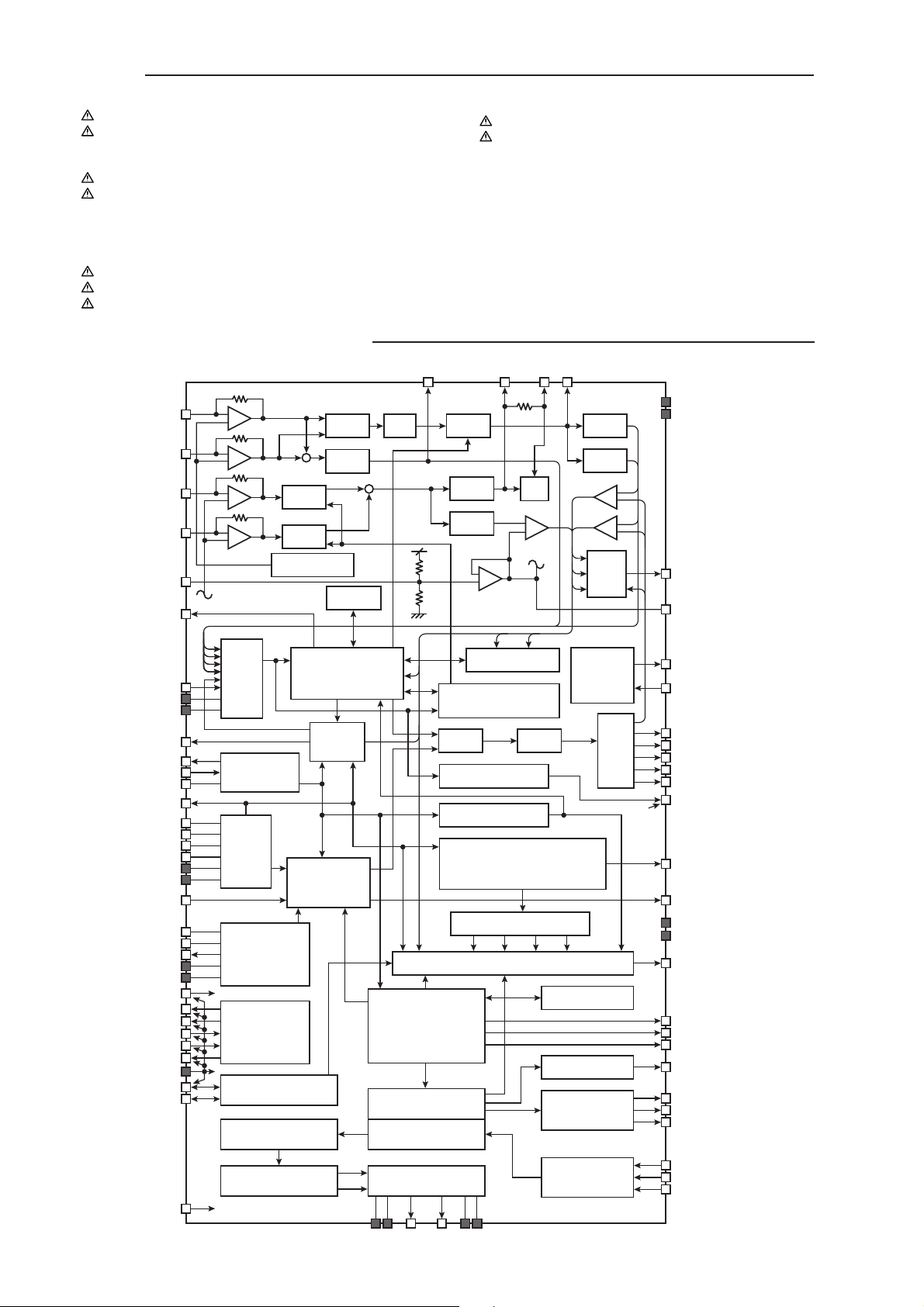
IC BLOCK DIAGRAM & DESCRIPTION
IC101 LC78646E-UHK-E (CMOS LSI for CD Player)
REF.NO. PART NO. DESCRIPTION
RY401 645 035 6575 RELAY
or 645 030 5597 RELAY
TAPE MECHANISM
REF.NO. PART NO. DESCRIPTION
4 614 329 8441 ASSY,MECHA,TM-PT70TN-SH
645 010 9447 PINCH ROLLER(F) ASSY
645 045 1959 RF BELT
645 052 4158 MAIN BELT
645 052 2888 RP HEAD C-9142-BD-1025
645 045 2048 DETECT SWITCH MXS01190
645 067 2934 ASSY,MOTOR
FE
TE
TEC
RF
FIN1
FIN2
TIN1
TIN2
REFI
DEFECT
ADIN
ADAVDD
ADAVSS
JITTC
SLCO
EFMIN
SLCIST
PCK
PDO1
PDO2
FR
PCKIST
VVDD
VVSS
SBCK/FG
XIN
XOUT
16MOUT
XVDD
XVSS
*RES
*WRQ
CL
CE
DI
DO
VDD5V
CONT1,2,3
CONT4,5,
SBCK/CONT6
TEST
+
+
+
+
-
TBAL
TBAL
MIX
+
+
LPF
LEVEL SET
SERVO
A/D
PROCESSEROR
JITTER
DETECT
SLICE LEVEL
CONTROL
PLL
VCEC
CLV,CAV
CONTROL
CLOCK
GENERATOR
COMMAND
INTERFACE
GENERAL-PURPOSE
PORTS
8FS
DIGITAL FILTER
1bit DAC
+
+
-
RAM
INTERPOLATION
EQ
AGC
LPF
LPF
-
+
TRACK JUMP
AUTO ADJUST
SW
DRF
RUPTURE DEFECT
DETECT,PROTECT INSERT
SUBCODE DECODE CRC
MONITOR SIGNAL SELECTOR
ERROR
CORRECTION
AUDIO CD
C1-2,C2-2
MUTE
AT TENUATION
DEEMPHASIS
LPF
SW
+
-
D/A
FRAME SYNC
EFM DECODE
AUDIO OUT
EXTERNAL
PH
BH
MONI
CONT
APC
S/H
RAM
SERIAL
OUT
AUDIO IN
+
-
+
-
VDD5V
RFVDD
RFVSS
RFMON
VREF
LDD
LDS
FDO
TDO
SLDO
SPDO
GPDAC
DRF
FSEQ
V / *P
VDD
VSS
MONI 1~5
FSX/16MIN
C2F
EFLG
DOUT
LRSY
DATACK
DATA
ASLRCK
ASDACK
ASDFIN
LVSS
LVDD
LCHO
- 7 -
RVDD
RCHO
RVSS
Page 9

IC BLOCK DIAGRAM & DESCRIPTION
IC101 LC78646E-UHK-E (CMOS LSI for CD Player)
VVDD
GPDAC
PCKIST
VVSS
CONT4
CONT5
PDO2
SBCK/CONT6
FR
LDD
LDS
1 60
SLCO
2
SLCIST
3
EFMIN
4
RF
5
RFVDD
6
RFVSS
7
FIN1
8
FIN2
9
TIN1
10
TIN2
11
VREF
12
REFI
13
FE
14
TEC
15
TE
16
RFMON
17
JITTC
18
ADAVDD
19
ADAVSS
20
TDO
21 80
22792378247725762675277428732972307131703269336834673566366537643863396240 61
FDO
SLDO
SPDO
Pin
Pin Name
No.
1SLCO O 2SLCIST AI - SLCO output current adjustment resistor connection pin.
3EFMIN I - RF signal input pin.
4RF AO - RF monitor pin.
5RFVDD - - RF power supply pin.
6RFVSS - - RF ground pin. Must be connected to 0V.
7 FIN1 AI - A+C signal input pin.
8 FIN2 AI - B+D signal input pin.
9TIN1 AI - E signal input pin.
10 TIN2 AI F signal input pin.
11 VREF AO RFVDD/2 VREF voltage output pin.
12 REFI AI - Reference voltage seting pin.
13 FE AO ZHI FE signal monitor pin.
14 TEC AO - TE signal LPF capacitor connection pin.
15 TE AO ZHI TE signal monitor pin.
16 RFMON AO ZHI RF internal signal monitor pin.
17 JITTC A - Jitter detection capasitor connection pin.
18 ADAVDD - - Servo A/D, D/A supply pin.
19 ADAVSS - - Servo A/D, D/A ground pin. Must be connected to 0V.
20 TDO AO ADAVDD/2 Tracking control output pin. D/A output.
21 FDO AO ADAVDD/2 Focus control output pin. D/A output.
22 SPDO AO ADAVDD/2 Spindle control output pin. D/A output.
23 SPDO AO ADAVDD/2 Thread control output pin. D/A output.
24 GPDAC AO ADAVDD/2 Servo D/A general-purpose output pin.
25 CONT4 I/O Input mode
26 CONT5 I/O Input mode
27 SBCK/CONT6 I/O Input mode
28 SBCK/FG I -
29 DEFECT O L Defect pin.
30 V / *P O H
31 FSEQ O L
32 MONI 1 O L Internalsignal monitor pin 1.
33 MONI 2 O L Internalsignal monitor pin 2.
34 MONI 3 O L Internalsignal monitor pin 3.
35 MONI 4 O L Internalsignal monitor pin 4.
36 MONI 5 O L Internalsignal monitor pin 5.
37 (3.3V)VSS - -
Reset
I/O
state
Control output.
Slice level
control
General-purpose
input / output pin 4.
General-purpose
input / output pin 5.
General-purpose
input / output pin 6,
or subcode read clock input pin.
Subcode read clock input pin / FG signal input pin /
external emphasis setting pin.
Set to command pin function. Must be connected to 0V.
Rough servo / phase control automatic switching monitor
output pin.
"H" for rough servo and "L" for phase servo.
Synchronization signal detection output pin.
Outputs a high level when the synchronization signal
detected
from the EFM signal and the internally generated
synchronization
signal agree.
Digital ground pin. Must be connected to 0V.
Function description
Controlled by commands
from the microprocessor.
Any of these that are unused
must be either set up as input
pin ports and connected to 0V,
or set up as output pin ports
and left open.
CONT1
CONT2
CONT3
VSS
VDD5V
*RES
*WRQ
DO
CLCEDI
PDO1
DRF
DATA
59
DATACK
58
LRSY
57
ASDFIN
56
ASDACK
55
ASLRCK
54
16MOUT
53
EFLG
52
C2F
51
XVSS
50
FSX/16MIN
49
XIN
48
XOUT
47
XVDD
46
RVDD
45
RCHO
44
RVSS
43
LVSS
42
LCHO
41
LVDD
VDD
V / *P
FSEQ
MONI 1
MONI 2
MONI 3
MONI 4
DEFECT
SBCK/FG
Pin
Pin Name
No.
38 VDD - - Digital power supply pin.
39 DOUT O L Digital OUT output pin.
40 TEST I L Test input pin. Must be connected to 0V.
41 LVDD - 42 LCHO AO LVDD/2 L channel output pin.
43 LVSS - - L channel ground pin. Must be connected to 0V.
44 RVSS - 45 RCHO AO LVDD/2 R channel output pin.
46 RVDD - - R channel power supply pin.
47 XVDD - 48 XOUT O Oscillator Connections for a 33.8688MHz or 16.9344MHz
49 XIN I Oscillator crystal oscillator pin.
50 FSX/16MIN I/O Input mode
51 XVSS - - Crystal oscillator Crystal oscillator ground pin. Must be connected to 0V.
52 C2F O H C2 flag output pin.
53 EFLG O L C1, C2 error correction monitor pin.
54 16MOUT O CLK output 16.9344MHz output pin.
55 ASLRCK I
56 ASDACK I Bit clock input pin. (Must be connected to 0V when unused)
57 ASDFIN I
58 LRSY O L
59 DATACK O L Bit clock output pin.
60 DATA O L L/R channel data output pin.
61 CE I 62 CL I - Data transfer clock input pin.
63 DI I - Data input pin.
64 DO O (H) Data output pin. (Nch open drain output)
65 *WRQ O H Interruption signal output pin.
66 *RES I 67 DRF O L Focus ON detect pin.
68 VDD5V - - Microprocessor interface power supply pin.
69 VSS - - Digital ground pin. Must be connected to 0V.
70 CONT3 I/O Input mode General-purpose output pin 3. Controlled by commands from the microprocessor.
71 CONT2 I/O Input mode General-purpose output pin 2. Must be set as an input pin and connected to 0V
72 CONT1 I/O Input mode General-purpose output pin 1. or set as an output pin and left open when unused.
73 PDO1 O
74 PDO2 O Input mode Phase comparison output pin 2 to control built-in VCO.
75 VVSS - - Built-in VCO GND pin. Must always be connected to 0V.
76 PCKIST AI - Resistor connection pin to set current for PD01 and 02 outputs.
77 VVDD - - Built-in VCO power supply pin.
78 FR AI - Resistor connection pin to set the frequency range of built-in VCO.
79 LDS AI - Laser power detection signal input pin.
80 LDD AO - Laser power detection signal output pin.
Note) The same potential must be supplied to all power supply pins, i. e. , RFVDD, VVDD, ADAVDD, VDD, LVDD,
RVDD AND XVDD. Pins operated from the microprocessor interface power supply (VDD5V) pin :
CE(61 pin), CL(62pin), DI(63 pin), DO(64 pin), *WRQ(65 pin), RES(66 pin), DRF(67 pin), CONT1(72 pin),
CONT2(71 pin), CONT3(70 pin)
MONI 5
Reset
I/O Function description
state
TEST
DOUT
(3.3V)VSS
L channel D/A converter
R channel D/A converter
Crystal oscillator
7.35kHz synchronization signal output pin.
DF, DAC external clock input pin.
Antishock mode
Digital data output
Micro
-processor
interface
Reset input pin.
This pin must be set low briefly after power is first applied.
Phase comparison output pin 1 to control built-in VCO.
PLL
L channel power supply pin.
R channel ground pin. Must be connected to 0V.
Crystal oscillator power supply pin.
L/R clock input pin. (Must be connected to 0V when unused)
L/R channel data input pin.
(Must be connected to 0V when unused)
L/R clock output pin.
Chip enable signal input pin.
IC442 TDA7269 (Stereo Amplifier)
VSS
3
MUTE
5
1
IN-R
+
+
-
-
6
IN-R
- 8 -
IN-L
GND
IN-R
7
9
11
8
10
4
2
OUT-L
IN-L
IN-R
OUT-R
Page 10

IC BLOCK DIAGRAM & DESCRIPTION
IC102 LC78684NE-UHK-E (MP3 Decoder for CD Player)
WEB
CASLB
OEB
MADRS[12:0]
CASUB
RASB
MDATA[15:0]
CL
CMDIN
CE
CMDOUT
INTB
System
CKIN
VPRFR
VCOC
VPDO
CKOUT
WOK
CNTOK
OVF
LRSY
DATACK
DATAIN
C2FIN
SFSY
PW
SBSY
SBCK
Clock-gen
VCO
+
PLL
Anti-Shock
(compression·
incompressible)
RESB
Pin
Pin Name I/ O Block Description
No.
1 LRSY I CD L/R clock input.
2 ADDATA O Audio data output.
3 ADBCK O Audio bit clock output.
4 ADLRCK O Audio L/R clock output.
5 CF2IN I CD IF CD C2 error flag input.
6TEST1 I TEST Test input 1(Must be connected to GND)
7 CKIN I CLOCK System clock(16.9344MHz) input.
8 VSS 9CKOUTOCLOCK Clock(384Fs) output for external DF/DAC
10 TEST2 I TEST Test input 2(Must be connected to GND)
11 DVDD1 12 PW I CD subcode data serial input.
13 SBSY I CD subcode block synchronized signal input.
14 SFSY I CD subcode flame synchronized signal input.
15 SBCK O Serial clock output for CD subcode transfer.
16 AVDD 17 VPRFR - Pin to set the oscillation range of VCO.
18 VCOC I VCO control voltage input.
19 VPDO O VCO charge pump output.
20 AVSS - Analog GND earth terminal.
21 DVDD2 - Power supply pin for internal logic.
22 VSS - GND earth terminal.
23 MDATA0 I/O DRAM data bass 0
24 MDATA1 I/O DRAM data bass 1
25 MDATA2 I/O DRAM data bass 2
26 MDATA3 I/O DRAM data bass 3
27 MDATA4 I/O DRAM data bass 4
28 MDATA5 I/O DRAM data bass 5
29 MDATA6 I/O DRAM data bass 6
30 MDATA7 I/O DRAM data bass 7
31 DVDD3 - Digital power supply pin for I/O.
32 VSS - GND earth terminal.
33 MDATA8 I/O DRAM data bass 8
34 MDATA9 I/O DRAM data bass 9
35 MDATA10 I/O DRAM data bass 10
36 MDATA11 I/O DRAM data bass 11
37 MDATA12 I/O DRAM data bass 12
38 MDATA13 I/O DRAM data bass 13
39 MDATA14 I/O DRAM data bass 14
40 MDATA15 I/O DRAM data bass 15
41 RASB O RAS output(L-active) for EDO-DRAM, SDRAM.
42 WEB O WE output(L-active) for EDO-DRAM, SDRAM.
43 CASLB O
44
CASUB O
OEB O
45
46 MADRS12 O DRAM address output 12
47 MADRS11 O DRAM address output 11
48 MADRS10 O DRAM address output 10
49 MADRS9 O DRAM address output 9
50 MADRS8 O DRAM address output 8
Audio IF
Power
supply
Power
supply
Subcode
IF
Power
supply
PLL
Power
supply
Memory
IF
Power
supply
Memory
IF
GND earth terminal.
Digital power supply pin for I/O.
Analog(PLL) Power supply.
CAS output(For lower byte, L-active)
when use EDO-DRAM.
Clock output for DRAM when use SDRAM.
CAS output(For upper byte, L-active)
when use EDO-DRAM.
CAS output for SDRAM.(L-active)
OE output(L-active) when use EDO-DRAM.
CS output (L-active) when use SDRAM.
DRAM-I /F
CDROM
Decoder
CPU- I / F
Data- I / F
STREQ
STCK
STDAT
CRCF
MP3
Decoder
FSYNC
M
U
X
ADLRCK
Audio- I / F
Pin
Pin Name I / O Block Description
No.
51 DVDD4 - Digital power supply pin for I/O.
52 VSS - GND earth terminal.
53 MADRS7 O DRAM address output 7
54 MADRS6 O DRAM address output 6
55 MADRS5 O DRAM address output 5
56 MADRS4 O DRAM address output 4
57 MADRS3 O DRAM address output 3
58 MADRS2 O DRAM address output 2
59 MADRS1 O DRAM address output 1
60 MADRS0 O DRAM address output 0
61 DVDD5 - Power supply pin for internal logic.
62 VSS - GND earth terminal.
63 STREQ I/O
STCK I/O64
65
STDAT I/O
66 FSYNC O MP3-dec
67
CRCF
68 DVDD6 - Digital power supply pin for I/O.
69 VSS - GND earth terminal.
70 WOK I
71 CNTOK O
72 OVF O
73 CMDOUT O Command serial data output. (Nch open drain output pin)
74 CMDIN I Command serial data input.
75 CL I Command serial clock input.
76 CE I Command enable input.(H-active)
77 INTB O
78 RESB I System reset (L-active)
79 DATAIN I CD serial data input.
80 DATACK I CD bit clock input.
O
Power
supply
Memory
IF
Power
supply
MP3
Stream
Input /
output
CD
monitor
Power
supply
Anti
shock
/MP3
input
&
output
Micon
I/F
CD I/F
When EDO-DRAM use. MP3 data request flag
output.(H-active)
/ DRAM data request flag input(CD ROM : H-active)
When SDRAM use CKE output(L-active).
When EDO-DRAM use. MP3 data transfer clock input.
/ DRAM data transfer clock output.
When SDRAM use DQML output(L-active).
When EDO-DRAM use. MP3 data serial input
/ DRAM data serial output.
When SDRAM use DQMH output(L-active).
MP3 flame synchronized signal(H-active)
/ Complete detection flag of data connecting
point request(CD-DA : H-active)
When EDO-DRAM use. CRC check (CDROM data / CDDA
subcode data) Result output(H-active)
/ DRAM data output enable flag(H-active)
When SDRAM use ADRS13 output.
DRAM light permission input(CD-DA : H-active)
DRAM data request flag input(Only when EDO-DRAM used.)
Complete detection flag of data connecting point request
(CD-DA : H-active) SYNC error monitor flag (MP3 : H-active)
DRAM data serial output(Only when EDO-DRAM used.)
DRAM light interrupt flag(CD-DA : H-active)
Emphasis output flag (MP3 : H-active)
DRAM data transfer clock output.
(Only when EDO-DRAM used.)
Interrupt signal output (L-active)
DRAM light interrupt flag(CD-DA : H-active)
ADBCK
ADDATA
- 9 -
Page 11

IC BLOCK DIAGRAM & DESCRIPTION
IC103 M12L16161A-7TG (Synchronous DRAM)
I/O Control Output Buffer
CLK
ADD
Address Register
LCKE
LRAS
CLK
CLK
CS
CKE
A0~A10/AP
BA
RAS
CAS
WE
L(U)DQM
Bank select
Refresh Counter
Row Buffer
LRAS
LCBR
Timing Register
CKE
PIN NAME
CS RAS CAS WE L(U)DQM
System Clock
Chip Enable
Clock Enable
Address
Bank Select Address
Row Address Strobe
Column Address Strobe
Write Enable
Data Input / Output Mask
Data Input Register
Row Decoder
Col. Buffer
Latency & Burst Length
Programming Register
LCASLWELCBR
Active on the positive going edge to sample all inputs.
Disables or enables device operation by masking or enabling all inputs except CLK,CKE
and L(U)DQM.
Makes system clock to freeze operation from the next clock cycle.
CKE should be enabled at least one cycle prior to new command.
Disable input buffers for power down in standby.
Row / column addresses are multiplexed on the same pins.
Row address : RA0~RA10, column address : CA0~CA7
Selects bank to be activated during row address latch time.
Selects bank for read/write during column address latch time.
Latches row addresses on the positive going edge of the CLK with RAS low.
Enables row access & precharge.
Latches column addresses on the positive going edge of the CLK with CAS low.
Enables column access.
Enables write operation and row precharge.
Latches data in starting from CAS, WE active.
Makes data output Hi-Z tSHZ after the clock and masks the output.
Blocks data input when L(U)DQM active.
512K X 16
X
512K
16
Column Decoder
LWCBR
Input Function
Sense AMP
LDQM
LWE
LDQM
DQi
VDD
DQ0
DQ1
V
SSQ
DQ2
DQ3
DDQ
V
DQ4
DQ5
V
SSQ
DQ6
DQ7
DDQ
V
LDQM
WE
CAS
RAS
CS
BA
A10/AP
A0
A1
A2
A3
V
DD
1
2
3
4
5
6
7
8
9
10
11
12
13
14
15
16
17
18
19
20
21
22
23
24
25
50
49
48
47
46
45
44
43
42
41
40
39
38
37
36
35
34
33
32
31
30
29
28
27
26
VSS
DQ15
DQ14
V
SSQ
DQ13
DQ12
DDQ
V
DQ11
DQ10
V
SSQ
DQ9
DQ5
DDQ
V
N.C/RFU
UDQM
CLK
CKL
N.C
A9
A8
A7
A6
A5
A4
V
SS
IC104 LA6548NH-E (CD Driver)
PIN No. Pin Name Description (Function) PIN No. Pin Name Description (Function)
1
2
3
4
5
6
7
8
9
10
11
12
13
14
15
VCC1
MUTE
VIN1
VG1
VO1+
VO1(NC)
(NC)
VO2VO2+
VG2
VIN2
REG_C
REG_B
RESET
Power supply (VCC2, short-circuit 28pin)
Output ON/OFF terminal
CH1, Input terminal
CH1, Input terminal(Gain setting)
CH1, Output terminal(+)
CH1, Output terminal(-)
(Do not use)
(Do not use)
CH2, Output terminal(-)
CH2, Output terminal(+)
CH2, Input terminal(Gain setting)
CH2, Input terminal
External PNP Connect to transistor collector
External PNP Connect to transistor base
RESET output
- 10 -
16
17
18
19
20
21
22
23
24
25
26
27
28
CD
VIN3
VG3
VO3+
VO3(NC)
(NC)
VO4VO4+
VG4
VIN4
VREF
VCC2
RESET Connect to condenser
of dalay time setting
CH3, Input terminal(Gain setting)
CH3, Input terminal(Gain setting)
CH3, Output terminal(+)
CH3, Output terminal(-)
(Do not use)
(Do not use)
CH4, Output terminal(-)
CH4, Output terminal(+)
CH4, Input terminal(Gain setting)
CH4, Input terminal(Gain setting)
Standard applied voltage terminal
Power supply
(VCC1, short-circuit 1pin)
Page 12

IC BLOCK DIAGRAM & DESCRIPTION
IC104 LA6548NH-E (CD Driver)
REG_B
REG_C
VIN2
VG2
VO2+
VO2-
(NC)
(NC)
VO1-
VO1+
VG1
VIN1
MUTE
VCC1
14
External PNP transistor, Base connect
13
External PNP transistor, Collector connect
12
+
11
11k 11k
-
15.4k 15.4k
Level shift
3.3VREG
Level shift
RESET
+
-
15
RESET
16
CD
17
VIN3
19
VG3
10
19
VO3+
9
20
VO3-
8
21
(NC)
FR
+
FR
-
GNDGND
7
22
(NC)
6
5
Level shift
Level shift
VO4-
24
VO4+
23
4
25
VG4
+
+
3
2
11k
(Output ON/OFF)
MUTE
15.4k
15.4k
-
11k
+
VIN4
27
VREF
26
1
-
28
VCC2
IC231 LA1844ML (Home Audio Tuner IC)
24 23 22 21 20 19 18 17 16 15 14
ALC
BUFF
LEVEL
DET
FM
IF
1
AM
OSC
S-CURVE
FM
DET
23456789101112
AM
MIX
REG
AM/FM
IF
BUFF
AM
RF.AMP
AGC
AM
IF
COMP
TUNING
GND
DET
DRIVE
AM
P-DET
VCO
304kHz
DECODER
ANTI-BIRDIE
STEREO
SW
FF
38k
VCC
FF
19k
2
PILOT
CANCEL
FF
19k
13
PILOT
DET
- 11 -
Page 13

IC BLOCK DIAGRAM & DESCRIPTION
IC241 LC72121M-D (Pll Synthesizer)
2
Vssx
XIN
XOUT
FMIN
17
1
24
1/2
REFERENCE
DIVIDER
SWALLOW COUNTER
1/16, 1/17 4bits
PHASE DETECTOR
CHARGE PUMP
UNLOCK
DETECTOR
19
20
22
21
PD
AIN
AOUT
Vssa
16
AMIN
CE
3
DI
CL
DO
V
Vssd
4
5
6
DD
18
15
CCB
I / F
POWER
ON
RESET
IC440 AN7348K (Play/REC Pre Amplifier)
L-PB AMP
R-PB AMP
L-PB NF
L-PB EO
21222324
12bits PROGRAMMABLE
DIVIDER
DATA SHIFT REGISTER LATCH
9
8
7
BO1BO2 BO3 BO4
L-PB
10 11
AMP OUT
ALC
20
14
IO2
IO1
L-REC IN
1819
UNIVERSAL
COUNTER
L-REC OUT
17
16
ALC
P
15
R
13
HI/LO
IFIN
CRO/NOR
VCC
1314
A/Rec
B
A/Rec
1
L-PB AMP
B
2
R-PB AMP
PB Amp(L)
PB Amp(R)
3
R-PB NF
Mute
Mute
4
R-PB EO
ALC
Logic
A/B
5
R-PB OUT
- 12 -
6
AB SW
Amp(R)
7
R-REC IN
Rec
Amp(L)
Rec
Logic
Rec/PB
8
9
R-REC OUT
P
R
Nor/Cro
& Hi/Lo
Logic
R
P
10 1211
A/B SW
REC/PB SW
Ripple
Rejection
GND
FILTER
Page 14

IC BLOCK DIAGRAM & DESCRIPTION
/
IC251 LC72723M (RDS Demodulation LSI)
VREF FLOUT CIN
Vdda
Vssa
MPXIN
TEST
REFERENCE
VOLTAGE
57kHz
ANTIALIASING
FILTER
TEST
RDS-ID/ READY
RDCL
RDDA
RST
MODE
(SCF)
Vddd
BPF
Vssd
1611521431341251161079
VREF
MPXIN
Vdda
Vssa
CIN
FLOUT
TEST
XIN
8
XOUT
+
-
PLL
(57kHz)
CLOCK
RECOVERY
(1187.5Hz)
VREF
SMOOTHING
FILTER
CLK(4.332MHz)
OSC
DATA
DECODER
RAM
(128bit)
RDS-ID
DETECT
XIN XOUT
PIN NO. PIN NAME I/O Description
1 VREF O Reference Voltage Output (Vdda/2)
2 MPXIN I Base Band (Maltiplex) Signal Input
5 FLOUT O Sub Careea Output (Filter Output)
6 CIN I Sub Careea Input (Comparator Input)
3 Vdda - Analog System Power Supply (+5V)
4 Vssa - Analog System Ground
8 XOUT O Crystal Oscillator Output (4.332MHz)
9 XIN Crystal Oscillator Input (External Reference Signal Input)
7 TEST Test Input
12 MODE Reading Mode Setting (0: Master, 1: Slave)
13 RST RDS-ID/RAM Reset (Straight Polarity)
14 RDDA O RDS Data Output
15 RDCL I/O
RDS-ID/
16
READY
11 Vddd - Digital System Power Supply (+5V)
10 Vssd - Digital System Ground
I
RDS Clock Output (Master Mode) /
RDS Clock Input (Slave Mode)
O RDS-ID/READY Output (Negative Polarity)
Vddd
Vssd
RDDA
RDCL
MODE
RST
RDS-ID
READY
1 4 52 3
IC446 KIA7805API (Regulator)IC443 BA7755A (Rec/Play Switch)
1. INPUT
2. COMMON
3. OUTPUT
123
- 13 -
Page 15

IC BLOCK DIAGRAM & DESCRIPTION
IC441 LC75348M-E (Electronic Volume)
LSELO LIN LTRE LBASS1 LBASS2 LOUT
10 9 8
L4
11
L3
12
L2
13
L1
NC
NC
R1
R2
R3
R4
14
15
16
17
18
19
20
-
+
MULTIPLEXER
CONTROL
CIRCUIT
+
-
MULTIPLEXER
-
+
ZERO CROSSDET
ZERO CROSSDET
ZERO CROSSDET
+
-
76 5
-
-
+
+
-
+
LVref
CCB
INTERFACE
RVref
NO SIGNAL
TIMER
+
-
+
-
+
4
3
2
1
30
29
28
27
TEST
VSS
CE
DI
CL
VDD
Vref
TIM
21 22 23
24 25 26
RSELO RIN RTRE RBASS1 RBASS2 ROUT
Pin Name Pin No. DESCRIPTION Pin Name Pin No. DESCRIPTION
L1
L2
L3
L4
R1
R2
R3
R4
LSELO
RSELO
LBASS1
LBASS2
RBASS1
RBASS2
LIN
RIN
LOUT
ROUT
LT RE
RTRE
Vref 28
VSS 3
VDD 29
14
13
12
11
Input Signal Terminal
17
18
19
20
10
Output Terminal Input Selector
21
7
6
Capacitor of Filter Component for Bass Band
24
and Resistance Connect Terminal
25
9
Volume+Equalizer Input Terminal
22
5
Volume+Equalizer Output Terminal
26
Capacitor Connect Terminal of
8
Filter Component for Treble Band
23
1/2VDD Voltage Generation for Analog Ground.
Connect about 10µF Capacitor to Vref ~ AVSS
(VSS)as a Measure to Power Supply Ripple.
Ground Terminal
Supply Voltage Terminal
Timer Terminal of Zero Cross Circuit when there is no
TIN 27
CE 2
DI
CL
TEST 4
NC
CL
VDD
VREF
30229328427526625724823922102111201219131814171516
signal. When there is no Zero Cross Signal after
setting data until a timer is completed, data is set
compulsorily.
Chip EnableTerminal
Data is written in an internal latch in time for set to "L"
from "H", and each Analog Switch operates.Data
transmission is set to Enable on "H" level.
1
Serial Data foe Control and Clock Input Terminal
30
Te st Terminal of Electronic Volume.
Maintain a Vss potential.
15
NO CONNECT Terminal. Open or Connect toVss.
16
TIN
ROUT
RBASS2
RBASS1
RTRE
RLIN
RSELOR4R3
R2
R1
NC
- 14 -
1
DI
CE
VSS
TEST
LOUT
LBASS2
LBASS1
LIN
LT RE
L4
LSELO
L3
L2
L1
NC
Page 16

IC BLOCK DIAGRAM & DESCRIPTION
IC601 LC877464C-54J1-E (Single Chip Micro Computer)
SIO0
Interrupt Control
Standby Control
CF
RC
MRC
X'tal
Clock Generator
Bass Interface
Port 0
IR PLA
ROM
PC
ACC
B Resistor
SIO1
Timer 0
(High Speed
Clock Counter)
Timer 1
Bass Timer
LCD Display
Controller
INT0~5
Denoising Filter
Timer 4
Port 1
Port 3
Port 7
Port 8
ADC
Small Signal
Detection
Timer 6
C Resistor
ALU
PSW
RAR
RAM
Stack Pointer
Timer 5
Timer 7
Watch Dog Timer
- 15 -
Page 17

IC BLOCK DIAGRAM & DESCRIPTION
IC601 LC877464C-54J1-E (Single Chip Micro Computer)
V3/PL6/AN14
S47/PF7
S46/PF6
S45/PF5
S44/PF4
S43/PF3
S42/PF2
S41/PF1
S40/PF0
S39/PE7
S38/PE6
S37/PE5
S36/PE4
S35/PE3
80
79
78
77
76
75
74
73
72
71
70
69
68
V2/PL5/AN13
V1/PL4/AN12
COM0/PL0
COM1/PL1
COM2/PL2
COM3/PL3
P30/INT4/T1IN
P31/INT4/T1IN
VSS3
VDD3
P32/INT4/T1IN
P33/INT4/T1IN
P34/INT5/T1IN
P35/INT5/T1IN
P00
P01
P02
P03
P04
P05
81
82
83
84
85
86
87
88
89
90
91
92
93
94
95
96
97
98
99
100
1 2 3 4 5 6 7 8 9
P06
P07
P10/SO0
P13/SO1
P12/SCK0
P11/SI0/SB0
P14/SI1/SB1
P15/SCK1
P16/T1PWML
67 6665
10
11
12
13
14
RES
VSS1
XT1/AN10
XT2/AN11
P17/T1PWMH/BUZ
S34/PE2
S33/PE1
15
16
CF1
CF2
S32/PE0
S31/PD7
64
63
17
18
VDD1
P80/AN0
S30/PD6
S29/PD5
62
61
19
20
21
P81/AN1
P82/AN2
P83/AN3
S28/PD4
S27/PD3
60
59
22
23
P84/AN4
P85/AN5
S26/PD2
S25/PD1
S24/PD0
VSS2
58
57
56
55
24
25
26
P86/AN6
P87/AN7/MICIN
P70/INT0/T0LCP/AN8
VDD2
S23/PC7
S22/PC6
S21/PC5
54
53
52
51
50
49
48
47
46
45
44
43
42
41
40
39
38
37
36
35
34
33
32
31
27
28
29
30
S0/PA0
P72/INT2/T0IN
P73/INT3/T0IN
P71/INT1/T0HCP/AN9
S20/PC4
S19/PC3
S18/PC2
S17/PC1
S16/PC0
S15/PB7
S14/PB6
S13/PB5
S12/PB4
S11/PB3
S10/PB2
S9/PB1
S8/PB0
S7/PA7
S6/PA6
S5/PA5
S4/PA4
S3/PA3
S2/PA2
S1/PA1
VSS1
VSS2
VSS3
VDD1
VDD2
VDD3
Port 0
P00~P07
Port 1
P10~P17
Port 3
P30~P35
Port 7
P70~P73
-Terminal Power Supply
-
+Terminal Power Supply
-
*8 Bit Input/Output Port
*It's possible to specify Input/Output of 4 Bit.
*Pull-up Resistor 4 Bitwise. It's possible to ON/OFF.
I/O
*HOLD Release Input
*Port 0 Interrupt Input
*8 Bit Input/Output Port
*It's possible to specify Input/Output of 1Bit.
*Pull-up Resistor 1Bitwise. It's possible to ON/OFF.
*Terminal Functions
P10 : SI00 Data Output
P11 : SI00 Data Input/Bass Input and Output
I/O
P12 : SI00 Clock Input/Output
P13 : SI01 Data Output
P14 : SI01 Data Input/Bass Input and Output
P15 : SI01 Clock Input/Output
P16 : Timer 1PWML Output
P17 : Timer 1PWMH Output / Buzzer Output
*6 Bit Input/Output Port
*It's possible to specify Input/Output of 1Bit.
*Pull-up Resistor 1Bitwise. It's possible to ON/OFF.
*Terminal Functions
P30~33 : INT4 Input / HOLD Release Input / Timer 1Event Input
/ Timer 0L Capture Input / Timer 0H Capture Input
P34~35 : INT5 Input / HOLD Release Input / Timer 1Event Input
I/O
/ Timer 0L Capture Input / Timer 0H Capture Input
Interrupt Accepting System
INT4
INT5
*4Bit Input/Output Port
*It's possible to specify Input/Output of 1Bit.
*Pull-up Resistor 1Bitwise It's possible to ON/OFF.
*Terminal Functions
P70 : INT0 Input / HOLD Release Input/Timer 0L Capture Input
/ Output for Watchdog Timer
P71 : INT1 Input/HOLD Release Input / Timer 0H Capture Input
P72 : INT2 Input/HOLD Release Input / Timer 0 Event Input /
Timer 0L Capture Input
I/O
P73 : INT3 Input(Input with Noise Filter) / Timer 0 EventInput /
Timer 0H Capture Input
AN8(P70),AN9(P71) : AD Conversion Input Port
Interrupt Accepting System
Port 8
P80~P87
S0/PA0~
S7/PA7
S8/PB0~
S15/PB7
S16/PC0~
S23/PC7
S24/PD0~
S31/PD7
S32/PE0~
S39/PE7
S40/PF0~
S47/PF7
COM0/PL0~
COM3/PL3
V1/PL4~
V3/PL6
RES
XT1
XT2
CF1
CF2 O
*8 Bit Input/Output Port
*It's possible to specify Input/Output of 1Bit.
*Other Function
I/O
AN0(P80)~AN2(P82) : AD Conversion Input Port
MICIN(P87) : Small Signal Detection Input Port
*Segment Output for LCD Display
I/O
*It's possible to use General-purpose Input/Output Port(PA)
*Segment Output for LCD Display
I/O
*It's possible to use General-purpose Input/Output Port(PB)
*Segment Output for LCD Display
I/O
*It's possible to use General-purpose Input/Output Port(PC)
*Segment Output for LCD Display
I/O
*It's possible to use General-purpose Input/Output Port(PD)
*Segment Output for LCD Display
I/O
*It's possible to use General-purpose Input/Output Port(PE)
*Segment Output for LCD Display
I/O
*It's possible to use General-purpose Input/Output Port(PF)
*Segment Output for LCD Display
I/O
*It's possible to use General-purpose Input/Output Port(PL)
*Bias Power Supply for LCD Drive
*It's possible to use General-purpose Input/Output Port(PL)
I/O
*Other Function
AN12~AN14 : AD Conversion Input Port
Reset Terminal
I
*32.768kHz Input/Output Terminal for Crystal Oscillator
*Other Function
I
AN10 : AD Conversion Input Port
General-purpose Input Port
Connect to VDD1 when unuse.
*32.768kHz Input/Output Terminal for Crystal Oscillator
*Other Function
I/O
AN11 : AD Conversion Input Port
General-purpose Input Port
Open for oscillation when unuse.
Input Terminal for Ceramic Oscillator
I
Output Terminal for Ceramic Oscillator
INT0
INT1
INT2
INT3
- 16 -
Page 18

LCD DISPLAY DESCRIPTION
LCD60
S1 S2 S3 S4 S5
P
1 8
S6
S7
S8
S9
T1
T2
T4
T3
T5 T6
T8
T7
S10
S12
S11
T11 T12 T13 T14 T15
T9
P1
COL
T10
T16
T17
T18
T19
T20
T21
1 41
A
A
COM3
COM2
COM1
COM0
I J K
IJK
F
F
G H
GH
E
E
D
D
B
B
LMN
LMN
C
C
SEG0
SEG1
SEG2
SEG3
SEG4
SEG5
SEG6
SEG7
SEG8
SEG9
SEG10
SEG11
SEG12
SEG13
SEG14
SEG15
SEG16
SEG17
SEG18
SEG19
SEG20
SEG21
SEG22
SEG23
SEG24
SEG25
SEG26
SEG27
SEG28
SEG29
SEG30
SEG31
SEG32
SEG33
SEG34
SEG35
SEG36
SEG31
SEG30
PIN 1 2 3 4 5 6 7 8 9 10 1112131415161718192021
COM3 COM2 COM1 COM0 SEG0 SEG1 SEG2 SEG3 SEG4 SEG5 SEG6 SEG7 SEG8 SEG9 SEG10 SEG11 SEG12 SEG13 SEG14 SEG15 SEG16
COM3 COM3 S1 1I 1A 1K 2F 2I 2A 2K S2 P 3I 3A 3K 4F 4I 4A 4K
COM2 COM2 1F 1G 1J 1H 1B 2G 2J 2H 2B 3F 3G 3J 3H 3B 4G 4J 4H
COM1 COM1 1E 1N 1M 1L 1C 2N 2M 2L 2C 3E 3N 3M 3L 3C 4N 4M 4L
COM0 COM0 S11 S10 1D S6 S7 2E 2D T1 T4 T3 T2 3D S12 T5 4E 4D T6
PIN 22 23 24 25 26 27 28 29 30 31 32 33 34 35 36 37 38 39 40 41
SEG17 SEG18 SEG19 SEG20 SEG21 SEG22 SEG23 SEG24 SEG25 SEG26 SEG27 SEG28 SEG29 SEG30 SEG31 SEG32 SEG33 SEG34 SEG35 SEG36
COM3 S3 S4 5I 5A 5K 6F 6I 6A 6K P1 COL 7I 7A 7K 8F 8I 8A 8K S5 T21
COM2 4B 5F 5G 5J 5H 5B 6G 6J 6H 6B 7F 7G 7J 7H 7B 8G 8J 8H 8B T20
COM1 4C 5E 5N 5M 5L 5C 6N 6M 6L 6C 7E 7N 7M 7L 7C 8N 8M 8L 8C T19
COM0 T11 T12 T13 5D T14 T15 6E 6D T7 T8 T10 T9 7D S8 S9 8E 8D T16 T17
SEG7
T18
- 17 -
Page 19

WIRING CONNECTION
R6653
R6651
C6610
R6554
R6565
R6566
R6556
R6551
R6552
R6553
R6564
R6550
WIRING DIAGRAM
BUTTON-TOP P.W. BOARD
FOLDER SELECT/RDS MODE
P. T
CN410
(2P)
(16P)
AC IN
CN403
BL
CN404
BW
POWER
TRNSFORMER
P. W. B
CN413
(3P)
FU401
T500mA L 250V
R6556
R6556
TU+
TU-
R6555
R6554
R6554
S6516
R6553
S6517
R6553
S6515
PTY CHECK/REPEAT
S6514
BUTTON-FRONT P.W. BOARD
CN660
R6653
R6653
S6610
R6650
POWER
R-CH
SPEAKER
(6P)
CD MECHANISM
CN111
AM LOOP ANT
FM. ANT
CN201
TUNER P.W.B
CN205
(12P)
CN206
(4P)
LED P.W.B
CN202
(2P)
CN680
(2P)
CN601
(12P)
CN612
(3P)
(16P)
FRONT & CD P.W.B
CN610
(3P)
CN604
CN602
(12P)
(4P)
LINE IN
CN146
(3P)
CN606
(2P)
CN145
CN122
CN605
CN611
(2P)
CN112
(6P)
(9P)
(9P)
CN428
BOX
AMPLIFIER P.W.B
(3P)
CN442
(3P)
CN455
CN440
(6P)
PHONES
L-CH
SPEAKER
BOX
CN457
CN441
(3P)
CN444
(9P)
CN446
(12P)
LED P.W. BOARD
CN680
J6800
J6801
CD_PLAY
S6527
1AD4B10D2741E
R6552
R6566
T002A 94V-0
R6565R6566
R6565
S6526
STOP
R6564
R6564
S6525
TAPE_PLAY
R6552
R6551
R6551
S6513
BASS SOUND
S6512
CLOCK/TIMEMEMORY
R6803
BUTTON-TOP P.W.B
CN651
(3P)
(9P)
R6804
D6803
C6801
S6524
REC
R6550
R6550
S6510S6511
J6901
S6611
VOL-
R6651
R6651
T002A 94V-0
1AD4B10D2740F
S6612
VOL+
CN651
CN660
(3P)
BUTTON-FRONT P.W.B
CN661
(2P)
TAPE DECK MECHANISM
This is a basic wiring connection.
T002A 94V-0
1AD4B10D2741H
This is a basic wiring diagram.
C6610
C6610
- 19 -- 18 -
DS660
CN661
R6652
S6613
FUNCTION
Page 20

SCHEMATIC DIAGRAM (FRONT)
D6010
1SS133
C6010
1000/6.3
10/K
L6010
D6110
1SS133
VD_GND
V_CHECK
V_CHK
29
X6102
10MHZ
680
R6803
D6803
D6201
3.9B
47K
R6225
C6221
2.2/50
KTC3875
R6804
000
BUTTON_LED
R6226
3.3K
R6221
Q6108
680
C6801
C6230
100K
0.01
33P
Q6201
KTA1504
D6113
1SS133
X6101
32.7KHZ
Q6107
KTC3875
47K
R6222
33P
C6210
1
2
3
4
C6111
100P
C6113
100P
10K
R6115
LED1
LED2
+8.5V
GND
CN680
18P
C6231
C6110
100P
C6112
100P
R6116
10K
D6111
1SS133
0.01
C6115
C6012
0.01
10
RESET
18
19
21
22
23
24
25
26
27
28
30
92
39
91
92
91
VF_CE
TU_CE
LED_2
40
39
90
41
0.01
C6011
89
VDD3
42
41
C6118
1
2
3
4
5
6
9
CD_RST
1
CD_CE
2
3
CD_CMD
4
CD_DATA
5
CD_CLK
MP3_CE
6
7
MP3_SELECT
CLK_SHIFT
8
9
LID_SW
10
LED_1
RESET
11
XT1
12
XT2
13
14
Vss
15
CF1
16
CF2
17
Vdd
KEY1
18
KEY2
19
20
DATA1
RDS_RST
21
22
RDS_CLK
23
RDS_DATA
24
RDS_RDY
25
REEL
26
MP3 SFYNC
27
WRQ
28
CD_DRF
29
IR
G_REVS
30
100
P_CON
G_FWD
31
P_CON
99
98
97
96
SP_RY
PRE_MUTE
MAIN_MUTE
<LOW:MP3>
TAPE_INI
PSCK
PLAY_PL
32
33
34
35
31323334353637
99
100P
93
V_CHK
VD_GND
95
94
93
TU_DI
VD_GND
POW_RY
V_CHECK
IC601
LC877480B
R_MUTENCSEG_36
OSC
BEAT
MOTOR
36
37
38
38
86
88
87
88
87
86
85
VSS3
COM3
D_CLK
D_OUT
SEG_34
SEG_35
SEG_32
SEG_33
43
44
45
46
43
42
44454647484950
85
84
84
COM1
COM2
SEG_30
SEG_31
47
83
83
82
COM0
SEL_RANDOM
SEG_28
SEG_29
48
49
81
SEL_DECK
SEL_P-RY
SEG_0
SEG_1
SEG_2
SEG_3
SEG_4
SEG_5
SEG_6
SEG_7
SEG_8
SEG_9
SEG_10
SEG_11
SEG_12
SEG_13
SEG_14
SEG_15
SEG_16
SEG_17
SEG_18
SEG_19
SEG_20
SEG_21
SEG_22
SEG_23
Vss
Vdd
SEG_24
SEG_25
SEG_26
SEG_27
50
LCD60
444342
SENSOR
DS660
SPS_442_1
41
41
12345678910111213141516171819202122232425262728293031323334353637383940
80
79
78
77
76
75
74
73
72
71
70
69
68
67
66
65
64
63
62
61
60
59
58
57
56
55
54
53
52
51
79
78
77
76
75
74
73
72
71
70
69
68
67
66
65
64
63
62
61
60
59
58
57
56
53
52
51
C6013
0.01
84
83
85
86
R6175
4.7K
78
79
74
75
76
77
18
CN610 CN651
100P
C6150
70
71
72
73
66
67
68
69
S6510
63
64
65
R6550
560
S6511
CLOCK/TIME
62
MOMORY
59
60
61
R6551
8201K1K
S6512
SOUND
R6565R6564
3.3K2.2K
58
R6552
S6513
R6566
6.8K
56
57
535251504948474645
R6553
1.5K
BASS
S6514
REPEAT/
FM MODE
S6515
TU PRESS/F.S.
TU+
S6516
R6556R6555R6554
6.8K3.3K2.2K
TU-
S6517
BUTTON_TOP
R6275
4.7K
REC
S6524
100P
C6250
CN611
29
19
CN612
CN661
CN660
S6610
POWER
R6650 R6651
560 820
S6525
TAPE PLAY
VOL-
S6611
STOP
S6526
VOL+
S6612
S6527
R6652
S6613
CD PLAY
R6653
1.5K
FUNC
0.01
C6610
54
23
1
BUTTON_FRONT
31
32
33
352534
373836
V_CHECK
123456789
GND
+5.6V
CN601
BEAT
V_CHECK
REC_MUTE
RECORDING
TO AMP SEC.
10K
R6123
9
99
91
P_CON
101112
VF_CE
LID_SW
MAIN_MUTE
P_CON/P_RY
87
TU_DI
TU_CLK
R6114
0
12
+8.5V
CN606
4.7K
R6111
GND
R6112
222324
21
CN604
RDS_CLK
RDS_RES
4.7K
4.7K
4.7K
R6009
123456789101112
+5.6V
CN602
RDS_RDY
RDS_DATA
4.7K
R6118
TU_L
+12V
TU_LCH
4.7K
R6119
R6120
93
TU_G
TU_R
TU_DO
TU_RCH
TU_GND
4.7K
R6121
879288
TU_DI
TU_CE
TU_CLK
10/16
C6020
9
NC
LID_SW
TU_D_GND
0.01
C6021
12345
CD_CE
CD_CMD
CD_DATA
CD_RESET
TO CD SEC.TO TUNER SEC.
6
10
CD_CLK
MP3_CE
262728
WRQ
TU_L
+12V
CD_DRF
MP3_FSYNC
TU_G
TU_R
TU GND
TU_LCH
TU_RCH
0.01
C6451
10/16
C6452
Q6410
MPSA56
10K
R6400
R6402
15K
10K
R6401
330
R6403
+8.5V
CN605
INI_SW
MOTOR
PLUNGER
(F)REC_SW
PH1
GND
REEL
FOR WRITER TOOLTO LED TO C-MECHA
1234567891234
NC
PACK_SW
R6406
1K
D6406
MTZJ5.1B
- 21 -- 20 -
Q6962
KRC107M
R6965
3.3K
1SS133
R6966
470
Q6963
KRC107M
D6960
Q6960
MPSA56
Q6961
MPSA56
This is a basic schematic diagram.
Page 21

SCHEMATIC DIAGRAM (CD)
VC
3.3V
MD
MECHANISM
VREF
GND
LD
COIL
COIL
FOCUS
TRCKING
PICK UP
SF-P101NR
BASE
DA11T3CN
LIMIT SW
SLED MOTOR
M
M
SPINDLE MOTOR
COM
VR
F+
T-
T+
F-
LIMIT
PD
GND
16
0.1
C1308
15
E
14
D
13
A
12
B
11
C
10
F
9
8
LD
7
6
5
4
R1340
100K
R1341
R1342
R1343
R1344
R1346
100K
R1303
100
R1302
470
C1307
47/10
C1347
18K
18K
18K
18K
C1301
10P
R1347
8.2K
R1348
8.2K
C1348
10P
0.1
C1306
0.01
3
2
1
CN111
CN112
1
33
R1301
INSIDE_SW
1K
R1307
R1305
3.3
Q1301
2SB810
(2SA608NF)
2
SL-
3
SL+
4
SP-
5
SP+
6
IC104
LA6548NH
R1304
C1302
C1305
R1308
47K
0.1
C1309
R1309
0
100/6.3
0.1
C1509
C1310
C1311
5.6M
C1511
100/10
1
R1507
C1312
0.047
100K
100/6.3
C1313
0.1
R1317
C1314
10P
100/6.3
RF
TP4
C1317
C1318
R1312
REM
TP8
C1320
1K1K
R1310R1311
L1301
100
6.8K
R1508
R1509
24 23 22 21 20 19
VG4
VIN4
VREF
VCC2
11K
15.4K
15.4K
11K
VCC1
MUTE
VIN1
VG1
123456
000
3300P
1/50
0
22u
C1336
0.1
R1315
C1315
47P
C1322
VO4+
VO1+
C1316
10/16
VO4-
VO1-
R1314
330
R1316
2200P
0.1
TP1
(OPEN)
10K
27K
VC
TP3 TP2
C1319
2200P
C1321
TE FE
0.1
C1324
R1318
0.1
0.1
12K
C1323
1/50
C1325
VVDD
PCKIST
MIX
LPF
LPF
GPDAC
CONT4
DRIVER_MUTE
6.8K
R1503
VVSS
TBAL
TBAL
S/H
CONT5
R1505
680
R1328
PD02
PLL
VCEC
SBCK/CONT6
EMPH
10K
R1320
PD01
IC101
LC78646
SBCK/FG
1.2K
R1319
80 79 78 77 76 75 74 73 72 71 70 69 68 67 66 65 64 63 62 61
LDD
1
2
3
4
5
6
7
8
9
10
11
12
13
14
15
16
17
18
19
20
18 17 16 15 14 13
VO3-
VO2-
789101112
FR
LDS
SLCO
APC
SLCIST
EFMIN
SLICE
LEVEL
CONTROL
RF
AGC
RFVDD
EQ
RFVSS
FIN1
FIN2
TIN1
TIN2
VREF
REF1
FE
TEC
SW
TE
RFMON
JITTC
ADAVDD
ADAVSS
TDO
SPDO
SLDO
FDO
21 22 23 24 25 26 27 28 29 30 31 32 33 34 35 36 37 38 39 40
8.2K
R1511
C1510
1/50
CD
VG3
VIN3
VO3+
RESET
11K15.4K
RESET
15.4K
3.3V
11K
VO2+
VG2
VIN2
REG_G
REG_B
(OPEN)
C1508
1/50
1.8M
R1361
0.047
C1326
330
VSS
CONT3
CONT2
CONT1
COMMAND
INTERFACE
INTERPOLATION
MUTE
RUPTURE_DEFECT
CORRECTION
AUDIO_CD
FRAME_SYNC
EFM_DECODE
SUBCODE_DECODE_CRC
DETECT_PROTECT_INSERT
DEFFCT
V/P
FSEQ
MONI1
TP7TP6TP5
FE-VDD
FE-GND DSP-GND
PR151
400mA
0.1
C1507
C1506
470/10
0.1
R1331
C1328
DRF
VDDS
RAM
ERROR
DEEMPHSIS
ATTENUATION
8FS DIGITAL_FILTER
MONITOR
MONI2
SFSY/MONI3
AUD-VDD
3.3V
C1335
100/6.3
Q1501
KTA1273
150
R1502
0.1
C1327
RESET
4.7K
RES
SERIAL
1BIT_DAC
SBSY/MONI4
0.1
C1334
0.1
C1505
WRQ
OUT
EVTERNAL
CLOCK
GENERATOR
PW/MONI5
VSS
C1333
DSP-VDD
DI
DO
AUDIO_IN
LPF
0.1
C1504
100/10
CL
FSX/16MIN
DOUT
VDD
CE
DATA
DATACK
LRSY
ASDFIN
ASDACK
ASLRCK
16MOUT
EFLG
XVSS
XOUT
XVDD
RVDD
RCHO
RVSS
LVSS
LCHO
TEST
C2F
XIN
LVDD
60
59
58
57
56
55
54
53
52
51
50
49
48
47
C1332
R1326
R1321
R1322
R1323
DAC-DATA
DAC-BCLK
DAC-LRCK
464544434241
0.1
C1420
15P
R1345
C1329
0.1
R1327
6.8K
47
1K
1K
1K
0
TF
R1324
470
C1721
C1722
470/6.3
L1303
X1451
0.1
100u
TP9
R1325
16.93
C1803
1000P
R1703
100K
C1703
1000P
R1803
100K
L1302
000
0
C1330
22P
C1331
22P
R1330
33
CD-7V
D-GND
C1801
R1702
L-CH
4.7/50
1K
R-CH
C1701
R1802
4.7/50
1K
WRQ
DSP-DATA
DSP-COND
DSP-CLK
(OPEN)
(OPEN)
(OPEN)
C1910
0.0033
EMC USE
DRF
TO CD-MECHA
R-CHP-GND
L-CH
R1409
R1408
R1407
R1406
L1401
000
IC102
LC78684E
R1405
R1404
150
R1403
C1404
1/50
Q1401
KTC3199
R1401 R1402
3.3K 10K
RESET
C1407
0.1
4.7K
R1412
R1332
6.8K
C1417
15P
6.8K
R1411
C1418
15P
6.8K
R1410
C1419
15P
DATAIN
DATACK
RES
LRSY
INTB
ADDATA
ADBCK
ADLRCK
C2FIN
VSS
CKIN
VSS
CKOUT
ANTI-SHOCK CDROM
VSS
DVDD1
PW
SBSY
SESY
SBCK
CLKG
AVDD
VPRFR
VCOC
VPDO
AVSS
VSS
MDATA0
MDATA1
DVDD2
C1403
D0
0.1
47/10
100/6.3
D14
D15
VSS
DQ15
DQ14
VSSQ
DQ1
DQ0
VCC
VSSQ
1234567891011121314151617 18 19 20 21 22 23 24 25
0.1
D1
D0
33P
C1405
C1406
1
2
3
4
5
6
7
8
9
10
0.1
11
12
13
14
15
16
17
18
19
20
C1402
C1401
C1414
1K
1K
1K
0
3.3K
47K
CL
CE
u-COM-I/F
MDATA2
MDATA3
D13
DQ13
DQ2
D2
CMDIN
AUDIO_I/F
DRAM-I/F
DATA
MDATA4
D12
DQ12
VCCQ
DQ3
VCCQ
D3
100
R1414
R1415
1.5K
OVF
CMDOUT
MDATA5
MDATA6
D11
DQ11
DQ4
D4
D10
DQ10
DQ5
D5
WOK
CNTOK
MDATA7
DVDD3
D7D6D5D4D3D2D1
VSSQ
IC103
VSSQ
C1410
MUX
D9
DQ9
DQ6
D6
VSS
VSS
D8
DQ8DQ7
D7
0.1
DVDD6
MP3-DEC
MDATA8
D8
C1413
0.1
VCCQ
VCCQ
220
R1440
CRCF
FSYNC
DATA-I/F
ADDRESS
CONTROL
MDATA9
MDATA10
D9
D10
STDAT
NC
UDQM
LDQMWECASB
WE
STCK
STCK
STDAT
220
R1439
STCK
STDAT
MDATA11
MDATA12
D12
D11
CAS
STREQ
CLK
CKE
RASB
RAS
CASUB
STREQ
220
R1438
VSS
STREQ
MADRS0
MADRS1
MADRS2
MADRS3
MADRS4
MADRS5
MADRS6
MADRS7
DVDD4
MADRS8
MADRS9
MADRS10
MADRS11
MADRS12
MDATA13
MDATA14
D14
D13
A9
NC
CSB
A11
OE
A11
6162636465666768697071727374757677787980
VSS
OE
UCAS
LCAS
WE
RAS
MDATA15
4039383736353433323130292827262524232221
D15
A10
A10
0.1
C1411
60
VDD5
59
58
57
56
55
54
53
52
51
50
49
48
47
46
45
44
43
42
41
A0A1A2
A0A1A2
CN145
C1909
0.047
47
L1304
47
47
L1306
R1352
R1353
R1355
R1356
2.2K
R1357
2.2K
R1358
R1359
R1360
D1501
D1502
RL153 RL153
L1305
R1351
1K
2.2K
2.2K
1K
1K
1K
1K
A0
A1
A2
A3
A4
A5
A6
A7
C1412
0.1
A8
A9
A10
A11
R1433
220
OE
R1434
47
CASUB
R1435
220
CAS
R1436
220
WE
RAS
R1437
220
A4A5A6A7A8
26272829303132333435363738394041424344454647484950
A5A6A7A8A9
VSS
VCC
A3 A4
C1415
0.1
C1416
A3
470/10
C1501
C1502
CD-7V
FSYNC
WRQ
DRF
L1501
000
0.1
0.1
CN146
1
AUX_L
2
AUX_GND
3
AUX_R
CD_RESET
CD_CE
CD-CLK
CD-DATA
CD-CMD
MP3_CE
FSYNC
WRQ
DRF
TU-LCH
TU-GND
TU-RCH
+12V
+8.5V
CN122
1
D-GND
2
3
CD-RCH
4
A-GND
5
CD-LCH
6
TU-RCH
7
TU-GND
8
TU-LCH
9
+8.5V
+12V
This is a basic schematic diagram.
PRODUCT SAFETY NOTICE
Each precaution in this manual should be followed during servicing. Components identified with the IEC symbol
diagram designated components in which safety and performance can be of special significance. When replacing a component identified by
the replacement parts designated, or parts with the same ratings of resistance, wattage or voltage that are designated in the parts list in this manual. Leakagecurrent or resistance measurements must be made to determine that exposed parts are acceptably insulated from the supply circuit before returning the product
to the customer.
and mark in the parts list and the schematic
!!
!
!!
!
and , use only
- 23 -- 22 -
Page 22

WIRING DIAGRAM (FRONT & CD)
R1340
C1308
R1305
C1305
R1307
C1415
C1505
C1314
R1319
C1324
R1328
C1315
C1334
R1330
R6123
C6230
C6231
R1310
CAN
R1312
C1320
C1403
R1434
R1433
C1509
R1317
C1309
C1332
R1327
R1356
R1410
C1419
C1407
R1401
C6150
R6175
C6012
C6021
R6112
C1336
J6382
CN146
J6023
CN145
J6381
JW200
C1325
C1323
R1308
TO TU
C1314
C1314
R1314
J6380
C1312
R1315
FR
C1315
C1315
J6022
R1302
C1348 C1347
R1348
J6021
CN111
R1303
AUX_L
AUX_GND
AUX_R
R1317
R1317
C1309
C1309
R1361
R1328
R1328
C1324
C1324
J6378
TP4
J6377
T+
F+
GND
C
E
VREF
C1308
C1308
C1326
R1318
R1319
R1319
C1313
R1316
C1316
R1340
R1340
J6379
R1347
FT-
PD
VR
LD
F
R1346
B
A
D
COM
C1307
J6376
C1311
R1503
CAN
C1310
R1320
C1327
C1328
R1311
J6020
R1343
R1341
J6373
C1301
R1301
J6374
J6375
J6019
J6018
R1331
C1317
R1344
R1342
J6368
J6371
J6369
J6370
CAN
C1508
TF
CD P.W. BOARD
R1321
R1322
TP9
J6372
R1323
CAN
CAN
CAN
IC101
TP7
C1321
C1322
R1310
R1310
TP2
FE
J6363
R1309
J6016
J6364
J6362
C1306
J6365
L1301
J6361
C1509
C1509
C1511
IC104
J6017
TP6
JW101
CAN
TP1
VC
C1305
C1305
R1304
Q1301
R1505
J6366
J6367
CAN
R1511
C1330
C1331
X1451
TP5
C1320
C1320
CAN
CAN
R1305
R1305
J6359
J6360
R1508
J6015
C1333
C1319
R1312
R1312
C1302
E
J6358
R1509
CAN
PR151
C1510
J6013
C1329
C1721
R1330
R1330
L1303
C1334
C1334
C1318
TP3
TE
REM
TP8
J6014
400mA
R1502
R1325
C1722
C1332
C1332
C1335
C1701
J6355
J6356
J6357
C1501
C1506
Q1501
J6354
R1345
R1327
R1327
J6352
C1801
J6351
R1802
C1703
R1803
C1803
R1703
C1502
C1401
J6349
C1504
E
J6353
J6350
J6220
R1404
R1403
R1702
C1402
E
Q1401
J6011
C1507
C1505
C1505
L1501
J6012
J6347
J6348
C1403
C1403
C1404
C1414
R1401
R1401
J6342
J6344
L1401
J6010
C1406
C1405
R1405
J6346
R1402
J6345
L1302
R1324
R1406
C1413
J6009
J6343
J6219
SP+
J6341
CN112
J6337
R1409
R1408
R1407
J6338
IC102
J6339
J6340
IC103
C1416
LIMIT
SL-
SL+
SP-
R1351
J6336
C1418
C1407
C1407
R1332
R1436
R1437
C1415
C1415
GND
R1307
R1307
J6335
J6008
R1415
R1414
R1411
R1326
C1420
R1412
C1417
JW100
C1410
C1412
J6334
J6007
TO BUTTON TOP
CN610
C6150
C6250
C6150
R1352
J6330
J6326
R1353
R1358
C1419
C1419
R1410
R1410
J6210
J6211
J6212
R1355
R1360
R1357
R1356
R1356
R1359
C1411 R1438
J6327
R1440
DA3300_CDF_PWB
J6331
R1433
R1433
R1434
R1434
R1435
R1439
J6328
T002A 94V-0
J6332
J6333
J6213
J6214
J6215
J6216
J6217
J6218
TO AMP
J6329
CN122
D-GND
A-GND
+8.5V
CD-R
J6316
J6209
J6317
J6324
J6322
J6323
J6325
J6318
J6319
J6321
J6320
1AD4B10D2741B
C6020
C6021
C6021
R6115
Q6108
CAN
+8.5V
D1501
D1502
TU-R
CD-L
TU-L
TU-G
C6451
CN606
D6960
+12V
FRONT P.W. BOARD
TO AMP
+5.6V
J6310
R6175
R6175
J6208
R6275
L6010
D6110
D6010
C6010
C6012
C6012
J6204
J6313
J6308
R6123
R6123
X6102
J6312
C6210
R6111
R6112
R6112
E
J6314
CN604
J6311
J6309
R6009
J6205
J6206
J6207
R6966
E
R6403
E
R6406
R6400
Q6410
J6315
GND
C6452
Q6961
Q6960
RECORDING
LID_SW
REC_MUTE
V_CHECK
BEAT
GND
P_CON
CN601
C6221
D6111
C6110
C6113
C6230
C6230
C6231
C6231
X6101
R6965
R6402
D6406
R6401
M-MUTE
TU-CLK
VF-CE
TU_DI
J6006
R6225
D6113
C6115
R6116
J6203
C6111
C6112
IC601
R6121
R6120
R6118
R6119
J6307
E
Q6963
E
Q6962
TO TAPE
CN605
REEL
PH1
GND
TO TU
+5.6V
+12V
J6303
J6306
Q6107
R6222
J6004
J6304
CN611
J6005
PLUNGER
MOTOR
REC SW
INI SW
TU_DI
TU-CLK
TU-DO
TU-D-G
TU-CE
TU-GND
TU-R
TU-L
CN602
J6003
J6300
J6302
R6114
D6201
R6221
R6226
J6002
Q6201
J6201
J6202
J6305
C6118
C6011
C6013
J6200
J6301
J6001
PACK SW
REC SW
NC
LID_SW
NC
CN612
TO BUTTON FRONT
1
J6000
510152025303540
LCD60
TO SENSOR
This is a basic wiring diagram.
- 25 -- 24 -
Page 23

SCHEMATIC DIAGRAM (TUNER)
Q2310
KTC3193
CN201
CN202
C2100
1000P
D2104
1SS133
D2152
1SS133
Q2451
KRA107M
D2151
8.5
0
D2103
1SS133
1SS133
FM+B
U2101
GNDGND
12345678
R2103
27
R2140
Q2140
KTC3199
0
0
R2100
0
3.3K
R2141
10K
3.3K
R2102
C2140
1000P
10K
R2454
10K
10;50
150
R2101
C2102
IF+B OSCVTAGCANT
0.01
C2101
000
R2107
100
R2114
000
R2108
C2170
5P
C2117
100P
XF221
C2115
820K
R2148
1000P
R2201
0
10K
R2151
C2116
0.47;50
D2153
27K
R2149
R2204
470K
2.3
0
Q2201
KTC3193
R2202
0
C2151
0.047
SVC342
33
R2205
C2152
560P
9.2
0
1.6
0
CT252
R2203
C2203
6P
C2141
R2131
330
0.01
56K
XF222
L2151
MWANT
15P
C2154
L2153
MWOSC
R2111
1,1/8W
R2112
1,1/8W
0.1
C2325
1000P
C2323
R2310
15K
10K
T2002
XF233
R2305
10K
C2304
0.047
22;16
C2303
2.1
123456789101112
3.3K
FM IF AM MIX AM IFREG GND SD ST FM DET VDD MUTE FM/AM MONO
24 23 22 21 20 19 18 17 16 15 14 13
R2302
4.7 6.3 2.1 2.1 0.6 0.5 2.6 2.6 2.1 1.3 1.3 5.3
0.01
C2314
XF231
C2322
1000P
6.2
6.6
IC231
0.022
C2312
1;50
C2313
10;50
C2311
02.12.1
DET OUTAGCAM RFAFCAM OSCOSC BU
0.047
C2310
AM
330P
C2315
DET OUT
1000P
C2318
4.7;50
LA1844ML
FM
00.900.95.1
C2317
C2307
10;50
R2308
33K
R2309C2308
39K0.018
4.0
5.15.04.7
3.3K
R2312
R2304
PILOT
CLL OUT
68K
R2307
0.1
C2309
100P
C2324
47K
R2331
C2306
1;50
C2305
0.47;50
C2316
4700P
5.0
2.306.3
C2332
0.01
LCHRCHMPX INPLL IN
R2306
2.7K
C2321
1;50
5.0
0.7
10;50
C2328
1.5K
R2801
C2302
0.022
C2301
R2301
R2311
C2319
0.022
C2320
0.022
C2327
R2701
220/10
390
390
10;50
1.5K
12P
C2454
12P
C2453
C2451
0
1.9
D2452
10;50
0.01
C2455
1.5K
C2456
4.2
3.4
R2453
0.01
0.8 0.8 3.2
2.2K
R2452
C2452
1.9
0
0.01
C2457
1;50-P
00
2.0
24 23 22 21 20 19 18 17 16 15 14 13
XOUT NC AOUT AIN PD VDD FMIN AMIN IFINSD
7.2M
X2451
XIN CE DI CLK DO
VSSX
123456789101112
2.0
0
0.3 0.1
0
100P
C2461
0.4
100P
C2462
IC241
0.204.3 0.9
100P
C2463
LC72121M
5.2
11.1
5.6
4.8
00
0.9
1SS133
D2453
100P
C2464
D2454
1SS133
R2455
220
MTZJ3.0B
4.7 0
0
VSSDVSSA
DISTIF_REQFM MONO AM NC
0.6
0.9
R2460
10K
1SS133
D2456
10K
R2458
R2459
10K
100U
L2451
1SS133
D2466
100U
L2501
C2512
27P
X2501
C2513
22P
C2505
100;16
C2506
560P
XOUT TEST CIN FLOUT Vssa Vdda MPXIN VREF
4.332M
IC251
910111213141516
C2515
0.01
100;16
C2516
100U
L2502
C2504
0.01
LC72723M
R2521
000
C2502
1000P
100P
C2521
SYRRDCLRDDARSTMODEVssd VdddXIN
12345678
R2522
C2503
10K
10;50
C2903
470;16
C2901
1SS133
D2451
470;16
R2464
R2463
R2462
R2461
0.01
C2902
S2001-1
S2001-2
R2712
120K
R2812
120K
CN205
12
11
10
9
1K
1K
1K
1K
8
7
6
5
4
3
R2901
1K
0.01
2
1
C2029
1
2
3
4
+5.6
+10V
TU_L
TU_ANGD
TU_R
TU_DO
TU_CLK
TU_DATA
TU_CE
D_GND
LID_SW
CN
CN206
RDS_READY
RDS_DATA
RDS_CLOCK
RDS_REST
This is a basic schematic diagram.
VOLTAGE=
FM 98MHZ
AM 999KHZ
(UNIT:V)
- 27 -- 26 -
Page 24

R2201
R2205
C2203
R2458
R2203
R2202
C2304
R2302
C2323
C2310
C2308
R2312
R2309
R2308
R2306
C2902
C2101
C2318
R2107
R2101
C2325
C2141
C2152
C2502
C2504
C2515
C2521
C2456
R2453
WIRING DIAGRAM (TUNER)
R4101
R4100
C2516
C2513
X2501
WIRING DIAGRAM (POWER TRANSFORMER)
1AV4B10D2741C
T002A 94V-0
C2512
C2029
R2901
R2148
R2149
D2153
R2151
C2151
S2001
J2357
R2454
C2152
C2152
CT252
C2141
C2141
J2422
TU_CE
TU_DATA
TU_CLK
TU_DO
TU_R
A_GND
TU_L
+9.4V
+5.6V
L2153
C2154
R2131
D2103
GND
J2356
J2354
R2301
C2314
R2311
L2151
L
J2220
CN206
RST
RDCL
RDDA
READY
R2461
CN205
R2462
R2463
R2464
R2812
R2712
R2801
R2701
J2350
C2327
J2421
R2310
C2309
R2307
C2316
R2309
R2309
C2307
R2308
R2308
R2312
R2312
J2355
D2104
C2308
C2308
C2318
C2318
C2310
C2310
J2352
C2317
C2311
J2351
C2313
R2100
C2461
C2462
C2463
C2464
C2319
C2320
R2302
R2302
C2323
C2323
C2902
C2902
J2346
J2347
J2348
J2349
C2328
C2305
J2345
C2324
IC231
C2303
C2315
J2218
C2304
C2312
C2304
C2901
D2454
D2453
D2456
D2466
C2301
C2325
C2325
XF222
D2151
C2453
R2460
R2459
VT
J2417
C2306
R2306
R2306
C2302
J2344
L2502
D2451
L2501
X2451
IC241
C2322
J2216
J2217
C2321
R2305
R2112
J2419
XF231
T2002
J2420
R2331 C2332
E
C2140
D2152
C2515
C2515
C2454
R2453
C2452
J2416
R2458
R2458
J2215
J2418
XF233
R2304
J2214
Q2310
R2141
R2521
C2457
C2456R2453
C2456
C2455
R2452
C2117
VT
J2212
J2213
Q2140
E
IC251
C2521
C2521
R2522
C2451
J2342
R2455
Q2201
R2204
R2203
R2203R2202
J2343
C2203
C2203
R2202
R2101
R2101
C2170
R2107
R2107
R2114
J2211
C2116
R2111
R2140
C2506
C2504
C2504
L2451
D2452
E
Q2451
R2205
R2205
E
XF221
R2201
R2201
R2108
C2115
R2102
U2101
C2502
C2502
C2503
L
R2103
C2505
C2903
C2102
C2101
C2101
BL
CN403
CN410
BW
CN404
FU401
T500mA L 250V
1AD4B10D2741D
T002A 94V-0
E
C4104
D4101D4104
C4101
D4105
C4106
C4107
Q4101
R4103
C4105
D4103
PT401
C4102C4103
D4102
L4591
R4102
CN413
Q4100
R4100
E
D4106
R4100
R4101
R4101
C4108
CN402CN401
RY401
This is a basic wiring diagram.
CN201
CN202
This is a basic wiring diagram.
- 29 -- 28 -
Page 25

SCHEMATIC DIAGRAM (AMPLIFIER)
R4703
15K
100
100
R4803
C4803
1500P
BA7755A
56K
R4603
R4702
R4802
C4802
15K
C4609
R4604
AUX_L
AUX_R
C4703
1500P
1/50
C4702
120K
0.068
C4550
ALC
LOWCUTRRECINRRECOUT
120K
10/50
C4556
1/50
47/16
54321
L4603L4604
39K
0.1
C4604
REC
AN7348K
R4608
Q4603
KTC3198
C4606
470UHBEAD
C4605
R/P
HEAD
L-CH
R-CH
33
R4701
C4701
R4700
100/16
C4700
0.033
24 23 22 21 20 19 18 17 16 15 14 13
R
NC NC
PBNFRPBEQRPBOUT
100P
CN440
C4705
RINLINL
IC440
PBNFLPBEQLPBOUTLRECINLRECOUT
123456789101112
C4805
100P
1/50
C4707
HEADE
C4708
1500P
C4600
1/50
0.1
C4601
L4601 L4600
470UH 470UH
Q4600
MPSC56
22K
R4600
1K
R4601
Q4601
KRC107M
GND
1
2
3
C4750C4850
100P100P
AUX_L
AUX_R
CN441
R4850
C4807
C4808
R4750
33K
1/50
1500P
IC443
C4602
10/50
R4751R4851
33K
33K33K
C4801
R4801
C4603
C4800
100/16
33
10/50
R4602
100
L4602
BEAD
0.033
C4751C4851
R4800
100P100P
4.7K
22/16
R4704
C4551
1/50
C4704
ALC NC NC VCC
REC/PB
SW
1/50
C4804
4.7K
R4804
C4555
47/16
R4607
33
68K
R4606
33K
4700P
0.039
B PB
22K
R4551
C4806
22K
R4552
C4608C4607
0.0272200P
Q4602
KTC3198
3300P
R4605
R4550
1K
C4706
10M
RIPPLE
FILTER
C4554
22K
R4553
3300P
22/16
10K
R4805
R4705
C4552
10K
220/16
GND
Q4800
KRC107
+8.5V
BEAT
C4553
KRC107
R4963
0.047
Q4700
100
+8.5V
CD_R
TU_R
AUX_R
CD_L
TU_L
AUX_L
27K
R4826
C4820
R4827
1/50
C4821
R4820
R4821
R4822
R4823
R4825
8.2K
8.2K
27K
39K
150K
15 14 13 12 11 10 9 8 7 6 5 4 3 2 1
NC TEST
TA CD TU AU
NC NC
2.7K
1/50
39K
68K
220K
R4828
R4829
R4831
1/50
1/50
1/50
C4822
C4823
C4825
C4833
1/50
R
VRIN
SELO
IC441
L
AUTUCDTA
SELOLVRINLTRELBASS1LBASS2LOUT
C4826
R
6.8K
R4832
0.1
2700P
C4827
R
R
BASS1
TRE
LC75348
C4828
BASS2
0.1
R
16 17 18 19 20 21 22 23 24 25 26 27 28 29 30
1/50
R4721
R4722
R4723
R4725
R4720
8.2K
8.2K
150K
C4560
27K
39K
10/50
R4560
4.7K
C4720
R4726
1/50
1/50
1/50
C4721
C4722
27K
2.7K
220K
R4727
R4728
C4723
R4729
C4733
1/50
1/50
C4725
C4726
39K
68K
R4731
2700P
0.1
C4727
6.8K
R4732
0.1
C4728
V_CHK
OUT
C4920
0.1
FUSE(TH)
C4843
R4843
R4743
C4743
2.2
2.2
0.1
390 390
R4745 R4845
2
1
R4881
390
R4781
390
47uH
L4607
L4605
47uH
L4606
47uH
0.015
C4999
C4901
0.1
C4902
0.1
C4904
0.1
C4286
3300P
EMC USE
0.015
C4998
CN457
TO SHIELD PLATETO TUNER GND
L-CH
R-CH
PHONEHEAD
CN455
LEFT
WOOFER
SP471
SP481
RIGHT
WOOFER
IC442
L-OUT
TDA7269
R-OUT
0V
-VS
100P
100P
C4922
C4923
R
0.1
R4920
C4504
680K
Vref
22/16
C4501
DICEVSS
CLVDD
220/16
C4921
100P
R4510
10K
100
R4962
R4921
R4922
R4923
1K
1K
1K
Q4503
KRC107M
TU_DO
VF_CE
+8.5V
D_CLK
+5.6V
MUTE
+12V
C4832
10/50
C4732
10/50
Q4501
KRC107M
R4840
3.9K
R4740
3.9K
C4740
R4504
10K
C4840
2200P
IC446
KIA7805API
2200P
R4502
R4503
C4742
1000/25
18K
2.2/50
C4505
Q4502
KRC107
15K
123
D4996
1SS133
R4323
4.2
4.7K
4.5
3.9
Q4321
KTA1266
R4321
10K
R4324
1K
Q4320
2SC3330
+5.6V
CN442
R4322
120K
8.2K
R4320
2200/25
C4984
+5.6V
+8.5V
C4950
2200/50
C4994
47/25
D4997
1A3-I
0.01
C4997
D4993
1A3-I
C4993
470/25
D4995
C4953
470/10
C4995
0.022
C4281
0.047 0.047
C4280
D4280 D4281
BD82N BD82N
C4284
D4283D4282
BD82NBD82N
D4284
DB82N
15.3V
C4842
47/50
12.0
1000/25
KTD2058
C4991
KTD2058
9.4
MUT/ST-BY
D4998
1SS133
C4503
0.047
Q4990
12.6
220/16
Q4991
10.0
D4992
MTZJ9.1B
PR420
4000mA
-VS
16.0
Q4993
KTA1271
D4991
MTZJ13B
16.0
Q4992
KTA1271
C4990
R-IN
R-NF
C4841
R4500
100P 100P
1K
R4501
18K
R4841
PR495
800mA
470
470
R4991
R4990
R4994
4.7K
0.022
PR496
1250mA
820
R4992
R4993
4.7K
R4967
Q4994
KRC107M
CN428
+VS
26.0V 0V 0V 0V 0V
C4502
C4992
1000/25
D4994
RL153
RL153
C4996
220/16
0.047 0.047
C4282 C4283
0.047
L-NF
1K
470/35
820
C4500
L-IN
C4741
18K
0V0V0V
1110987654321
R4741
PT402
3
4
5
PRODUCT SAFETY NOTICE
Each precaution in this manual should be followed during servicing. Components identified with the IEC symbol
and mark in the parts list and the schematic diagram designated components in which safety and
!!
!
performance can be of special significance. When replacing a component identified by
the replacement parts designated, or parts with the same ratings of resistance, wattage or voltage that are
designated in the parts list in this manual. Leakage-current or resistance measurements must be made to
determine that exposed parts are acceptably insulated from the supply circuit before returning the product to
the customer.
!!
!
and , use only
+12V
+12V
TU_R
TU_L
TU_LCH
TU_RCH
TU_GND
CD_R
CD_L
A_GND
CD_LCH
CD_RCH
+8.5V
+8.5V
987654321
CN444
D_GND
D_CLK
TU_DO
TU_DO
TU_CLK
MUTE
VF_CE
VF_CE
P_CON
MAIN_MUTE
BEAT
V_CHK
NC
V_CHECK
987654321
GND
BEAT
REC_MUTE
REC
+5.6V
121110
+5.6V
CN446
RECORDING
CN413
R4100
4.7K
100K
R4101
D4106
1SS133
Q4100
KTC3198
SUB POWER SUPPLY
RY401
10
Q4101
KTD863
R4102
0.01
C4107
D4105
MTZJ6.2B
C4106
R4103
47;25
2.2K
C4105
- 31 -- 30 -
C4101
10.2V
C4102
1000/16
0.01;F
0.01;F
D4101
MPG06G
D4102
MPG06G
D4104
MPG06G
D4103
MPG06G
C4103
C4108
0.01
FU401
T500mA L 250V
L4591
CN401CN402
CN403
CN404
CN410
BL
230V/50Hz
BW
PT401
4
0.01;F
C4104
73
0.01;F
1
This is a basic schematic diagram.
Page 26

WIRING DIAGRAM (AMPLIFIER)
C4804
R4606
R4603
R4551
C4553
R4550
R4700
C4700
C4803
C4800
R4800
C4808
C4708
R4803
R4827
R4828
R4829
R4804
R4704
R4501
R4741
R4841
C4706
C4705
C4806
R4805
R4802
R4725
R4731
R4728
R4729
R4727
R4502
R4503
C4995
C4990
C4920
R4920
C4286
R4826
C4904
Q4600
PR420
4000mA
CN428
+12V
J4397
R4605
Q4601
R4601
R4600
C
B
L4602
CN442
PR495
800mA
R4990
R4991
E
Q4993
D4991
Q4990
Q4602
E
L4603
L4604
E
C4605
C4601
L4601
L4600
C4609
E
R4606
R4606
R4608
E
Q4603
C4600
R4607
R4604
IC443
C4604
R4603
R4603
J4411
C4603
JW
OUT IN
IC446
D4995
C4283
D4283
C4282
D4282
C4280
D4280
C4281
D4281
C4284
D4284
PR496
1250mA
R4994
C4991
C4990
C4990
+8.5
E
R4993
R4992
D4992
E
Q4992
J4021
E
R4967
Q4991
C4606
J4002
C4602
+5.6V
D4997
C4993
C4996
C4995
C4995
E
C4608
J4001
R4602
D4996
D4993
J4013
C4503
Q4994
C4807
C4607
C4707
R4804
R4804
C4803
C4803
R4803
R4803
R4703
C4703
CN440
J4405
J4006
E
C4997
C4994
DD
Q4320
J4010
C4984
C4502
J4222
C4505
R4502
R4502
R4840
C4832
C4841 R4500
IC442
C4808
C4808
C4708
C4708
C4804
C4804
R4704
R4704
C4704
R4552
J4005
R4553
R4223
R4324
Q4321
R4321
E
R4322
JW
D4994
J4422
J4423
D4998
C4840
C4732
R4841
R4841
C4801
R4801
J4007
C4286
C4286
R4501
R4501
R4741
R4741
C4800
R4800
R4800
C4800
1
24
C4705
C4705
J4003
J4004
R4701
J4008
D4320
R4320
C4950
J4018
R4740
C4740
C4741
C4802
R4802
R4802
C4805
R4702
C4700
C4700
R4700
R4700
C4701
D4321
C4320
E
Q4502
R4503
R4503
C4500
J4426
E
Q4800
C4556
C4806
R4805
C4806
R4805
C4555
IC440
20
C4550
R4705
C4706
C4706
R4550
R4550
E
Q4700
C4702
+8.5V
+12V
J4413
J4414
C4992
R4504
Q4501
C4742
R4743
R4745
C4743
R4551
R4551
10
12
C4554
13
C4553
C4553
C4551
C4552
C4953
J4218
J4412
J4219
J4220
J4421
J4420
E
R4781
CN455
J4396
+5.6V
J4221
J4398
J4000
J4401
R4963
J4408
J4409
J4410
J4419
C4842
R4845
C4843
L4606
J4407
J4217
JW400
C4501
J4417
L4605
C4560
R4560
J4216
TU_DO
TU_CLK
VF_CE
CN446
MAIN_MUTE
P_CON
NC
V_CHECK
BEAT
REC_MUTE
GND
RECORDING
+5.6V
R4962
D_GND
+8.5V
CD_RCH
CN444
A_GND
CD_LCH
TU_RCH
TU_GND
TU_LCH
+12V
JW401
J4017
R4843
R4881
J4223
C4903
J4416
R4720
R4510
C4999
J4400
R4831
R4826
R4826
R4820
R4825
J4415
R4725
R4725
C4901
1AD4B10D2741A
T002A 94V-0
J4399
C4823
R4822
R4828
R4828
C4826
R4920
R4920
R4732
C4920
C4920
C4721
C4725
R4727
R4727
C4751
R4751
CN441
C4904
C4904
C4902
R4829
R4823
R4829
C4833
R4832
C4827
C4828
C4923
R4923
C4922
C4504
C4722
R4728
R4728
R4722
J4014
J4015
J4016
R4750
C4750
J4403
J4404
J4406
R4922
J4009
J4418
J4011
R4729
R4729
R4723
R4851
C4851
J4023
J4019
C4821
C4820
C4733
R4726
J4012
C4720
Q4503
J4424
J4425
J4427
R4821
R4827
R4827
C4825
IC441
C4728
C4727
C4726
R4731
R4731
R4721
C4998
C4822
J4402
R4921
C4921
C4723
R4850
C4850
J4020
J4022
This is a basic wiring diagram.
CN457
Nov. / '04 BB Printed in Japan
SANYO Electric Co., Ltd.
Osaka, Japan
- 33 -- 32 -
 Loading...