

Page 1
FILE NO.
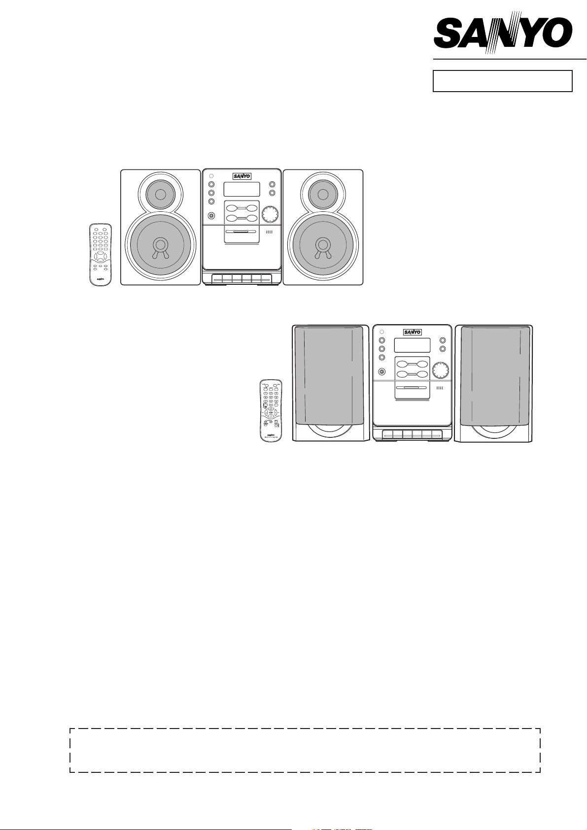
Service Manual
Micro Component System
(XE)
DC-DA1200M
DC-DA1250M
(XE-2)
(SP-2)
(SP)
Contents
Laser beam safety precaution .......................................... 1
Tape adjustments ............................................................ 1
Tuner adjustments ........................................................... 2
CD pick-up maintenance .................................................. 2
Exploded view .................................................................. 3
Parts list ........................................................................... 4
IC block diagram & description ........................................ 7
Schematic diagram
(FRONT) ...................................................................... 14
(CD) ............................................................................. 16
This service manual consists of
For XE-2 ; "DC-DA1200MU/XE-2" (Main unit : 129 693 13) and " SX-DA1200M/XE" (Speaker system: 165 104 04)
For SP-2 ; "DC-DA1250MU/SP-2" (Main unit : 129 693 16) and " SX-DA1250M/SP" (Speaker system: 165 045 15)
(TUNER) ...................................................................... 20
(AMPLIFIER) ............................................................... 24
Wiring diagram
(FRONT & CD) ............................................................ 18
(KEY) ........................................................................... 19
(TUNER) ...................................................................... 22
(AMPLIFIER) ............................................................... 26
(POWER TRANSFORMER) ........................................ 28
Wiring connection ............................................................ 29
PRODUCT CODE No.
129 694 13 (XE-2)
129 694 16 (SP-2)
REFERENCE No.
SM5810658
Page 2
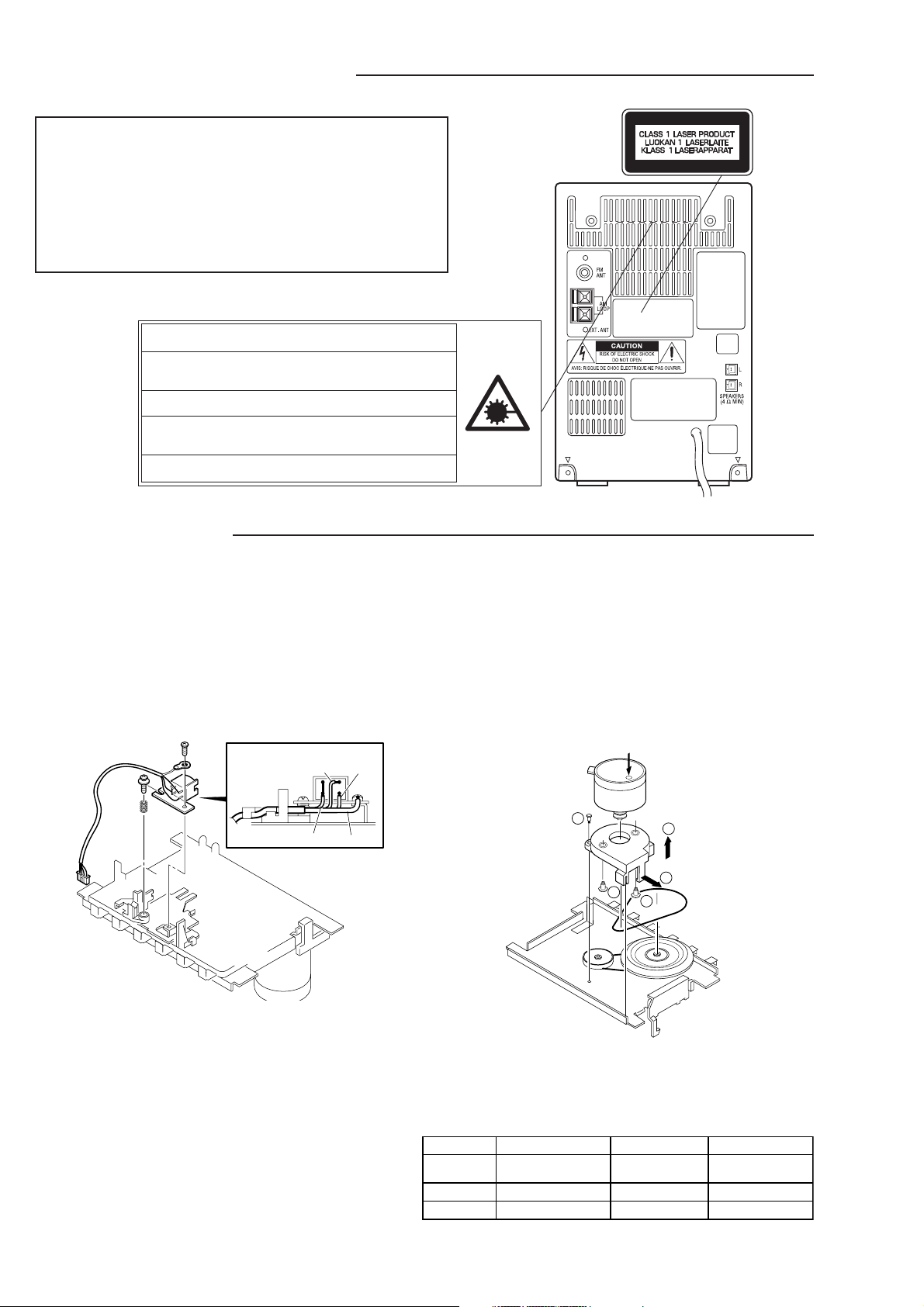
LASER BEAM SAFETY PRECAUTION
• Pick-up that emits a laser beam is used in this CD player section.
CAUTION :
THIS PRODUCT CONTAINS A LOW POWER LASER DEVICE,
TO ENSURE CONTINUED SAFETY DO NOT REMOVE ANY
COVERS OR ATTEMPT TO GAIN ACCESS TO THE INSIDE
OF THE PRODUCT.
REFER ALL SERVICING TO QUALIFIED PERSONNEL.
LASER OUTPUT ..............0.6 mW Max. (CW)
WAVELENGTH ..................790 nm
CAUTION – INVISIBLE LASER RADIATION WHEN OPEN AND
INTERLOCKS DEFEATED. AVOID EXPOSURE TO BEAM.
ADVARSEL – USYNLIG LASER STRÅLING VED ÅBNING, NÅR
SIKKERHEDSAFBRYDERE ER UDE AF FUNKTION, UNDGÅ UDS ÆTTELSE
FOR STRÅLING.
VARNING – OSYNLIG LASER STRÅLNING NÄR DENNA DEL ÄR ÖPPNAD
OCH SPÄRR ÄR URKOPPLAD. STRÅLEN ÄR FARLIG.
VORSICHT – UNSICHTBARE LASERSTRAHLUNG TRITT AUS, WENN
DECKEL GEÖFFNET UND WENN SICHERHEITSVERRIEGELUNG
ÜBERBRÜCKT IST. NICHT, DEM STRAHL AUSSETZEN.
VARO – AVATTAESSA JA SUOJALUKITUS OHITETTAESSA OLET ALTTIINA
NÄKYMÄTTÖMÄLLE LASERSÄTEILYLLE. ÄLÄ KATSO SÄ
TEESEEN.
TAPE ADJUSTMENTS
a. Replacing the head
1. After replacement, demagnetize the heads by using
a degausser.
2. Be sure to clean the heads before attempting to make
any adjustments.
3. Be sure both channels (1 and 2) are the same level.
(Using a dual-channels oscilloscope).
4. All wiring should be returned to the original position
after work is completed.
R / P HEAD
RED
WHITE
YELLOW EARTH
c. Adjusting motor speed
1. Insert the test tape (MTT-111 or etc. 3,000 Hz).
2. Press the PLAY button.
3. Use a flat-tip screwdriver to turn the SVR to adjust so
that the frequency counter becomes 3,000 Hz.
4. Press the STOP button.
d. Replacing the motor
MOTOR SPEED
ADJUSTMENT
1
4
3
2
4
b. Adjusting head azimuth
1. Load a test tape (VTT-738, etc. :10kHz) for
azimuth adjustment.
2. Press the PLAY button.
3. Use a cross-tip screwdriver to turn the screw for
normal azimuth adjustment so that the left and right
outputs are maximized at the same phase during
normal playback.
4. Press the STOP button.
e. Checking the mechanism torques
• Clean the head, capstan and pinch roller before making
any measurement.
Measurement Take-up torque Back tension Tape tension
Cassette for PLAY : TW-2111A PLAY : TW-2111A Drive-power cassette
measurement F.FWD/REW : TW-2231 TW-2412
PLAY 30 ~ 70gr.cm 1.0 ~ 6.0gr.cm 80 gr or more
F.FWD/REW 55 gr or more - -
- 1 -
Page 3
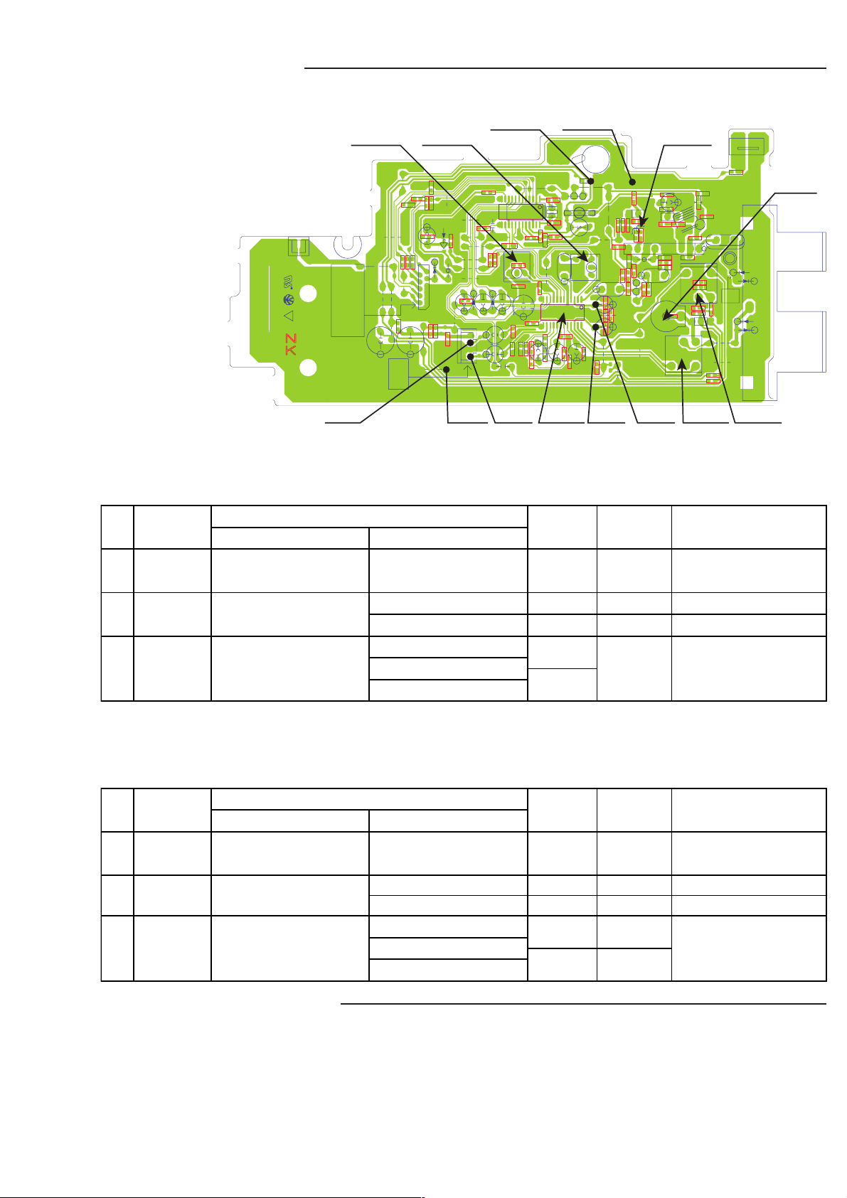
TUNER ADJUSTMENTS
C2152
C2107
R2103
R2107
C2110
C2141
C2323
C2310
C2318
C2308
R2312
R2308
R2309
C2309
C2115
R2302
C2304
C2312
R2306
R2455
R2110
R2109
• Use a plastic screw driver for adjustments.
• Speaker impedance : 4 ohms
• MODE : ST (Stereo)
• TUNING FM : 87.5 - 108MHz
AM : 522 - 1611 kHz
(9 kHz steps)
520 - 1610 kHz
(10 kHz steps)
CN204
TU_DATA
T002A 94V-0
1AD4B10D3000C
TP11
TP12
XF233 T2002 L2103
R2454
TU_D0
+5.6V
TU_CLK
GND
LID_SW
GND
KEY2
GND
TU_CE
J2203
J2304
J2310
C2903
J2311
J2106
+8.5V
TU_L
GND
TU-R
J2100
C2462
R2901
R2461
R2462
J2104
C2463
R2463
C2901
R2455
R2455
C2451
C2461
C2464
R2464
D2452
D2451
L2451
CN222
R2311
R2301
C2902
J2316
J2319
J2300
C2452
C2306
J2314
R2306
R2306
J2302
C2322
J2102
J2305
J2306
J2307
J2308
D2466
J2107
CN221
R2460
R2458
C2327
C2321
C2346
R2900
R2459
D2456
C2314
J2103
XF233
C2305
C2328
J2201
IC241
R2452
R2304
C2302
C2301
J2313
C2324
C2319
R2307
C2316
C2320
C2453
C2454
R2453
C2456
C2455
R2305
C2345
IC231
R2308
C2309
C2309
R2312
R2312R2308
R2309
R2309
C2307
J2309
X2451
C2315
C2317
Q2451
VT
VT
C2457
T2002
XF231
C2308
C2308
C2318
C2318
J2301
C2310
C2310
C2311
J2200
J2303
R2320
D2102
J2202
R2109
R2109
XF222
C2304
C2304
C2323
C2323
R2302
R2302
C2312
C2312
J2318
C2109
C2303
J2312
C2313
J2109
R2105
C2203
R2108
C2111
C2112
R2203R2202
R2106
L2103
R2107
C2110
R2107
C2110
IC211
L2104
R2205
XF221
E
R2201
R2204
Q2201
J2105
J2108
C2116
C2115
C2115
R2103
R2103
D2101
C2113
C2114
R2110
R2110
CT252
C2141
C2141
C2107R2102
C2107
C2101
L2151
C2104
L2001
C2105
L2153
R2131
C2154
R2149
C2151
D2153
J2101
R2101
C2103
R2151
R2148
XF211
D2103
D2104
C2152
C2152
D2151
D2152
J2315
J2317
S2001
R2910
CT252
CN201
CN202
1. FM
AdjustingCirc
Step
1
1
uit
IF Adjustment
Cover
FM Ant
SG=66dBuV
3 Tracking FM Ant
2. AM
AdjustingCirc
Step
uit
Antenna : 75Ω unbalanced direct, Modulation : 1 kHz
Dev. : ±22.5kHz(MONO), ±22.5kHz(STEREO),±6.75kHz(PILOT)
RF Level : dBuV EMF
Output Level : about 30mV at TP13, TP14, TP15
Connection
Input Output
IC231(3-22Pin)
TP24,25
---
TP11 (H)
TP12 (E)
TP13 (L)
TP15 (E)
Anntena : IRE Loop(SG), Moduration : 1kHz 30%
RF Level : dBuV EMF
Output Level : about 30mV at TP13, TP14, TP15
Connection
Input
Output
IC231 TP24TP25TP13TP15TP14
SG
Frequency
98.0MHz XF233
87.5MHz L2103
108.0MHz - - -
90.0MHz
106.0MHz
SG
Frequency
Adjustment
Adjustment
---
L2153L2151
Remark
Maximum
1.00±0.05V
5.3±0.50V Check Only
MaximumTP14 (R)
Remark
1
IF Adjustment
2
3 Loop Ant
CD PICK-UP MAINTENANCE
Cover
Voltage(MW)
Tracking
(MW)
Loop Ant -- -
---
About pick-up (Optical lens) Cleaning
TP12 (E)
TP13 (L)
TP14 (R)
TP15 (E)
450KHz
at 999kHz
522kHz TP11 (H)
1611kHz
603kHz
1404kHz
T2002
L2153
---
L2151
CT252
7.50±0.50V Check Only
Clean a lens with swab of the cotton which moistened it with alcohol, cleaning paper or cleaning disc appointed.
Specified cleaning disc : LC-1 (Part code : 645 026 1961 ..... manufactured by SANYO.)
Show a clean procedure in the following in reference by swab of cotton.
1. Cotton swab is wrapped with Cleaning paper.
2. Add the isopropyl alcohol.
3. Gently move the tip of cotton swab just like a draw a whirlpool from inside to outside on the surface of lens.
- 2 -
Maximum
1.00±0.05V
Maximum
Page 4
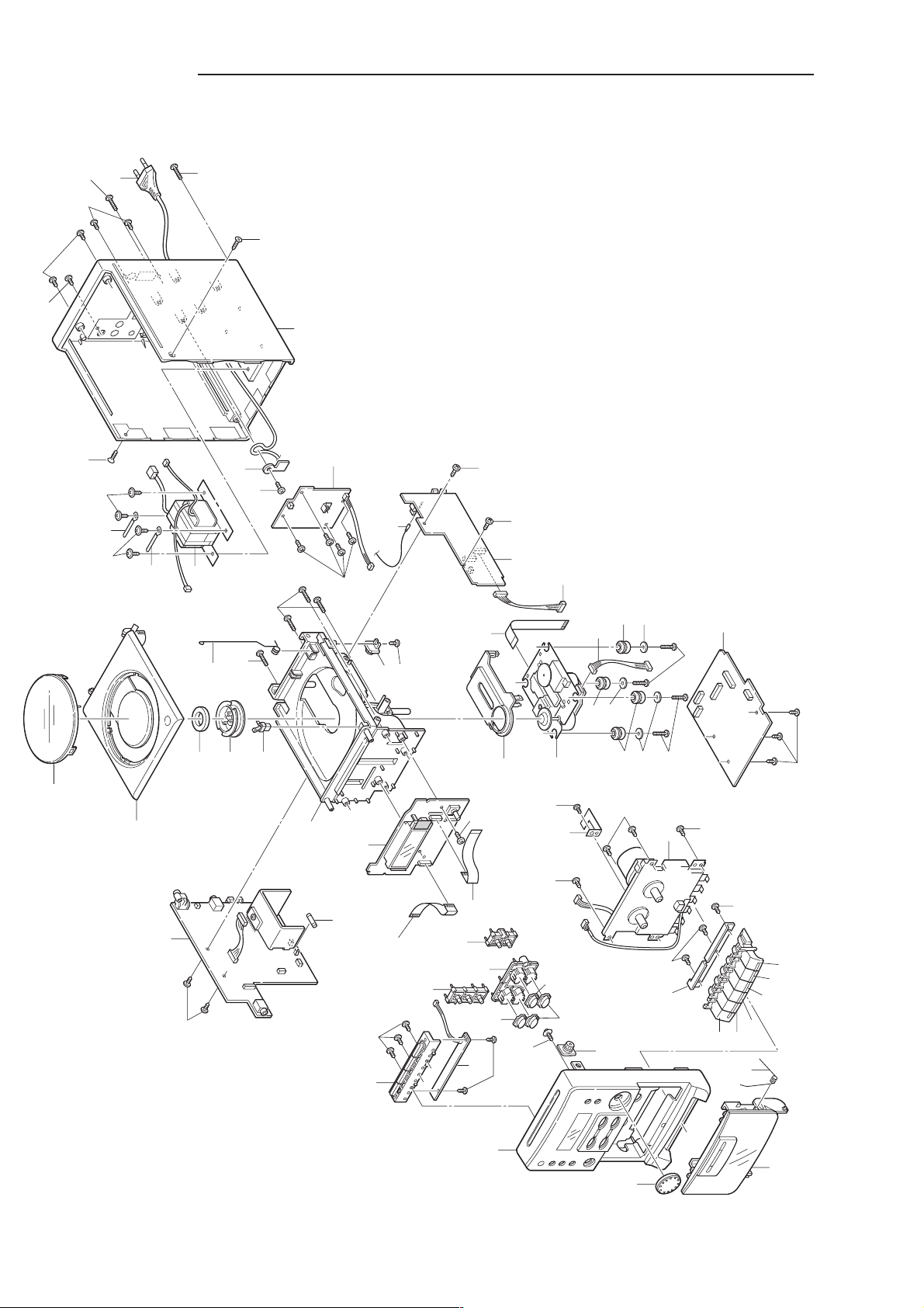
EXPLODED VIEW
20
33
19
10
9
12
25
26
27
28
30
31
N.S.P
32
29
6
8
7
11
22
2
13
14
15
17
18
16
3
4
5
1
23
51
21
21
21
54
55
24
Y03
Y01
Y02
Y05
Y05
Y04
Y04
Y05
Y06
Y07
53
56
52
Y11
Y11
Y12
Y14
Y13
Y15
Y16
Y16
Y17
Y17
Y20
Y20
Y22
Y22
Y21
Y19
Y19
Y18
Y13
Y08
Y09
Y10
Y10
Y10
Y09
72
71
73
74
75
76
58
59
57
This is a basic exploded view.
- 3 -
Page 5

PARTS LIST
PRODUCT SAFETY NOTICE
EACH PRECAUTION IN THIS MANUAL SHOULD BE FOLLOWED DURING SERVICING. COMPONENTS IDENTIFIED WITH THE
!!
IEC SYMBOL
PERFORMANCE CAN BE OF SPECIAL SIGNIFICANCE. WHEN REPLACING A COMPONENT IDENTIFIED BY
REPLACEMENT PARTS DESIGNATED, OR PARTS WITH THE SAME RATINGS OF RESISTANCE, WATTAGE OR VOLTAGE THAT
ARE DESIGNATED IN THE PARTS LIST IN THIS MANUAL. LEAKAGE-CURRENT OR RESISTANCE MEASUREMENTS MUST BE
MADE TO DETERMINE THAT EXPOSED PARTS ARE ACCEPTABLY INSULATED FROM THE SUPPLY CIRCUIT BEFORE
RETURNING THE PRODUCT TO THE CUSTOMER.
CAUTION : Regular type resistors and capacitors are not listed. To know those values, refer to the schematic diagram.
N.S.P : Not available as service parts.
PACKING & ACCESSORIES
REF.NO. PART NO. DESCRIPTION
CABINET & CHASSIS
REF.NO. PART NO. DESCRIPTION
1 614 330 7648 ASSY,DOOR,DECK
2 614 329 2449 SPRING,DOOR DECK
3 614 329 2258 KNOB,VOLUME
4 614 330 7662 ASSY,PANEL FRONT
5 614 309 7969 ASSY,GEAR,CASSETTE
6 614 329 2210 DEC,WINDOW BUTTON
7 614 329 6690 DEC,WINDOW BUTTON
8 614 329 6706 DEC,WINDOW BUTTON
9 614 329 2142 BUTTON,TOP,4 KEYS
10 614 329 2159 BUTTON,LEFT,3 KEYS
11 614 329 2135 BUTTON,FUNC,4 KEYS
12 614 329 2166 BUTTON,RIGHT,2 KEYS
13 614 329 2265 KNOB,DECK MECHA,REC
14 614 329 2272 KNOB,DECK MECHA,PLAY
15 614 329 2289 KNOB,DECK MECHA,REW
16 614 329 2296 KNOB,DECK MECHA,FFWD
17 614 329 2302 KNOB,DECK MECHA,STOP/EJECT
18 614 329 2319 KNOB,DECK MECHA,PAUSE
19 614 329 2340 MOUNTING,DECK MECHA
20 614 308 0534 SPRING,PLATE,REC
21 614 310 3899 SPACER,MECHA,CD+DA11
22 614 325 6014 ASSY,MECHA,DA11T3CN-SASH
23 614 307 2072 COVER,PICK-UP
24 614 322 2132 ASSY,GEAR,LID,CD
25 614 329 2357 MOUNTING,CD
26 614 303 0263 LATCH,PUSH,CD DOOR LOCKING
27 614 307 8821 PULLEY
28 614 303 0256 LATCH,MAGNET
29 614 329 2456 SPRING,DOOR CD
30 614 329 2333 LID,CD
31 614 329 2234 DEC,WINDOW CD
32 614 332 1613 ASSY,CABINET,REAR(For XE)
32 614 332 2085 ASSY,CABINET,REAR(For SP)
33 614 309 7976 ASSY,MECHA,TM-DA70TN-SH
!
IN THE PARTS LIST AND THE SCHEMATIC DIAGRAM DESIGNATED COMPONENTS IN WHICH SAFETY AND
!!
!
, USE ONLY THE
Regular type resistors are less than 1/4 W carbon type and 0 ohm chip resistors.
Regular type capacitors are less than 50 V and less than 1000 µF type of Ceramic type and Electrical type.
FIXING PARTS
REF.NO. PART NO. DESCRIPTION
614 332 1682 CARTON CASE(For XE)
614 332 2146 CARTON CASE(For SP)
614 329 2494 CUSHION,REAR
614 329 2487 CUSHION,FRONT
614 332 1699 INSTRUCTION MANUAL(For XE)
614 332 2153 INSTRUCTION MANUAL(For SP)
614 332 2160 INSTRUCTION SHEET,
GREECE(For XE)
614 332 2177 INSTRUCTION SHEET,
GREECE(For SP)
645 046 8322 ASSY,ANTENNA,LOOP
645 072 9904 REMOCON,RB-DA1200M2
614 330 8898 LID,BATTERY REMOCON,SERVICE
614 330 8270 ASSY,BOX,SPEAKER(For XE)
614 331 7036 ASSY,BOX,SPEAKER(For SP)
Y01 411 187 2709 SCR S-TPG BIN 2.3X6,
BUTTON TOP+PWB TOP
Y02 411 021 6405 SCR S-TPG BIN 3X8,
BUTTON TOP+PANEL FRONT
Y03 411 020 8905 SCR S-TPG BRZ+FLG 3X10,GEAR
Y04 411 021 3503 SCR S-TPG BIN 3X10,
PANEL+MTG DECK KNOB
Y05 411 021 3503 SCR S-TPG BIN 3X10,
PANEL+DECK MECHA
Y06 411 126 1404 SCR S-TPG BIN 2X4,
SPRING DECK REC
Y07 411 021 3503 SCR S-TPG BIN 3X10,
FRONT PWB+MOUNT
Y08 411 021 3503 SCR S-TPG BIN 3X10,
MTG CD+CD PCB
Y09 411 021 1806 SCR S-TPG BIN 2.6X10,
MTG CD+MECHA CD
Y10 411 092 0906 WASHER Z 2.6X10X0.5,
MECHA,CD+MOUNTING
Y11 411 021 6405 SCR S-TPG BIN 3X8,
MTG CD+TUNER PCB
Y12 411 021 3503 SCR S-TPG BIN 3X10,
MTG CD+ASSY,GEAR
Y13 411 021 4906 SCR S-TPG BIN 3X20,
PANEL+MOUNTING
Y14 411 021 3503 SCR S-TPG BIN 3X10,
MTG CD+AMP PCB
Y15 411 021 3503 SCR S-TPG BIN 3X10,
REAR+PWB POWER
Y16 411 020 9100 SCR S-TPG BRZ+FLG 3X12,
REAR+P-TRANS
Y17 614 130 0382 LUG,FOR PT
Y18 411 021 3503 SCR S-TPG BIN 3X10,
REAR+STOPPER
Y19 411 098 7800 SCR S-TPG FLT 3X12,
PANEL+REAR+MOUNTING
Y20 411 021 4500 SCR S-TPG BIN 3X16,PANEL+REAR
Y21 411 021 3503 SCR S-TPG BIN 3X10,
MTG CD+REAR
Y22 411 021 3503 SCR S-TPG BIN 3X10,
C-REAR(ANT TERMINAL)
ELECTRICAL PARTS
REF.NO. PART NO. DESCRIPTION
51 423 016 7908 FUSE 250V 2.5A
52 614 327 0812 FLEXIBLE FLAT CABLE,
FRONT TO AMP
53 614 332 1880 FLEXIBLE FLAT CABLE,
TUNER TO FRONT
54 614 332 1873 ASSY,WIRE,CD CD MECHA
55 614 332 1866 ASSY,WIRE,CD TO TUNER
56 614 332 6656 FLEXIBLE FLAT CABLE,
CD PICK UP(For XE)
56 614 328 4376 FLEXIBLE FLAT CABLE,
(For details to page 7)
57 614 274 2013 CORD,ID CONNECTOR,FM ANT
58 645 066 5646 TRANS,POWER
59 645 016 9939 CORD,POWER-1.74MK
- 4 -
CD PICK UP(For SP)
Page 6

PARTS LIST
KEY P.W.BOARD ASSY
REF.NO. PART NO. DESCRIPTION
71 614 331 7111 ASSY,PWB,KEY(Only initial)
CN605 614 330 3367 ASSY,WIRE,KEY TO TUNER
S6512 614 220 5471 SWITCH,TACT
or 645 006 5958 SWITCH,PUSH 1P-1T
or 614 240 1002 SWITCH,TACT
S6513 645 006 5958 SWITCH,PUSH 1P-1T
or 614 240 1002 SWITCH,TACT
or 614 220 5471 SWITCH,TACT
S6514 614 220 5471 SWITCH,TACT
or 614 240 1002 SWITCH,TACT
or 645 006 5958 SWITCH,PUSH 1P-1T
S6515 614 220 5471 SWITCH,TACT
or 614 240 1002 SWITCH,TACT
or 645 006 5958 SWITCH,PUSH 1P-1T
FRONT P.W.BOARD ASSY
REF.NO. PART NO. DESCRIPTION
72 614 331 7128 ASSY,PWB,FRONT(Only initial)
AH601 614 331 7203 HOLDER,LCD
AH602 614 329 2180 COVER,LED
AR601 614 329 2395 REFLECTOR,LCD
BR602 614 328 4543 HOLDER,LED
CN601 645 059 0474 SOCKET,FPC 14P,FRONT-AMP
CN602 645 072 1946 SOCKET,FPC 10P,FRONT-TU
D6010 407 012 4406 DIODE 1SS133
D6110 407 012 4406 DIODE 1SS133
D6111 407 012 4406 DIODE 1SS133
D6112 407 012 4406 DIODE 1SS133
D6115 407 099 4603 ZENER DIODE MTZJ3.9B
D6201 407 241 2204 LED LT7V34-81-UR91
D6202 407 241 2204 LED LT7V34-81-UR91
DS601 407 217 1101 PHOTO DIODE SPS-442-1G
or 407 229 6101 PHOTO DIODE SPS-442-1-G1
IC601 410 545 7400 IC LC877148A-54K7-E,MICON
L6010 645 001 5441 INDUCTOR,2.2U K
LCD61 645 072 1960 LCD
LS601 614 329 6720 DEC,SHEET LCD,DEC-LCD-SHEET
Q6101 405 014 4509 TR 2SC2412K-R
or 405 011 1006 TR 2SC1623-L6
or 405 146 2206 TR KTC3875-GR
Q6107 405 005 5508 TR 2SA812-M6
or 405 002 0308 TR 2SA1037K-R
or 405 146 9700 TR KTA1504-GR
Q6108 405 011 1006 TR 2SC1623-L6
or 405 014 4509 TR 2SC2412K-R
or 405 146 2206 TR KTC3875-GR
S6001 645 057 4689 SWITCH,ROTARY(ENCODER)
S6500 614 220 5471 SWITCH,TACT
or 614 240 1002 SWITCH,TACT
or 645 006 5958 SWITCH,PUSH 1P-1T
S6501 614 220 5471 SWITCH,TACT
or 614 240 1002 SWITCH,TACT
or 645 006 5958 SWITCH,PUSH 1P-1T
S6502 614 220 5471 SWITCH,TACT
or 614 240 1002 SWITCH,TACT
or 645 006 5958 SWITCH,PUSH 1P-1T
S6503 614 220 5471 SWITCH,TACT
or 614 240 1002 SWITCH,TACT
or 645 006 5958 SWITCH,PUSH 1P-1T
S6504 614 240 1002 SWITCH,TACT
or 645 006 5958 SWITCH,PUSH 1P-1T
or 614 220 5471 SWITCH,TACT
S6505 614 220 5471 SWITCH,TACT
or 614 240 1002 SWITCH,TACT
or 645 006 5958 SWITCH,PUSH 1P-1T
S6506 614 220 5471 SWITCH,TACT
or 614 240 1002 SWITCH,TACT
or 645 006 5958 SWITCH,PUSH 1P-1T
S6510 614 220 5471 SWITCH,TACT
or 614 240 1002 SWITCH,TACT
or 645 006 5958 SWITCH,PUSH 1P-1T
REF.NO. PART NO. DESCRIPTION
S6511 614 220 5471 SWITCH,TACT
or 614 240 1002 SWITCH,TACT
or 645 006 5958 SWITCH,PUSH 1P-1T
X6101 645 032 1627 OSC,CRYSTAL 32.768KHZ
X6102 645 057 1138 OSC,CERAMIC 6.0MHZ
or 645 018 6103 OSC,CERAMIC 6.000MHZ
CD P.W.BOARD ASSY
REF.NO. PART NO. DESCRIPTION
73 614 331 7135 ASSY,PWB,CD(Only initial)
CN111 645 059 0498 SOCKET,FPC 16P
CN112 645 005 8127 PLUG,6P
or 614 310 2472 PLUG,6P
CN122 645 005 8134 PLUG,8P
or 614 310 2496 PLUG,8P
CN123 645 005 8110 PLUG,4P
or 614 310 2458 PLUG,4P
CN164 645 005 8127 PLUG,6P
or 614 310 2472 PLUG,6P
D1501 407 098 3300 DIODE RL153-BF-S2
D1502 407 098 3300 DIODE RL153-BF-S2
D1503 407 098 3300 DIODE RL153-BF-S2
IC101 410 538 0401 IC LC78646E-UHK-E
IC102 410 538 0500 IC LC78684NE-UHK-E
IC103 410 530 7804 IC M12L16161A-7TG
IC104 409 582 6002 IC LA6548NH-E
L1301 645 002 1459 INDUCTOR,22U K
L1302 645 037 2858 CORE,PIPE
L1303 645 001 4581 INDUCTOR,100U K
L1401 645 037 2858 CORE,PIPE
PR151 645 066 9668 PROTECTOR,0.4A 125V
Q1301 405 008 7301 TR 2SB810-F
or 405 008 7202 TR 2SB810-E
or 405 008 6809 TR 2SB808-F-SPA
Q1401 405 017 9600 TR 2SC3330-T
or 405 011 8609 TR 2SC1740S-S
or 405 011 8500 TR 2SC1740S-R
or 405 143 8706 TR KTC3199-GR
or 405 017 9709 TR 2SC3330-U
Q1501 405 009 5306 TR 2SB927-T
or 405 009 5207 TR 2SB927-S
or 405 141 3604 TR KTA1273-Y
X1451 645 020 9024 OSC,CRYSTAL 16.9344MHZ
TUNER P.W.BOARD ASSY
REF.NO. PART NO. DESCRIPTION
74 614 331 7104 ASSY,PWB,TUNER(Only initial)
C2457 403 259 0508 NP-ELECT 1U M 50V
CN201 614 221 8273 TERMINAL
CN202 645 025 4703 TERMINAL,ANTENNA
or 645 038 7715 TERMINAL
CN204 614 310 2434 PLUG,2P
or 645 005 7366 PLUG,2P
CN221 614 310 2458 PLUG,4P
or 645 005 8110 PLUG,4P
CN222 645 072 1946 SOCKET,FPC 10P
CT252 645 032 5663 TRIMMER,7PF
D2101 407 157 8109 VARACTOR DI SVC211-B
D2102 407 157 8109 VARACTOR DI SVC211-B
D2103 407 012 4406 DIODE 1SS133
D2104 407 012 4406 DIODE 1SS133
D2151 407 012 4406 DIODE 1SS133
D2152 407 012 4406 DIODE 1SS133
D2153 407 105 1305 VARACTOR DI SVC342L-V
or 407 105 1602 VARACTOR DI SVC342M-V
D2451 407 012 4406 DIODE 1SS133
D2452 407 153 7502 ZENER DIODE GZS3.0B
D2456 407 012 4406 DIODE 1SS133
D2466 407 012 4406 DIODE 1SS133
- 5 -
Page 7
PARTS LIST
REF.NO. PART NO. DESCRIPTION REF.NO. PART NO. DESCRIPTION
IC211 409 016 0200 IC LA1186N-AUDIO
IC231 409 474 3201 IC LA1844ML
IC241 409 439 4502 IC LC72121M-D
L2001 645 040 2753 INDUCTOR,AIR —
L2103 645 040 2746 COIL,AIR —
L2104 645 002 1534 INDUCTOR,8.2U K
L2151 645 037 2377 TRANS,ANT,796KHZ
L2153 645 040 2739 TRANS,OSC,796KHZ
L2451 645 031 7842 INDUCTOR,100U K
or 645 001 4581 INDUCTOR,100U K
Q2201 405 151 4301 TR KTC3195-Y
or 405 151 4806 TR KTC3195-O
Q2451 405 036 3702 TR 2SA1564
or 405 151 5209 TR KRA107M
or 405 000 0904 TR DTA114YS
or 405 078 2404 TR BN1A4P
S2001 645 023 5795 SWITCH,LEVER
T2002 645 046 2023 FILTER,450KHZ
X2451 645 023 4965 OSC,CRYSTAL 7.2MHZ
XF211 614 252 1045 FILTER,LC
or 645 026 2975 FILTER,BP 108MHZ
or 645 059 0047 FILTER,BP
XF221 645 054 1223 CERAMIC FILTER 10.70MHZ
or 645 010 7665 CERAMIC FILTER 10.70MHZ
or 614 240 2917 FILTER,CERAM
XF222 645 054 1223 CERAMIC FILTER 10.70MHZ
or 645 010 7665 CERAMIC FILTER 10.70MHZ
or 614 240 2917 FILTER,CERAM
XF231 645 059 0054 CERAMIC FILTER 450KHZ
or 645 041 9324 CERAMIC FILTER 450KHZ
XF233 645 039 9923 TRANS,IF 10.7MHZ
or 645 040 9981 TRANS,IF 10.7MHZ
AMPLIFIER P.W.BOARD ASSY
REF.NO. PART NO. DESCRIPTION
75 614 331 7081 ASSY,PWB,AMP(Only initial)
C4714 403 058 4608 POLYESTER 0.15U J 50V
C4814 403 058 4608 POLYESTER 0.15U J 50V
C4913 403 329 6003 ELECT 4700U M 25V
C4918 403 377 6307 POLYESTER 1000P J 50V
or 403 056 7502 POLYESTER 1000P J 50V
CN401 645 006 1875 PLUG,2P,SPEAKER
CN402 645 006 1875 PLUG,2P,SPEAKER
CN405 645 004 2904 PLUG,4P
or 614 310 2755 PLUG,4P
CN406 645 005 8110 PLUG,4P
or 614 310 2458 PLUG,4P
CN411 645 004 2881 PLUG,2P,POWER
or 614 310 2731 PLUG,2P,POWER
CN421 645 055 1017 JACK,PHONE D3.6,HEADPHONE
or 645 011 6384 JACK,PHONE D3.6,HEADPHONE
CN491 645 059 0474 SOCKET,FPC 14P,FRONT-AMP
CN492 614 330 8720 ASSY,WIRE
D4102 407 012 4406 DIODE 1SS133
D4951 407 099 6003 ZENER DIODE MTZJ9.1B
D4953 407 012 4406 DIODE 1SS133
D4961 407 012 4406 DIODE 1SS133
D4962 407 012 4406 DIODE 1SS133
D4963 407 012 4406 DIODE 1SS133
D4980 407 098 3300 DIODE RL153-BF-S2
D4981 407 098 3300 DIODE RL153-BF-S2
D4982 407 098 3300 DIODE RL153-BF-S2
D4983 407 098 3300 DIODE RL153-BF-S2
D4984 407 098 3300 DIODE RL153-BF-S2
D4993 407 012 4406 DIODE 1SS133
FCL41 645 006 4760 HOLDER,FUSE
or 645 031 7903 HOLDER,FUSE
FCL42 645 006 4760 HOLDER,FUSE
or 645 031 7903 HOLDER,FUSE
HS401 614 332 1514 HEAT SINK
IC410 409 384 3506 IC BA3314F
IC411 409 614 0701 IC LC75348M-E
IC412 409 612 2202 IC KIA6282K
IC446 409 039 9204 IC NJM78L05A
L4781 645 002 1459 INDUCTOR,22U K
L4881 645 002 1459 INDUCTOR,22U K
L4902 645 031 5893 TRANS,OSC,85KHZ,O.S.C
PR495 645 066 9743 PROTECTOR,1.5A 125V
PR496 645 066 9743 PROTECTOR,1.5A 125V
Q4104 405 109 9204 TR KRC102M-A
or 405 000 3103 TR DTC114ES
Q4106 405 000 3103 TR DTC114ES
or 405 109 9204 TR KRC102M-A
Q4320 405 143 8706 TR KTC3199-GR
or 405 017 9600 TR 2SC3330-T
or 405 017 9709 TR 2SC3330-U
or 405 011 8500 TR 2SC1740S-R
or 405 011 8609 TR 2SC1740S-S
Q4321 405 004 5004 TR 2SA608-G-NP
or 405 004 4502 TR 2SA608-F-NP
or 405 141 3505 TR KTA1266-Y
or 405 141 3406 TR KTA1266-GR
Q4740 405 109 9204 TR KRC102M-A
or 405 000 3103 TR DTC114ES
Q4751 405 151 4400 TR KTD1303
or 405 021 0204 TR 2SD1012-F-SPA
or 405 021 0600 TR 2SD1012-G-SPA
or 405 033 6706 TR 2SD1468S-R
or 405 033 6805 TR 2SD1468S-S
Q4840 405 000 3103 TR DTC114ES
or 405 109 9204 TR KRC102M-A
Q4851 405 151 4400 TR KTD1303
or 405 021 0204 TR 2SD1012-F-SPA
or 405 021 0600 TR 2SD1012-G-SPA
or 405 033 6706 TR 2SD1468S-R
or 405 033 6805 TR 2SD1468S-S
Q4902 405 017 9709 TR 2SC3330-U
or 405 017 9600 TR 2SC3330-T
or 405 011 8609 TR 2SC1740S-S
or 405 011 8500 TR 2SC1740S-R
or 405 143 8706 TR KTC3199-GR
Q4904 405 017 9709 TR 2SC3330-U
or 405 017 9600 TR 2SC3330-T
or 405 011 8609 TR 2SC1740S-S
or 405 011 8500 TR 2SC1740S-R
or 405 143 8706 TR KTC3199-GR
Q4951 405 095 1701 TR 2SD2061-F
or 405 095 1602 TR 2SD2061-E
or 405 138 6403 TR KTD2058Y
or 405 158 2102 TR KTC2026-Y
Q4992 405 008 2504 TR 2SB698-G
or 405 008 2405 TR 2SB698-F
or 405 141 3703 TR KTA1271-Y
Q4994 405 000 3806 TR DTC114YS
or 405 143 0007 TR KRC107M
Q4995 405 141 3703 TR KTA1271-Y
or 405 008 2405 TR 2SB698-F
or 405 008 2504 TR 2SB698-G
Q4996 405 143 8706 TR KTC3199-GR
or 405 017 9600 TR 2SC3330-T
or 405 017 9709 TR 2SC3330-U
or 405 011 8500 TR 2SC1740S-R
or 405 011 8609 TR 2SC1740S-S
Q4997 405 143 8706 TR KTC3199-GR
or 405 017 9600 TR 2SC3330-T
or 405 017 9709 TR 2SC3330-U
or 405 011 8500 TR 2SC1740S-R
or 405 011 8609 TR 2SC1740S-S
R4752 402 071 1304 FUSIBLE RES 2.2 JA 1/4W
R4852 402 071 1304 FUSIBLE RES 2.2 JA 1/4W
R4941 401 121 8607 MT-FILM 27 FD 1/4W
S4950 645 038 7586 SWITCH,PUSH,R/PSW
SA401 411 021 6405 SCR S-TPG BIN 3X8
SA402 411 021 6405 SCR S-TPG BIN 3X8
- 6 -
Page 8

PARTS LIST
POWER TRANSFORMER P.W.BOARD ASSY
REF.NO. PART NO. DESCRIPTION
76 614 331 7098 ASSY,PWB,DG(Only initial)
CN451 614 017 8203 TERMINAL BOARD
CN452 614 017 8203 TERMINAL BOARD
CN455 645 005 9315 PLUG,2P
L4591 645 038 6053 INDUCTOR,181U
IC BLOCK DIAGRAM & DESCRIPTION
IC101 LC78646-UHK-E (CMOS LSI for CD Player)
PDO1
PCKIST
VVSS
CONT4
CONT5
PDO2
SBCK/FG
SBCK/CONT6
FR
LDD
1 60
SLCO
2
SLCIST
3
EFMIN
4
RF
5
RFVDD
6
RFVSS
7
FIN1
8
FIN2
9
TIN1
10
TIN2
11
VREF
12
REFI
13
FE
14
TEC
15
TE
16
RFMON
17
JITTC
18
ADAVDD
19
ADAVSS
20
TDO
21 80
FDO
Pin
Pin Name
No.
1 SLCO O 2 SLCIST AI - SLCO output current adjustment resistor connection pin.
3 EFMIN I - RF signal input pin.
4 RF AO - RF monitor pin.
5 RFVDD - - RF power supply pin.
6 RFVSS - - RF ground pin. Must be connected to 0V.
7 FIN1 AI - A+C signal input pin.
8 FIN2 AI - B+D signal input pin.
9 TIN1 AI - E signal input pin.
10 TIN2 AI F signal input pin.
11 VREF AO RFVDD/2 VREF voltage output pin.
12 REFI AI - Reference voltage seting pin.
13 FE AO ZHI FE signal monitor pin.
14 TEC AO - TE signal LPF capacitor connection pin.
15 TE AO ZHI TE signal monitor pin.
16 RFMON AO ZHI RF internal signal monitor pin.
17 JITTC A - Jitter detection capasitor connection pin.
18 ADAVDD - - Servo A/D, D/A supply pin.
19 ADAVSS - - Servo A/D, D/A ground pin. Must be connected to 0V.
20 TDO AO ADAVDD/2 Tracking control output pin. D/A output.
21 FDO AO ADAVDD/2 Focus control output pin. D/A output.
22 SPDO AO ADAVDD/2 Spindle control output pin. D/A output.
23 SPDO AO ADAVDD/2 Thread control output pin. D/A output.
24 GPDAC AO ADAVDD/2 Servo D/A general-purpose output pin.
25 CONT4 I/O Input mode
26 CONT5 I/O Input mode
27 SBCK/CONT6 I/O Input mode
28 SBCK/FG I -
29 DEFECT O L Defect pin.
30 V / *P O H
31 FSEQ O L
32 MONI 1 O L Internalsignal monitor pin 1.
33 MONI 2 O L Internalsignal monitor pin 2.
34 MONI 3 O L Internalsignal monitor pin 3.
35 MONI 4 O L Internalsignal monitor pin 4.
36 MONI 5 O L Internalsignal monitor pin 5.
37 (3.3V)VSS - -
Reset
I/O
state
Control output.
Slice level
control
General-purpose
input / output pin 4.
General-purpose
input / output pin 5.
General-purpose
input / output pin 6,
or subcode read clock input pin.
Subcode read clock input pin / FG signal input pin /
external emphasis setting pin.
Set to command pin function. Must be connected to 0V.
Rough servo / phase control automatic switching monitor
output pin.
"H" for rough servo and "L" for phase servo.
Synchronization signal detection output pin.
Outputs a high level when the synchronization signal
detected
from the EFM signal and the internally generated
synchronization
signal agree.
Digital ground pin. Must be connected to 0V.
VVDD
LDS
22792378247725762675277428732972307131703269336834673566366537643863396240 61
SLDO
SPDO
GPDAC
Function description
Controlled by commands
from the microprocessor.
Any of these that are unused
must be either set up as input
pin ports and connected to 0V,
or set up as output pin ports
and left open.
TAPE MECHANISM
REF.NO. PART NO. DESCRIPTION
33 614 309 7976 ASSY,MECHA,TM-DA70TN-SH
614 312 0629 ASSY,MOTOR,FOR SERVICE
645 009 1612 PINCH ROLLER ARM ASSY
645 009 1766 RF BELT
645 033 3415 MAIN BELT
645 041 3025 R.P HEAD
645 033 8625 E HEAD 6PA
or 645 072 9775 E HEAD TC-238
*RES
CONT3
VSS
FSEQ
MONI 1
Pin Name
VDD5V
MONI 2
CONT1
CONT2
V / *P
DEFECT
Pin
No.
38 VDD - - Digital power supply pin.
39 DOUT O L Digital OUT output pin.
40 TEST I L Test input pin. Must be connected to 0V.
41 LVDD - 42 LCHO AO LVDD/2 L channel output pin.
43 LVSS - - L channel ground pin. Must be connected to 0V.
44 RVSS - 45 RCHO AO LVDD/2 R channel output pin.
46 RVDD - - R channel power supply pin.
47 XVDD - 48 XOUT O Oscillator Connections for a 33.8688MHz or 16.9344MHz
49 XIN I Oscillator crystal oscillator pin.
50 FSX/16MIN I/O Input mode
51 XVSS - - Crystal oscillator Crystal oscillator ground pin. Must be connected to 0V.
52 C2F O H C2 flag output pin.
53 EFLG O L C1, C2 error correction monitor pin.
54 16MOUT O CLK output 16.9344MHz output pin.
55 ASLRCK I
56 ASDACK I Bit clock input pin. (Must be connected to 0V when unused)
57 ASDFIN I
58 LRSY O L
59 DATACK O L Bit clock output pin.
60 DATA O L L/R channel data output pin.
61 CE I 62 CL I - Data transfer clock input pin.
63 DI I - Data input pin.
64 DO O (H) Data output pin. (Nch open drain output)
65 *WRQ O H Interruption signal output pin.
66 *RES I 67 DRF O L Focus ON detect pin.
68 VDD5V - - Microprocessor interface power supply pin.
69 VSS - - Digital ground pin. Must be connected to 0V.
70 CONT3 I/O Input mode General-purpose output pin 3. Controlled by commands from the microprocessor.
71 CONT2 I/O Input mode General-purpose output pin 2. Must be set as an input pin and connected to 0V
72 CONT1 I/O Input mode General-purpose output pin 1. or set as an output pin and left open when unused.
73 PDO1 O
74 PDO2 O Input mode Phase comparison output pin 2 to control built-in VCO.
75 VVSS - - Built-in VCO GND pin. Must always be connected to 0V.
76 PCKIST AI - Resistor connection pin to set current for PD01 and 02 outputs.
77 VVDD - - Built-in VCO power supply pin.
78 FR AI - Resistor connection pin to set the frequency range of built-in VCO.
79 LDS AI - Laser power detection signal input pin.
80 LDD AO - Laser power detection signal output pin.
Note) The same potential must be supplied to all power supply pins, i. e. , RFVDD, VVDD, ADAVDD, VDD, LVDD,
RVDD AND XVDD. Pins operated from the microprocessor interface power supply (VDD5V) pin :
CE(61 pin), CL(62pin), DI(63 pin), DO(64 pin), *WRQ(65 pin), RES(66 pin), DRF(67 pin), CONT1(72 pin),
CONT2(71 pin), CONT3(70 pin)
*WRQ
DRF
MONI 3
MONI 4
MONI 5
Reset
I/O Function description
state
- 7 -
CL
CE
DI
DO
DATA
59
DATACK
58
LRSY
57
ASDFIN
56
ASDACK
55
ASLRCK
54
16MOUT
53
EFLG
52
C2F
51
XVSS
50
FSX/16MIN
49
XIN
48
XOUT
47
XVDD
46
RVDD
45
RCHO
44
RVSS
43
LV SS
42
LCHO
41
LV DD
VDD
TEST
DOUT
(3.3V)VSS
L channel D/A converter
R channel D/A converter
Crystal oscillator
7.35kHz synchronization signal output pin.
DF, DAC external clock input pin.
Antishock mode
Digital data output
Micro
-processor
interface
Reset input pin.
This pin must be set low briefly after power is first applied.
Phase comparison output pin 1 to control built-in VCO.
PLL
L channel power supply pin.
R channel ground pin. Must be connected to 0V.
Crystal oscillator power supply pin.
L/R clock input pin. (Must be connected to 0V when unused)
L/R channel data input pin.
(Must be connected to 0V when unused)
L/R clock output pin.
Chip enable signal input pin.
Page 9

IC BLOCK DIAGRAM & DESCRIPTION
IC101 LC78646-UHK-E (CMOS LSI for CD Player)
FE
TE
TEC
RF
FIN1
FIN2
TIN1
TIN2
REFI
DEFECT
ADIN
ADAVDD
ADAVSS
JITTC
SLCO
EFMIN
SLCIST
PCK
PDO1
PDO2
FR
PCKIST
VVDD
VVSS
SBCK/FG
+
+
+
+
-
TBAL
TBAL
LEVEL SET
A/D
SLICE LEVEL
CONTROL
PLL
VCEC
MIX
+
+
LPF
+
+
-
RAM
SERVO
PROCESSEROR
JITTER
DETECT
CLV,CAV
CONTROL
EQ
AGC
LPF
LPF
+
SW
+
-
TRACK JUMP
AUTO ADJUST
SW
D/A
DRF
RUPTURE DEFECT
FRAME SYNC
DETECT,PROTECT INSERT
EFM DECODE
PH
BH
+
-
+
-
MONI
CONT
APC
S/H
VDD5V
RFVDD
RFVSS
RFMON
VREF
LDD
LDS
FDO
TDO
SLDO
SPDO
GPDAC
DRF
FSEQ
V / *P
XIN
XOUT
16MOUT
XVDD
XVSS
*RES
*WRQ
CL
CE
DI
DO
VDD5V
CONT1,2,3
CONT4,5,
SBCK/CONT6
TEST
CLOCK
GENERATOR
COMMAND
INTERFACE
GENERAL-PURPOSE
PORTS
8FS
DIGITAL FILTER
1bit DAC
SUBCODE DECODE CRC
MONITOR SIGNAL SELECTOR
ERROR
CORRECTION
AUDIO CD
C1-2,C2-2
INTERPOLATION
MUTE
ATTENUATION
DEEMPHASIS
LPF
LVSS
LVDD
LCHO
RCHO
RVSS
RVDD
RAM
AUDIO OUT
SERIAL
OUT
EXTERNAL
AUDIO
VDD
VSS
MONI 1~5
FSX/16MIN
C2F
EFLG
DOUT
LRSY
DATACK
DATA
ASLRCK
ASDACK
ASDFIN
- 8 -
Page 10

IC BLOCK DIAGRAM & DESCRIPTION
IC102 LC78684NE-UHK-E (MP3 Decoder for CD Player)
CASUB
CASLB
WEB
OEB
MADRS[12:0]
MDATA[15:0]
RASB
CL
CMDIN
CE
CMDOUT
INTB
System
CKIN
VPRER
VCOC
VPDO
CKOUT
WOK
CNTOK
OVF
LRSY
DATACK
DATAIN
C2FIN
SFSY
PW
SBSY
SBCK
Clock-gen
VCO
+
PLL
Anti-Shock
(compression·
incompressible)
RESB
Pin
Pin Name I /O Block Description
No.
1 LRSY I CD L/R clock input.
2 ADDATA O Audio data output.
3 ADBCK O Audio bit clock output.
4 ADLRC K O Audio L/R clock output.
5 CF2IN I CD IF CD C2 error flag input.
6 TEST1 I TEST Test input 1(Must be connected to GND)
7 CKIN I CLOCK System clock(16.9344MHz) input.
8 VSS 9 CKOUT O CLOCK Clock(384Fs) output for external DF/DAC
10 TEST2 I TEST Test input 2(Must be connected to GND)
11 DVDD1 12 PW I CD subcode data serial input.
13 SBSY I CD subcode block synchronized signal input.
14 SFSY I CD subcode flame synchronized signal input.
15 SBCK O Serial clock output for CD subcode transfer.
16 AVDD 17 VPRFR - Pin to set the oscillation range of VCO.
18 VCOC I VCO control voltage input.
19 VPDO O VCO charge pump output.
20 AVSS - Analog GND earth terminal.
21 DVDD2 - Power supply pin for internal logic.
22 VS S - GND earth terminal.
23 MDATA0 I/O DRAM data bass 0
24 MDATA1 I/O DRAM data bass 1
25 MDATA2 I/O DRAM data bass 2
26 MDATA3 I/O DRAM data bass 3
27 MDATA4 I/O DRAM data bass 4
28 MDATA5 I/O DRAM data bass 5
29 MDATA6 I/O DRAM data bass 6
30 MDATA7 I/O DRAM data bass 7
31 DVDD3 - Digital power supply pin for I/O.
32 VS S - GND earth terminal.
33 MDATA8 I/O DRAM data bass 8
34 MDATA9 I/O DRAM data bass 9
35 MDATA10 I/O DRAM data bass 10
36 MDATA11 I/O DRAM data bass 11
37 MDATA12 I/O DRAM data bass 12
38 MDATA13 I/O DRAM data bass 13
39 MDATA14 I/O DRAM data bass 14
40 MDATA15 I/O DRAM data bass 15
41 RASB O RAS output(L-active) for EDO-DRAM, SDRAM.
42 WEB O WE output(L-active) for EDO-DRAM, SDRAM.
43 CASLB O
44
CASUB O
OEB O
45
46 MADRS12 O DRAM address output 12
47 MADRS11 O DRAM address output 11
48 MADRS10 O DRAM address output 10
49 MADRS9 O DRAM address output 9
50 MADRS8 O DRAM address output 8
Audio IF
Power
supply
Power
supply
Subcode
IF
Power
supply
PLL
Power
supply
Memory
IF
Power
supply
Memory
IF
GND earth terminal.
Digital power supply pin for I/O.
Analog(PLL) Power supply.
CAS output(For lower byte, L-active)
when use EDO-DRAM.
Clock output for DRAM when use SDRAM.
CAS output(For upper byte, L-active)
when use EDO-DRAM.
CAS output for SDRAM.(L-active)
OE output(L-active) when use EDO-DRAM.
CS output (L-active) when use SDRAM.
DRAM-I /F
CDROM
Decoder
CPU- I / F
Data- I / F
STREQ
STCK
STDAT
CRCF
MP3
Decoder
FSYNC
M
U
X
ADLRCK
Audio- I / F
Pin
Pin Name I / O Block Description
No.
51 DVDD4 - Digital power supply pin for I/O.
52 VS S - GND earth terminal.
53 MADRS7 O DRAM address output 7
54 MADRS6 O DRAM address output 6
55 MADRS5 O DRAM address output 5
56 MADRS4 O DRAM address output 4
57 MADRS3 O DRAM address output 3
58 MADRS2 O DRAM address output 2
59 MADRS1 O DRAM address output 1
60 MADRS0 O DRAM address output 0
61 DVDD5 - Power supply pin for internal logic.
62 VS S - GND earth terminal.
63 STREQ I/O
STCK I/O64
65
STDAT I/O
66 FSYNC O MP3-dec
67
CRCF
68 DVDD6 - Digital power supply pin for I/O.
69 VS S - GND earth terminal.
70 WOK I
71 CNTOK O
72 OVF O
73 CMDOUT O Command serial data output. (Nch open drain output pin)
74 CMD IN I Command serial data input.
75 CL I Command serial clock input.
76 CE I Command enable input.(H-active)
77 INTB O
78 RESB I System reset (L-active)
79 DATAIN I CD serial data input.
80 DATACK I CD bit clock input.
O
Power
supply
Memory
IF
Power
supply
MP3
Stream
Input /
output
CD
monitor
Power
supply
Anti
shock
/MP3
input
&
output
Micon
I/F
CD I/F
When EDO-DRAM use. MP3 data request flag
output.(H-active)
/ DRAM data request flag input(CD ROM : H-active)
When SDRAM use CKE output(L-active).
When EDO-DRAM use. MP3 data transfer clock input.
/ DRAM data transfer clock output.
When SDRAM use DQML output(L-active).
When EDO-DRAM use. MP3 data serial input
/ DRAM data serial output.
When SDRAM use DQMH output(L-active).
MP3 flame synchronized signal(H-active)
/ Complete detection flag of data connecting
point request(CD-DA : H-active)
When EDO-DRAM use. CRC check (CDROM data / CDDA
subcode data) Result output(H-active)
/ DRAM data output enable flag(H-active)
When SDRAM use ADRS13 output.
DRAM light permission input(CD-DA : H-active)
DRAM data request flag input(Only when EDO-DRAM used.)
Complete detection flag of data connecting point request
(CD-DA : H-active) SYNC error monitor flag (MP3 : H-active)
DRAM data serial output(Only when EDO-DRAM used.)
DRAM light interrupt flag(CD-DA : H-active)
Emphasis output flag (MP3 : H-active)
DRAM data transfer clock output.
(Only when EDO-DRAM used.)
Interrupt signal output (L-active)
DRAM light interrupt flag(CD-DA : H-active)
ADBCK
ADDATA
- 9 -
Page 11

IC BLOCK DIAGRAM & DESCRIPTION
IC104 LA6548NH-E (CD Driver)
External PNP transistor, Base connect
REG_C
REG_B
VIN2
12
13
14
External PNP transistor, Collector connect
11k 11k
-
+
15.4k 15.4k
VG2
11
VO2+
10
VO2-
9
(NC)
8
FR
+
MUTE
(NC)
7
VO1-
6
VO1+
5
VG1
4
VIN1
3
11k
2
VCC1
1
(Output ON/OFF)
-
+
MUTE
15.4k
-
Level shift
Level shift
3.3VREG
Level shift
Level shift
15.4k
RESET
15
RESET
16
CD
+
-
17
VIN3
19
VG3
19
VO3+
20
VO3-
21
(NC)
FR
GNDGND
22
(NC)
23
VO4-
24
VO4+
25
VG4
+
-
26
VIN4
11k
+
-
27
VREF
28
VCC2
PIN No. Pin Name Description (Function) PIN No. Pin Name Description (Function)
1
2
3
4
5
6
7
8
9
10
11
12
13
14
15
VCC1
MUTE
VIN1
VG1
VO1+
VO1(NC)
(NC)
VO2VO2+
VG2
VIN2
REG_C
REG_B
RESET
Power supply (VCC2, short-circuit 28pin)
Output ON/OFF terminal
CH1, Input terminal
CH1, Input terminal(Gain setting)
CH1, Output terminal(+)
CH1, Output terminal(-)
(Do not use)
(Do not use)
CH2, Output terminal(-)
CH2, Output terminal(+)
CH2, Input terminal(Gain setting)
CH2, Input terminal
External PNP Connect to transistor collector
External PNP Connect to transistor base
RESET output
16
17
18
19
20
21
22
23
24
25
26
27
28
CD
VIN3
VG3
VO3+
VO3(NC)
(NC)
VO4VO4+
VG4
VIN4
VREF
VCC2
RESET Connect to condenser
of dalay time setting
CH3, Input terminal(Gain setting)
CH3, Input terminal(Gain setting)
CH3, Output terminal(+)
CH3, Output terminal(-)
(Do not use)
(Do not use)
CH4, Output terminal(-)
CH4, Output terminal(+)
CH4, Input terminal(Gain setting)
CH4, Input terminal(Gain setting)
Standard applied voltage terminal
Power supply
(VCC1, short-circuit 1pin)
IC211 LA1186N-AUDIO (Diode for RM AMP,MIX,
OSC&AFC)
Vref BUFFER
RF MIX REG OSC
1 2 3 4 5 6 7 8 9
RF IN GND IF OUT Vcc
IC410 BA3314F (Dual Pre Amplifier for Audio)
NF1
1
150k
+
ALC
+
-
150k
- 10 -
IN1
GND (SUB)
GND
Vcc
IN2
FILTER
2
3
4
5
6
7
14
13
12
11
10
9
8
ALC
NC
OUT 1
NC
OUT 2
NF2
NC
Page 12

IC BLOCK DIAGRAM & DESCRIPTION
IC103 M12L16161A-7TG (Synchronous DRAM)
I/O Control Output Buffer
Bank select
Data Input Register
Refresh Counter
Row Decoder
Col. Buffer
512K X 16
X
16
512K
Sense AMP
CLK
ADD
Row Buffer
Address Register
LRAS
LCBR
Column Decoder
Latency & Burst Length
LCKE
Programming Register
LRAS
LCASLWELCBR
LWCBR
Timing Register
CLK
CKE
PIN NAME Input Function
CLK
CS
CKE
A0~A10/AP
BA
RAS
CAS
WE
L(U)DQM
System Clock
Chip Enable
Clock Enable
Address
Bank Select Address
Row Address Strobe
Column Address Strobe
Write Enable
Data Input / Output Mask
CS RAS CAS WE L(U)DQM
Active on the positive going edge to sample all inputs.
Disables or enables device operation by masking or enabling all inputs except CLK,CKE
and L(U)DQM.
Makes system clock to freeze operation from the next clock cycle.
CKE should be enabled at least one cycle prior to new command.
Disable input buffers for power down in standby.
Row / column addresses are multiplexed on the same pins.
Row address : RA0~RA10, column address : CA0~CA7
Selects bank to be activated during row address latch time.
Selects bank for read/write during column address latch time.
Latches row addresses on the positive going edge of the CLK with RAS low.
Enables row access & precharge.
Latches column addresses on the positive going edge of the CLK with CAS low.
Enables column access.
Enables write operation and row precharge.
Latches data in starting from CAS, WE active.
Makes data output Hi-Z tSHZ after the clock and masks the output.
Blocks data input when L(U)DQM active.
LDQM
LWE
LDQM
DQi
V
DD
DQ0
DQ1
V
SSQ
DQ2
DQ3
DDQ
V
DQ4
DQ5
V
SSQ
DQ6
DQ7
DDQ
V
LDQM
WE
CAS
RAS
CS
BA
A10/AP
A0
A1
A2
A3
V
DD
1
2
3
4
5
6
7
8
9
10
11
12
13
14
15
16
17
18
19
20
21
22
23
24
25
50
49
48
47
46
45
44
43
42
41
40
39
38
37
36
35
34
33
32
31
30
29
28
27
26
V
SS
DQ15
DQ14
V
SSQ
DQ13
DQ12
DDQ
V
DQ11
DQ10
V
SSQ
DQ9
DQ5
DDQ
V
N.C/RFU
UDQM
CLK
CKL
N.C
A9
A8
A7
A6
A5
A4
V
SS
IC412 KIA6282K (Dual Audio Power Amplifier)
VCC2VCC1
312
B.S.1
1
IN-1
NF1
RIPPLE
TERMINAL
IN-2
NF2
6
5
4
7
8
+
-
30Ω
BIAS CIRCUIT
THERMAL SHUT DOWN
PROTECTION CIRCUIT
+
-
30Ω
Ch-1
Ch-2
GND
OUT-1
2
20KΩ
10
OUT-2
11
B.S.2
20KΩ
9
- 11 -
Page 13

IC BLOCK DIAGRAM & DESCRIPTION
IC231 LA1844ML (Audio Tuner IC)
24 23 22 21 20 19 18 17 16 15 14
ALC
BUFF
LEVEL
DET
FM
IF
1
AM
OSC
S-CURVE
FM
DET
2 3 4 5 6 7 8 9 10 11 12
AM
MIX
REG
AM/FM
IF
BUFF
AM
RF.AMP
AM
IF
AGC
COMP
TUNING
DRIVE
GND
AM
DET
P-DET
304kHz
DECODER
ANTI-BIRDIE
VCO
VCC
STEREO
SW
FF
38k
FF
19k
2
PILOT
CANCEL
FF
19k
13
PILOT
DET
IC241 LC72121M-D (Pll Synthesizer)
XIN
CE
DI
CL
DO
24
17
16
2
1
1/2
3
4
5
CCB
I / F
6
Vssx
XOUT
FMIN
AMIN
REFERENCE
DIVIDER
SWALLOW COUNTER
1/16, 1/17 4bits
12bits PROGRAMMABLE
DIVIDER
DATA SHIFT REGISTER LATCH
PHASE DETECTOR
CHARGE PUMP
UNLOCK
DETECTOR
UNIVERSAL
COUNTER
19
20
21
22
13
PD
AIN
AOUT
Vssa
IFIN
V
DD
Vssd
18
15
POWER
ON
RESET
9
8
7
10 11
BO1BO2 BO3 BO4
- 12 -
IO1
14
IO2
Page 14

IC BLOCK DIAGRAM & DESCRIPTION
IC411 LC75348M-E (Electronic Volume)
LSELO LIN LTRE LBASS1 LBASS2 LOUT
10 9 8
L4
11
L3
12
L2
13
L1
NC
NC
R1
R2
R3
R4
14
15
16
17
18
19
20
-
+
MULTIPLEXER
CONTROL
CIRCUIT
+
-
MULTIPLEXER
+
ZERO CROSSDET
ZERO CROSSDET
ZERO CROSSDET
+
-
76 5
-
-
+
INTERFACE
+
-
+
LVref
CCB
RVref
NO SIGNAL
TIMER
+
-
+
-
+
4
3
2
1
30
29
28
27
TEST
VSS
CE
DI
CL
VDD
Vref
TIM
21 22 23
24 25 26
RSELO RIN RTRE RBASS1 RBASS2 ROUT
Pin Name Pin No. DESCRIPTION Pin Name Pin No. DESCRIPTION
L1
L2
L3
L4
R1
R2
R3
R4
LSELO
RSELO
LBASS1
LBASS2
RBASS1
RBASS2
LIN
RIN
LOUT
ROUT
LTRE
RTRE
Vref 28
VSS 3
VDD 29
14
13
12
11
Input Signal Terminal
17
18
19
20
10
Output Terminal Input Selector
21
7
6
Capacitor of Filter Component for Bass Band
24
and Resistance Connect Terminal
25
9
Volume+Equalizer Input Terminal
22
5
Volume+Equalizer Output Terminal
26
Capacitor Connect Terminal of
8
Filter Component for Treble Band
23
1/2VDD Voltage Generation for Analog Ground.
Connect about 10µF Capacitor to Vref ~ AVSS
(VSS)as a Measure to Power Supply Ripple.
Ground Terminal
Supply Voltage Terminal
Timer Terminal of Zero Cross Circuit when there is no
TIN 27
CE 2
DI
CL
TEST 4
NC
CL
VDD
VREF
30229328427526625724823922102111201219131814171516
signal. When there is no Zero Cross Signal after
setting data until a timer is completed, data is set
compulsorily.
Chip EnableTerminal
Data is written in an internal latch in time for set to "L"
from "H", and each Analog Switch operates.Data
transmission is set to Enable on "H" level.
1
Serial Data foe Control and Clock Input Terminal
30
Test Terminal of Electronic Volume.
Maintain a Vss potential.
15
NO CONNECT Terminal. Open or Connect toVss.
16
TIN
ROUT
RBASS2
RBASS1
RTRE
RLIN
RSELOR4R3
R2
R1
NC
- 13 -
1
DI
CE
VSS
TEST
LOUT
LBASS2
LBASS1
LTRE
LIN
L4
LSELO
L3
L2
L1
NC
Page 15

SCHEMATIC DIAGRAM (FRONT)
D6010
L6010
S6001
JOG
0.01
C6022
R6111
D6110
1SS133
33P
C6210
X6101
32.7KHZ
45
123
RESET
VD_GND
V_CHK
-1 -2
123
1K
10K
R6113
C6020
C6213
1000P
MTZJ3.9B
C6211
100/6.3
D6115
R6112
R6114
X6102
18P
6MHZ
DS601
C6114
0.1
D6111
Q6101
KTC3875
R6132
1K
10K
R6130
R6131
100K
47K
R6145
3.3K
Q6107
KTA1504
10K
1SS133
15K
R6148
1SS133
Q6108
KTC3875
D6112
1SS133
R6146
47K
60
59
C6112
100P
C6113
100P
C6018
0.1
R6803
2.2
33P
C6215
0
V_CHECK
2.2/50
C6212
3
R6119
R6806
R6121
0
C6216
1000P
R6122
C6218
1000P
DRF
MP3_CE
0
10K
R6117
100
4
RESET
C6013
0.01
R6120
15
16
LID_SW
V_CHK
WR_SEL
R6118
R6801
R6802
47K
100
RESET
1001K100
R6401
R6402
1
1K
2
0
3
4
0
5
6
7
8
9
10
11
12
13
14
15
16
17
18
19
20
WR_SEL
CD_CLK
15K
C6016
1K1K1K
R6403
R6404
R6405
R6406
CD_DRF
MP3_CE
TU_CE
TAPE_PLAY
RESET
XT1(I)
XT2(0)
VSS1
CF1(I)
CF2(0)
VDD1
TU_DIST
MP3_SEL
SEL_POW_RY
KEY0
KEY1
LIMIT_SW
LID_SW
V_CHK
DATA_ENA
100P
WRQ
CD_WRQ
VD_GND
100P
C6017
CD_CLK
CD_DATA
CD_CLK
CD_DATA
MP3_FSYNC
IR
R6407
CD_CE
CD_CMD
CD_CE
CD_CMD
TUEV_DI
TUEV_CL
15K
R6408
0.01
C6015
74
CD_RES
CD_RST
POWER_RY
LC877148A
NC
TU_DO
10K
R6409
10K
10K
R6410
R6411
NC
A_MUTE
VDD3
A_MUTE
0.01
C6012
VSS3
BEAT
BEAT
SURR
CLK_SHIFT
SURROUND
VF_CE
VF_CE
IC601
S1
S2S3S4S5S6S7S8S9S10
21 22 23 24 25 26 27 28 29 30 31 32 33 34 35 36 37 38 39 40
100
100
100
100
24
C6322
0
25
100P
26
C6323
R6323
100P
28
C6324
1000P
29
30
(EMC)
35
34
33
32
31
R6320
R6321
C6320
CD_DATA
R6123
10K
R6322
VD_GND
100P
FSYNC
R6412
100P
C6321
560K
R6804
64
P_CON
COM4
P_CON
363738
4
V_CHECK
C6010
63
62
6162636465666768697071727374757677787980
COM1
COM2
COM3
SYN_REC
VDD2
VSS2
S11
SYNC_REC
1000/6.3
61
JOG+
JOG-
S28
S27
S26
S25
S24
S23
S22
S21
S20
S19
S18
S17
S16
S15
S14
S13
S12
0.01
C6014
24
28
29
30
31
32
33
34
35
36
R6503R6502R6501
820680470
S6504
37
R6504 R6505
1K 1.2K
S6505
POWER
S6506
FUNCTION
1234567891011121314151617181920212223242526272829303132
LCD61
MEMORY
646362
C6111
100P
R6413
560K
C6110
100P
60
59
58
57
56
55
54
53
52
51
50
49
48
47
46
45
44
43
42
41
60
59
SYNC_REC
57
56
55
54
53
52
51
50
49
48
47
46
45
44
43
42
41
R6520
4.7K
R6521
4.7K
55
56
57
61
535251
505449
R6500
S6500
CD_PLAY
S6510
TU/BAND
390
S6501
S6511
CD_STOP
R6511R6510
470390
15
100P
C6500
16
100P
C6511
47
48
S6502
TU/DOWN
46
R6805
0
45
4443424138
S6503
TU/UP
PRESET/PROG
KEY2
820
R6304
820
R6303
D6202
FRONT LED
820
R6301
820
R6302
D6201
LCD LIGHT
+9V
JP WIDE
MODEL SS
R6121
US1EU1 EU2 JP2
OPEN 0 8.2K 8.2K
10K
8.2K
10K
15K
8.2K
10K
15K
27K
CD_CE
CD_RES
CD_CLK
CD_DATA
CD_CMD
WRQ
FSYNC
MP3_CE
DRF
CE_CDDSP
CD_RESET
CD_CLK
CD_DATA
CD_CMD
WRQ
FSYNC
CE_MP3DSP
DRF
TO CD SEC.
74
25
BEAT
SURR
VF_CE
P_CON
A_MUTE
25
26
24
LID_SW
KEY2
3
+5V
GND
RESET
I/F_CLK
WR_SEL
I/F_DATA
TO WRITER TOOL
1234567891011121314
NC
GND
CN601
V_CHECK
SYNC_REC
TAPE_PLAY
+5.6V
TU_DATA
BEAT
TU_CLK
POWER_RY
ST_BY
SURROUND
TO AMP SEC.
VF_CE
A_MUTE
12345678910
CN602
TU_DO
+5.6V
D_GND
D_GND
TU_CLK
TU_DATA
KEY_2
LID_SW
TO TU SEC.
D_GND
TU_CE
- 15 -- 14 -
This is a basic schematic diagram.
Page 16

SCHEMATIC DIAGRAM (CD)
TO SHIELD
(EMC)
C1427
1500P
VC
3.3V
MD
MECHANISM
VREF
GND
LD
COIL
COIL
FOCUS
TRCKING
PICK UP
SF-P101NR
BASE
DA11T3CN
LIMIT SW
SLED MOTOR
M
M
SPINDLE MOTOR
COM
F+
T-
T+
F-
LIMIT
16
0.1
C1308
15
E
14
D
13
A
12
B
11
C
10
F
9
8
LD
7
VR
6
PD
5
4
R1340
100K
R1341
R1342
R1343
R1344
R1346
100K
R1303
100
R1302
470
C1307
47/10
C1421
18K
18K
18K
18K
0.1
C1301
10P
R1421
8.2K
R1422
8.2K
C1422
10P
C1306
0.01
3
(2SA608NF)
INSIDE_SW
1K
R1305
Q1301
2SB810
C1302
100/6.3
3.3
GND
CN111
2
1
1
33
R1301
CN112
R1307
2
SL-
3
SL+
4
SP-
5
SP+
6
IC104
LA6548NH
0.1
C1310
C1309
C1311
100/6.3
0
R1304
0.1
C1305
R1308
47K
C1511
100/10
C1423
0.1
28 27 26 25 24 23 22
C1509
1
C1338
0.1
C1312
0.047
100K
100/6.3
C1313
0.1
R1317
C1314
10P
330
R1315
2200P
C1315
27K
RF
TP4
C1317
3300P
C1318
1/50
R1312
0
REM
TP8
47P
C1320
1K
R1310
1K
10/16
C1322
R1311
R1306
5.6M
L1301
22u
100
VCC2
VCC1
VREF
15.4K
15.4K
MUTE
OPEN
VIN4
11K
11K
VIN1
(OPEN)
6.8K
R1509
VG4
VO4-
VO4+
VG1
VO1+
VO1-
R1508
1234567
R1314
10K
R1316
C1316
0.1
VC
TP1
TP2
TE FE
TP3
C1319
2200P
0.1
C1321
21 20 19 18 17 16 15
NC
NC
8 9 10 11 12 13 14
C1324
R1318
0.1
0.1
12K
C1323
1.8M
R1361
1/50
0.047
C1326
C1325
1.2K
R1319
80 79 78 77 76 75 74 73 72 71 70 69 68 67 66 65 64 63 62 61
1
SLCO
2
3
4
5
6
7
8
9
10
11
12
13
14
15
16
17
18
19
20
NC
VO3-
VO2-
NC
FR
LDS
LDD
SLCIST
EFMIN
RF
RFVDD
RFVSS
FIN1
FIN2
TIN1
TIN2
VREF
REF1
FE
TEC
TE
RFMON
JITTC
ADAVDD
ADAVSS
TDO
21 22 23 24 25 26 27 28 29 30 31 32 33 34 35 36 37 38 39 40
8.2K
R1511
VG3
VO3+
VO2+
VG2
C1508
VVDD
APC
SLICE
LEVEL
CONTROL
AGC
EQ
SW
FDO
SPDO
SLDO
GPDAC
OPEN
C1510
1/50
(2.2/50)
CD
VIN3
RESET
11K
15.4K
RESET
15.4K
3.3V
11K
VIN2
REG_G
REG_B
R1503
(OPEN)
1/50
VVSS
PCKIST
MIX
TBAL
TBAL
LPF
LPF
S/H
CONT4
CONT5
DRIVER_MUTE
10K
6.8K
R1505
680
R1328
PD02
PLL
VCEC
SBCK/CONT6
EMPH
R1320
680
PD01
CONT1
COMMAND
INTERFACE
RUPTURE_DEFECT
IC101
LC78646
FRAME_SYNC
DETECT_PROTECT_INSERT
SBCK/FG
DEFFCT
FE-GND DSP-GND
C1425
(EMC)
C1424
1500P
(EMC)
C1507
C1328
VSS
CONT3
CONT2
INTERPOLATION
MUTE
ERROR
CORRECTION
AUDIO_CD
8FS DIGITAL_FILTER
EFM_DECODE
SUBCODE_DECODE_CRC
V/P
FSEQ
MONI1
TP7TP6TP5
FE-VDD
0.1
TO MAIN GNDSHIELD
TO SHIELD
PR151
400mA
0.1
C1506
470/6.3
0.1
VDDS
MONITOR
MONI2
3.3V
C1335
100/6.3
0.1
C1336
4.7K
R1363
DRF
RAM
DEEMPHSIS
ATTENUATION
SFSY/MONI3
KTA1273
150
R1502
27K
R1362
RES
WRQ
SERIAL
OUT
CLOCK
1BIT_DAC
SBSY/MONI4
AUD-VDD
0.1
C1334
Q1501
0.1
C1505
PW/MONI5
DI
DO
AUDIO_IN
EVTERNAL
GENERATOR
LPF
VSS
VDD
C1333
0.1
DSP-VDD
C1504
100/10
CL
DATA
DATACK
LRSY
ASDFIN
ASDACK
ASLRCK
16MOUT
EFLG
XVSS
FSX/16MIN
XOUT
XVDD
RVDD
RCHO
RVSS
LVSS
LCHO
LVDD
DOUT
TEST
DRF
WRQ
DSP-DATA
DSP-COND
DSP-CLK
D-GND
C1801
R1802
L-CH
4.7/50
1K
R-CH
C1701
R1702
RESET
4.7/50
1K
(OPEN)
(OPEN)
(OPEN)
C1552
RESET
100
VSSQ
VSSQ
CL
CE
u-COM-I/F
MDATA2
MDATA3
D13
DQ13
DQ2
D2
CMDIN
AUDIO_I/F
DRAM-I/F
DATA
MDATA4
D12
DQ12
VCCQ
DQ3
VCCQ
D3
R1414
OVF
CMDOUT
MDATA5
MDATA6
C1413
D10
D11
DQ11
DQ10
DQ5
DQ4
D5
D4
R1415
1.5K
0.1
C1410
WOK
CNTOK
CDROM
MDATA7
DVDD3
D7D6D5D4D3D2D1
VSSQ
VSSQ
0.1
MUX
D9
DQ9
DQ6
D6
VSS
DVDD6
MP3-DEC
VSS
MDATA8
D8
D8
DQ8DQ7
IC103
D7
CRCF
ADDRESS
CONTROL
MDATA9
D9
NC
VCCQ
VCCQ
LDQMWECASB
STCK
220
R1440
FSYNC
DATA-I/F
MDATA10
D10
STDAT
UDQM
WE
STCK
STDAT
220
R1439
STCK
STDAT
MDATA11
MDATA12
D12
D11
CAS
STREQ
CLK
CKE
RASB
RAS
CASUB
STREQ
220
R1438
6162636465666768697071727374757677787980
VSS
STREQ
MADRS0
MADRS1
MADRS2
MADRS3
MADRS4
MADRS5
MADRS6
MADRS7
DVDD4
MADRS8
MADRS9
MADRS10
MADRS11
MADRS12
MDATA13
MDATA14
4039383736353433323130292827262524232221
D14
D13
A9
NC
CSB
A11
OE
A11
C1411
VDD5
VSS
OE
UCAS
LCAS
WE
RAS
MDATA15
D15
A10
A10
0.1
60
59
58
57
56
55
54
53
52
51
50
49
48
47
46
45
44
43
42
41
A0A1A2
A0A1A2
6
I/F_DATA
5
I/F_CLK
4
RW_SEL
3
RESET
2
GND
1
+5V
GND
RESET
RW_SEL
CD_RESET
CD_CE
CD-CLK
CD-DATA
CD-CMD
MP3_CE
FSYNC
WRQ
DRF
+9V
(TO TU)
1
2
TU_RCH
3
TU_GND
4
TU_LCH
(TO MAIN)
1
TU_GND
2
TU_RCH
3
TU_LCH
4
CD_RCH
5
6
CD_LCH
7
CD_GND
8
+5V
CN164
CN123
+9V
CN122
A_GND
CD+B
A0
A1
A2
A3
A4
A5
A6
A7
C1412
0.1
A8
A9
A10
A11
R1433
220
OE
R1434
47
CASUB
R1435
220
CAS
R1436
220
WE
R1437
220
RAS
FSYNC
WRQ
DRF
A4A5A6A7A8
26272829303132333435363738394041424344454647484950
A5A6A7A8A9
VSS
VCC
A3 A4
C1415
0.1
C1416
A3
470/6.3
C1501
0.1
C1502
0.1
CD-7V
D1503
1A3-I
R1352
R1353
R1355
R1356
R1357
R1358
R1359
R1360
D1502 D1501
1A3-I 1A3-I
C1428
0.1
(EMC)
C1429
1000P
(EMC)
R1351
2.2K
2.2K
2.2K
2.2K
1K
1K
1K
1K
TO SHIELD
TO SHIELD
1K
R1412
6.8K
15P
C1418
6.8K
R1411
15P
C1419
6.8K
R1410
15P
C1420
0.1
C1417
4.7K
R1413
DATACK
DATAIN
RES
INTB
LRSY
R1409
R1408
R1407
L1401
000
R1406
0
IC102
LC78684NE
R1405
3.3K
R1404
47K
150
C1405
R1403
C1404
1/50
Q1401
KTC3199
0.01
C1426
1500P
(EMC)
R-CHP-GND
L-CH
TO SHIELD
R1401 R1402
3.3K
10K
1
1K
1K
1K
ADDATA
2
ADBCK
3
ADLRCK
4
C2FIN
5
VSS
6
CKIN
7
VSS
8
CKOUT
9
C1406
10
0.1
11
12
13
14
15
16
17
18
19
20
33P
ANTI-SHOCK
VSS
DVDD1
PW
SBSY
SESY
SBCK
CLKG
AVDD
VPRFR
VCOC
VPDO
AVSS
VSS
MDATA0
MDATA1
DVDD2
C1403
D0
0.1
47/10
C1402
C1401
100/6.3
D14
D15
VSS
DQ15
DQ14
DQ1
DQ0
VCC
1 2 3 4 5 6 7 8 9 10 11 12 13 14 15 16 17 18 19 20 21 22 23 24 25
C1414
0.1
D1
D0
R1354
27K
C1337
68P
R1321
60
59
58
57
56
55
54
53
52
51
50
49
48
47
C1332
R1322
R1323
DAC-DATA
DAC-BCLK
DAC-LRCK
464544434241
0.1
R1345
C1329
R1327
0.1
R1324
47
0
TF
470
X1451
C1721
C1722
470/6.3
L1303
100u
1K
1K
1K
TP9
R1325
16.93
0.1
C1803
1000P
R1803
100K
C1703
1000P
R1703
100K
L1302
000
0
C1340
C1341
22P
22P
R1330
33
CD-7V
CE
C2F
XIN
PRODUCT SAFETY NOTICE
Each precaution in this manual should be followed during servicing. Components identified with
the IEC symbol
in which safety and performance can be of special significance. When replacing a component
identified by
of resistance, wattage or voltage that are designated in the parts list in this manual. Leakagecurrent or resistance measurements must be made to determine that exposed parts are acceptably
insulated from the supply circuit before returning the product to the customer.
and mark in the parts list and the schematic diagram designated components
!!
!
!!
!
and , use only the replacement parts designated, or parts with the same ratings
This is a basic schematic diagram.
- 17 -- 16 -
Page 17

WIRING DIAGRAM (FRONT&CD, KEY)
R1344
R1343
C1506
R1310
C1306
R1305
CAN
C1319
R1312
C1334
R1330
C1509
R1317
C1332
R1327
R1308
R1353
R1355
CAN
CAN
R1434
R1433
C1415
C1323
R1422
C6112
R6117
R6118
R6501
R6510
C6511
R6301
C6210
C6215
R6504
R6131
R6321
C6321
C6022
R6806
C6500
C6114
R6123
KEY P.W.BOARD
S6512
CLOCK/
TIMER
SURROUND
1AD4B10D3000D
S6513
R6513R6512
S6514
BASS
T002A 94V-0
S6515
R6514
SOUND PRESET
KEY0
GND
CN605
FRONT P.W.BOARD
MEMORY
S6506S6505S6504
J6306
R6132
D6112
J6106
C6324
C6020
C6215
C6215
J6105
Q6108
R6148
C6210
C6210
C6018
J6308
R6801
R6118
R6118
R6117
R6117
C6112
C6112
C6113
R6119
C6016
R6401
R6402
J6212
C6017
R6403
R6404
R6405
R6407
R6408
J6305
J6304
TU_DATA
LID-SW
GND
GND
R6131
R6131
C6212
J6107
J6313
J6312
J6213
J6309
C6114
C6114
32
151020 152530
J6100
J6102
R6504
R6504
POWER FUNCTION
R6412
R6320
C6320
J6301
D6115
J6201
J6200
J6101
R6322
R6323
C6323
C6322
R6321
C6321
R6321
C6321
J6208
J6207
J6204
R6122
C6218
J6103
R6145
J6210
R6521
C6500
C6500
C6022
C6022
R6120
C6216
R6121
LCD61
C6014
J6300
C6010
R6413
J6202
IC601
J6302
C6110C6111
J6203
J6205
J6206
J6303
R6146
Q6107
C6012
Q6101
C6213
R6130
R6803
R6806
R6806
C6013
C6211
R6406
C6015
R6409
R6411
TU_CLK
TU_DI
R6505
D6111
X6102
X6101
R6410
+5.6V
DS601
J6211
CN602
D6201
J6307
J6104
S6510
C6511
C6511
R6511
R6510
R6510
R6301
R6301
R6302
J6209
S6511
1AD4B10D3010A
T002A 94V-0
J6108
J6109
J6110
S6501
L6010
R6123
R6123
J6112
R6802
CD STOP
J6310
J6214
J6314
KEY2
GND
J6311
J6315
R6500
R6520
CD PLAY
TU_CE
J6316
R6112
R6111
R6113R6114
J6319
J6317
J6320
S6500
J6318
J6111
R6804
R6303
R6304
S6001
CN601
J6217
D6110
D6010
J6321
J6216
J6323
S6502
J6215
J6113
R6501
R6501
TU/DOWN
D6202
R6503
R6805
R6502
S6503
TU/UP
J6322
MP3_CE
DRF
FSYNC
WRQ
CD_CLK
CD_DATA
CD_CMD
CD_CE
+9V
CD_RES
J1309
J1308
J1307
J1306
J1305
J1304
J1303
J1302
J1301
J1300
R1358
R1357
R1360
R1359
CLK
DATA
R1356
R1352
R1351
R1439
R1440
R1353
R1353
R1355
R1355
J1200
J1100
J1101
R1362
J1107
J1106
J1105
J1104
J1103
J1102
J1204
J1203
J1201
C1411
R1438
J1002
J1108
J1112
J1111
J1110
J1109
R1435
R1434
R1434
R1433
R1433
C1412
J1202
C1410
R1415
R1414
J1003
J1205
R1437
R1436
R1410
C1420
R1412
J1113
J1114
C1415
C1415
J1210
J1209
IC102
C1419
R1411
J1208
C1417
C1418
R1413
J1206
C1416
J1115
IC103
C1413
R1406
R1324
R1408
R1409
R1321
R1322
R1323
J1207
C1552
J1004
J1211
C1406
R1405
C1405
R1407
Q1401
R1401
R1402
C1414
C1404
R1404
R1403
R1345
J1005
C1403
J1116
L1401
L1302
CD P.W.BOARD
J1218
C1504
R1502
C1505
E
E
C1401
Q1501
C1501
J1219
PR151
C1402
J1215
C1502
R1803
C1803
R1703
C1703
J1214
R1802
C1801
J1212
R1702
C1335
J1117
R1327
R1327
J1213
C1507
C1506
C1506
C1701
J1216
J1217
J1007
C1318
C1334
C1334
L1303
R1330
R1330
J1118
C1329
R1325
J1220
C1332
C1332
R1307
J1225
J1224
J1223
CAN
CAN
R1511
J1222
R1509
CAN
400mA
R1508
J1221
Q1301
E
C1306
C1306
R1305
R1305
C1319
R1312
C1319
R1312
CAN
CAN
CAN
J1119
C1722
C1333
J1008
C1721
C1341
C1340
J1006
X1451
C1510
J1230
J1229
C1509
C1509
C1305
C1302
J1120
C1320
C1321
IC101
CAN
CAN
CAN
CAN
J1228
IC104
C1423
C1511
J1226
J1009
R1306
C1317
C1322
R1310
R1310
J1227
R1354
C1337
L1301
R1311
J1231
R1363
C1336
R1505
CAN
R1304
R1346
C1328
J1010
C1508
J1235
J1234
J1233
J1232
C1301
R1343
R1343
R1341
R1422
R1422
C1422
R1340
C1316
J1244
J1243
J1242
J1011
J1241
J1240
J1239
J1238
CN122
R1503
CAN
R1301
J1236
R1303
J1014
J1013
J1012
J1123
J1122
R1344
R1344
J1121
R1342
R1421
C1421
C1315
R1315
R1314
C1314
C1313
C1312
C1338
R1302
C1325
R1318
R1319
C1324
R1328
C1326
R1320
D-GND
+8.5V
A-GND
CD-L
CD-R
CN111
J1237
C1311
J1015
R1308
R1308
J1016
J1245
J1124
C1323
C1323
CN123
C1308
R1316
R1361
TU-R
TU-L
J1017
C1307
C1309
R1317
R1317
C1310
TU_RCH
TU_GND
TU_LCH
+9V
D1501
D1502
D1503
TU-G
DA1200M-SANYO-CD-PWB
1AD4B10D3010B
T002A 94V-0
GND
LIM
SL-
SL+
SP-
SP+
J1125
CN112
TU/BAND
PRESET
This is a basic wiring diagram.
- 19 -- 18 -
Page 18

SCHEMATIC DIAGRAM (TUNER)
FM TERMINAL
CN201
AM TERMINAL
CN202
D2104
1SS133
1SS133
Q2451
KRA107M
D2151
8.5
0
FM+B
D2103
D2152
1SS133
1SS133
123456789123
0.01
C2101
0.01
C2105
C2103
0.022
C2104
0.01
R2101
R2454
10K
IC211XF211
L2001
100
330K
R2102
100K
R2103
LA1186N
C2107
0.022
SVC211
D2101
R2105
1.5K
C2109
100P
22P
C2110
18
C2111
1000P
100K
L2103
R2106
R2107
L2104
100K
SVC211
D2102
8.2U
R2108
R2109
560
0.022
C2112
15P
C2113
C2114
5P
C2115
1000P
R2148
820K
560
R2110
10K
C2116
XF221
R2151
0.47;50
D2153
R2149
R2201
220
C2151
27K
0.047
SVC342
R2204
470K
2.3
0
Q2201
KTC3195
R2202
330
C2152
560P
R2205
CT252
9.2
0
1.6
0
33
C2141
6P
56K
R2131
330
R2203
0.01
C2203
MWANT
L2151
18P
C2154
XF222
L2153
MWOSC
1000P
C2323
22;16
C2303
R2302
10K
R2305
10K
R2304
4.0
5.15.04.7
0.047
C2304
2.1
T2002
6.2
6.6
XF231
C2322
1000P
02.12.1
C2345
0.1
XF233
123456789101112
FM IF AM MIX AM IFREG GND SD ST FM DET VDD MUTE FM/AM MONO
3.3K
24 23 22 21 20 19 18 17 16 15 14 13
4.7 6.3 2.1 2.1 0.6 0.5 2.6 2.6 2.1 1.3 1.3 5.3
56K
R2320
0.01
C2314
C2312
0.022
IC231
1;50
C2313
10;50
C2311
DET OUTAGCAM RFAFCAM OSCOSC BU
0.047
C2310
AM
330P
C2315
DET OUT
1000P
C2318
4.7;50
LA1844ML
FM
00.900.95.1
C2317
C2307
10;50
R2312
R2308
56K
R2309C2308
47K0.018
3.3K
PILOT
CLL OUT
68K
R2307
0.1
C2309
100P
C2324
C2306
C2305
0.47;50
C2316
4700P
5.0
2.306.3
1;50
0.022
C2302
C2301
220;16
R2306
2.7K
C2321
1;50
5.0
0.7
LCHRCHMPX INPLL IN
C2328
10;50
R2301
R2311
C2319
0.022
C2320
0.022
C2327
100
100
10;50
12P12P
C2454C2453
000
R2900
D2452
C2457
1;50-P
4.2
00
2.0
3.4
R2453
C2456
0.01
0.8 0.8 3.2
2.2K
R2452
C2452
1.9
0
0.01
C2451
C2346
10;50
0.1
0
1.9
0.01
1.5K
C2455
24 23 22 21 20 19 18 17 16 15 14 13
XOUT NC AOUT AIN PD VDD FMIN AMIN IFINSD
7.2M
X2451
IC241
VSSX
XIN CE DI CLK DO
123456789101112
2.0
0.3 0.1
0
0
C2461
100P
0.4
100P
C2462
LC72121M
0.204.3 0.9
100P
C2463
11.1
5.2
5.6
VOLTAGE=
4.8
00
0.9
100P
C2464
FM 98MHZ
AM 999KHZ
R2455
220
MTZJ3.0B
4.7 0
0
VSSDVSSA
DISTIF_REQFM MONO AM
(UNIT:V)
1SS133
D2456
10K
R2458
100
C2901
220;16
R2464
R2463
R2462
R2461
R2901
C2902
D2451
0.01
1K
1K
1K
1K
1SS133
1SS133
C2903
R2910
1K
220;16
D2466
NC
0.6
0.9
10K
R2459
10K
100U
L2451
R2460
S2001
4
3
2
1
1
2
1
2
3
4
5
6
7
8
9
10
(TO CD)
CN221
+9V
TU_L
TU_GND
TU_R
(TO SW)
CN204
KEY2
D_GND
CN222
TU_CE
GND
KEY2
GND
LID_SW
GND
TU_DO
+5.6V
TU_CLK
TU_D1
(TO FRONT)
This is a basic schematic diagram.
- 21 -- 20 -
Page 19

C2152
C2107
R2103
R2107
C2110
C2141
C2323
C2310
C2318
C2308
R2312
R2308
R2309
C2309
C2115
R2302
C2304
C2312
R2306
R2455
R2110
R2109
WIRING DIAGRAM (TUNER)
CN204
T002A 94V-0
1AD4B10D3000C
TU_D0
+5.6V
TU_CLK
TU_DATA
GND
LID_SW
GND
KEY2
GND
TU_CE
J2203
C2903
J2304
J2310
+8.5V
TU_L
GND
TU-R
J2100
C2462
R2461
J2311
R2901
J2106
C2463
R2455
R2455
C2451
R2462
R2463
J2104
C2901
C2461
R2464
C2464
J2300
D2452
C2452
D2451
L2451
R2306
R2306
CN222
C2306
J2314
R2311
R2301
C2902
J2316
J2319
R2460
J2302
C2322
J2102
J2305
J2306
J2307
J2308
D2466
C2321
J2107
CN221
C2346
R2458
R2459
D2456
C2327
C2314
J2201
IC241
J2103
R2900
XF233
C2305
C2328
R2304
C2302
C2301
J2313
C2319
C2316
C2320
R2452
C2324
C2456
R2305
C2345
IC231
C2309
C2309
R2307
R2309
R2309
C2307
C2453
C2454
R2453
C2455
J2309
R2308
R2312
R2312R2308
Q2451
VT
VT
X2451
XF231
C2315
C2308
C2308
C2318
C2318
C2317
R2454
J2301
C2457
T2002
C2310
C2310
C2311
J2200
J2303
XF222
J2318
R2320
D2102
J2202
R2109
R2109
C2303
C2304
C2304
J2312
C2323
C2323
R2302
R2302
C2313
C2312
C2312
J2109
R2105
C2109
C2203
R2106
R2108
C2111
L2103
R2107
C2110
R2107
C2110
IC211
L2104
C2112
R2205
XF221
E
R2203R2202
R2204
Q2201
J2105
J2108
C2116
C2115
C2115
R2103
R2103
D2101
C2113
C2114
R2110
R2110
R2201
CT252
C2141
C2141
C2107R2102
C2107
C2105
C2101
L2153
L2151
C2104
J2101
R2101
C2103
L2001
R2131
C2154
R2149
C2151
D2153
XF211
C2152
C2152
D2151
D2152
J2315
J2317
R2151
R2148
S2001
R2910
CN201
D2103
D2104
CN202
This is a basic wiring diagram.
- 23 -- 22 -
Page 20

SCHEMATIC DIAGRAM (AMPLIFIER)
P
270P
270P
C4806
C4706
3.9K
R4804
47/10
C4804
18K
68
L-CH
R/P
HEAD
R-CH
MAGNETIC
E HEAD
S4904
+
-
MOTOR
CN490
TU_GND
TU_RCH
TU_LCH
CD_LCH
A_GND
CD_RCH
CD_GND
CD+B
CN406
CN405
1000P
C4705
R4705
180P
Q4904
2SC3330
C4906
R4805
1000P
C4805
18K
1000P
C4802
(MYLAR)
C4918
1000P
2.7K
R4914
S4950-8
P
R
P
R
S4950-7
P
S4950-1
R
S4950
P
S4950-2
R
C4916
1000P
1
2
3
4
5
6
7
8
0.1
C4930
0.022
C4803
R4803
8 9 10 11 12 13 14
IC410
10/25
C4905
S4950-5
P
R
C4807
2200P
L4902
S4950-3
R
3.9K
R4810
10/25
C4811
BA3314
C4909
220/10
C4919
0.01
R4910
10K
R4905
3.9K
10/25
100
C4920
R4710
C4711
0.01
3.9K
R4704
C4703
0.022
1000P
C4702
S4950-6
PR
C4707
2200P
0
0.6
Q4902
2SC3330
PLAY
REC
ALCNC OUT1NCOUT2NF2 NF3
NF1IN1GNDGNDVCCIN2FILTER
560P
1234567
4.3
0.1
R4911
C4901
C4809
0
0
47/10
68
47/10
12
C4704
R4703
1K
R4809
R4912
330
C4921
R4901
C4808
2200P
18K
R4808
10/25
C4709
P
560P
390K
S4950-4
R
C4708
2200P
R4708
47/10
C4713
47/10
C4813
IC446
NJM78L05A
123
D4993
47/10
1SS133
C4994
14.0
9.6
KTA1271
560
R4718
C4911
330/25
4
NF1IN1IN2NF2GND
5
6
0
7
0.6 0.606.3
8
0
9
KIA6282K
560
R4818
C4993
220/25
Q4992
1.5K
R4759
5.6K
R4758
RIPPLE
30
BIAS CIRCUIT
THERAMAL SHUT DOWN
PROTECTION CIRCUIT
30
(2/2)
5.6K
R4858
1.5K
R4859
470
R4951
0.01
C4750
R4757
8.2K
20K
CH-1
OUT1
OUT2
CH-2
20K
IC412
KIA6282K
R4857
8.2K
0.01
C4850
(FUSE)
10K
R4957
R4956
4.7K
Q4996 Q4997
2SC3330 2SC3330
PR495
1500mA
470
R4952
C4714
R4752
0.15
2.2
12
VCC1
VCC2
10
11
B.S.2
1
2
3
(1/2)
B.S.1
11.3
10K
R4958
PR496
11.6
1500mA
11.3
5.9
12.0
5.9
C4815
R4852
C4814
100/16
D4984
2.2
0.15
R4942
C4715
RL153
2.2K
R4955
47K
(FUSE)
100/16
4.7K
R4954
C4913
4700/25
(FUSE)
C4716
1000/16
C4912
47/25
C4816
1000/16
27
R4941
Q4995
KTA1271
R4991
CN421
R4781
L4781
150
22U
L4881
R4881
150
22U
HEAD PHONE
LEFT
WOOFER
SP471
CN402
CN401
SP481
RIGHT
10K
WOOFER
(AMP BLOCK)
10K10K
3.9K
R4828
R4827
R4825
22K
R4720
4.7K
C4701
10/25
4.7K
27K
56K
R4826R4726
1/50
C4820
RRRR
LLLL
TA CD TU AU
1/50
C4720
27K
56K
C4821
C4721
R4727
1/50
C4822
1/50
C4722
3.9K
R4728
R4820
R4821
R4822
10/25
C4801
R4761
1.2K
18K
R4861
1.2K
1K
R4709
C4915
1/50
1K
R4862
1K
R4860
1K
R4762
1K
R4760
R4725
22K
R4721
R4722
100K
100K
R4831
1/50
C4833
1/50
AUTUCDTA
R
SELORVRINRTRERBASS1RBASS2ROUT
IC411
L
L
VRIN
SELO
1/50
1/50 1/50
C4725 C4825
100K
R4731
C4733
1/50
100K
C4829
C4729
2700P
L
TRE
2700P
C4827
BASS1
C4727
6.8K
R4832
0.1
0.1
C4828
LC75348
L
L
L
OUT
BASS2
0.1
0.1
C4728
6.8K
R4732
C4995
TESTNC
TIMNC
0.1
VSS CE DI
Vref
R4959
470K
C4731
22/16
100P
C4923
VDD CL
C4730
220/16
R4110
1K
C4922
302928272625242322212019181716
C4924
100P
123456789101112131415
100P
R4963
100
R4924
1K
R4922
R4923
10K
C4962C4963
C4110
R4961
R4756
R4856
10/1610/16
1SS133
D4962
100/10
4.7K
C4726
1/50
C4826
1/50
4.7K
R4938
C4961
Q4751
2SD1012
Q4851
2SD1012
R4962
10K
1;50
R4716
R4816
1K
1K
1K
D4963
1SS133
C4751
1/50
C4851
1/50
C4712
R4717
R4817
C4812
15K
15K
3300P
3300P
0.01
C4997
Q4951
KTD2058
KRC102M
Q4740
Q4840
KRC102M
9.0
D4961
1SS133
1K
1K
VOL_CLK
VOL_STB
VOL_DATA
S4904: MECHA MOTOR SW
S4950-1~2 R/P SW
C4953
470/16
C4951
47/25
D4953
1SS133
D4951
MTZJ9.1B
0.022
C4952
R4953
4.7K
Q4994
KRC107M
TAPE_PLAY
V_CHECK
SYNC_REC
+5.6V
VOL_DATA
NC
VOL_CLK
POWER_RY
GND
BEAT
ST_BY
SURROUND
A_MUTE
VOL_CE
CN491
TO FRONT
14
13
12
11
10
9
8
7
6
5
4
3
2
1
C4984
10K
R4106
0.01
Q4106
KRC102M
47K
R4107
Q4104
KRC102M
D4102
1SS133
R4324
R4323
PRODUCT SAFETY NOTICE
Each precaution in this manual should be followed during servicing. Components identified with the IEC symbol
parts list and the schematic diagram designated components in which safety and performance can be of special significance. When
replacing a component identified by
!!
!
and , use only the replacement parts designated, or parts with the same ratings of resistance,
wattage or voltage that are designated in the parts list in this manual. Leakage-current or resistance measurements must be made to
determine that exposed parts are acceptably insulated from the supply circuit before returning the product to the customer.
and mark in the
!!
!
1K
4.7K
Q4321
KTA1266
10K
R4325
Q4320
2SC3330
120K
10K
R4321
R4320
S6512
CLOCK/TIMER
S6513
SURR
+14V
R6513R6512
820680
BASS
S6514
CN603
KEY2
D_GND
TO_TUNER
0.01 0.01
C4980 C4981
R6514
1K
S6515
SOUND_PRESET
D4981
D4980
RL153
RL153
D4983
D4982
RL153
RL153
C4983
C4982
- 25 -- 24 -
T2.5A L 250V
0.01
0.01
FU401
CN411
L4591
T4981
(TO CN411)
POWER SUPPLY
CN452
BL
AC230V
BW
50Hz
CN451
FUSE(TH)
CN455
This is a basic schematic diagram.
Page 21

WIRING DIAGRAM (AMPLIFER)
C4981
C4982
C4983
C4980
C4952
C4803
R4810
R4804
R4803
C4802
R4911
R4703
C4709
R4961
R4901
R4858
R4759
C4807
R4962
R4781
R4827
R4831
R4731
R4822
R4828
C4729
C4829
R4825
R4953
R4955
C4995
R4728
R4862
R4956
R4959
CN421
NIP CUT
J4226
J4132
L4781
L4881
J4340
R4781
R4781
VOL_CE
A_MUTE
SURROUND
ST_BY
BEAT
GND
POWER_RY
R4881
VOL_CLK
NC
VOL_DATA
+5.6V
SYNC_REC
V_CHECK
TAPE_PLAY
Q4994
E
J4337
CN491
(TO FRONT)
J4130
C4997
IC446
E
D4993
J4131
C4993
R4955
R4955
R4953
R4953
J4339
J4338
R4110
J4225
C4994
E
J4336
J4223
E
J4224
Q4995
C4919
C4921
R4912
J4126
J4127
R4725
J4125
J4129
Q4104
R4107
J4335
J4334
R4910
S4950
J4222
R4709
C4709
C4709
R4708
C4708
R4761
R4760
R4762
J4333
R4324
R4320
Q4320
J4327
J4128
Q4902
L4902
J4124
C4806
R4805
C4805
C4706
R4705
C4705
J4326
J4331
J4332
R4809
C4809
R4808
C4808
R4861
R4860
R4862
R4862
J4329
J4330
E
Q4321
R4325
E
R4321
D4102
R4957R4954
R4958
E
C4920
R4911
R4911
C4916
C4918
C4811
R4710
C4711
J4219
CN406
C4707
C4807
C4807
J4324
J4122
J4328
J4325
R4323
J4220
J4221
E
Q4997
R4914
C4906
E
Q4904
J4319
CN405
C4915
R4810
R4810
R4804
R4804
IC410
R4704
J4317
C4703
RCLG
J4320
J4215
J4216
R4901
R4901
J4217
(TO CD)
J4120
J4321
J4322
J4323
J4218
J4214
J4213
R4956
R4956
J4121
D4962
D4963
E
Q4996
R4962
R4962
C4803
C4803
R4803
R4803
C4802
C4802
C4702
R4703
R4703
C4901
J4119
J4118
C4804
T2.5A L 250V
C4905
C4909
J4212
C4704
J4307
J4308
J4309
J4310
C4930
J4316
CN490
CD-+B
GND
C4801
J4318
J4314
C4984
R4106
Q4106
E
R4938
C4962
C4963
J4117
FCL41
J4211
J4312
R4905
C4953
CD-RCH
CD-LCH
TU-LCH
A-GND
J4116
J4311
J4313
FU401
J4209
TU-RCH
GND
J4210
C4822
R4963
R4832
C4829
C4829
J4115
R4826
R4820
C4820
R4856
C4961
C4826
TO CD
C4828
C4827
R4831
R4831
R4825
R4825
R4828
R4828
R4822
R4822
R4827
R4827
R4821
R4817
D4961
R4922
C4922
R4923
C4923
C4833
FCL42
R4991
C4913
C4912
R4816
E
Q4751
Q4851
R4961
R4961
J4112
C4825
R4720
R4726
J4114
C4821
CN411
C4981
C4981
C4980
C4980
J4208
J4207
J4306
10
12
C4812
C4851
E
R4717
R4716
R4756
J4113
C4726
J4204
J4205
J4206
IC411
C4720
C4701
D4980
D4981
LF1.5
PR496
J4305
IC412
C4712
C4751
R4857
R4858
R4858
R4818
C4850
Q4840
R4924
C4924
C4730
R4959
R4959
C4733
C4725
J4111
LF1.5
PR495
R4941
R4752
R4852
C4814
J4110
J4108
C4813
J4109
E
R4859
Q4740
C4995
C4995
C4728
C4727
R4732
C4729
C4729
R4731
R4731
R4728R4722
R4728
R4727
R4721
C4982
C4982
C4983
C4983
J4303
4
C4911
C4713
E
R4759
R4759
J4105
J4106
J4107
C4722
C4721
D4982
D4983
D4984
J4104
R4942
J4301
J4302
C4714
C4715
J4103
J4304
R4758
R4757
R4718
C4750
C4110
C4731
C4952
C4952
J4102
Q4992
1
C4951
D4951
D4953
R4952
R4951
J4101
E
C4815
C4816
C4716
DIP
Q4951
E
J4300
J4203
J4100
J4202
CN401
R-OUT L-OUT
J4201
J4200
CN402
1AD4B10D3000A
T002A 94V-0
This is a basic wiring diagram.
- 27 -- 26 -
Page 22

WIRING DIAGRAM (POWER TRANSFORMER)
WIRING CONNECTION
AM LOOP ANT.
T002A 94V-0
1AD4B10D3000B
REBK
CN455
CN204
(2P)
CN221
(4P)
CN222
(10P)
TUNER P.W.B
KEY P.W.B
FRONT
P. W. B
CN601
(14P)
LCD60
CN202
CN201
CN605
(2P)
CN602
(10P)
FM ANT.
CN421
HEAD PHONE
SPEAKER
CN491
(14P)
CN405
(4P)
L-CH
BOX
CN406
(4P)
CN490
(8P)
FU410
L 250V
SPEAKER
AMPLIFIER
P. W. B
T2.5A
R-CH
BOX
CN411
(2P)
CN402
(2P)
CN401
(2P)
L4591
BW
CN451
CN452
BL
CD
P. W. B
CN122
(8P)
CN111
(16P)
CN112
(16P)
CD MECHANISM
(6P)
CN123
(4P)
(6P)
POWER
TRANSFORMER
P.W. B
P. T
CN452BLCN451
T
APE DECK MECHANISM
RED
YELLOW
MOTOR
SWITCH
ORANGE
BROWN
M
R/P HEAD
CN455
(2P)
BW
This is a basic wiring diagram.
This is a basic wiring connection.
Sep. / '04 BB Printed in Japan
SANYO Electric Co., Ltd.
Osaka, Japan
- 29 -- 28 -
 Loading...