

Page 1
FILE NO.
STANDBY
/ON
RDSMODE
MEMORY
FUNCTION
FULL LOGIC CONTROL/AUTO
REVERSE
EJECT
MULTI FUNCTION DISPLAY
VOLUME
–
+
OPEN/CLOSE
/
SOUNDPRESET
BASS
XPANDER
PTY
SELECT
CLOCK/TIME
TUNING
+
TUNING-
TUNER/BAND
PHONES
MICRO COMPONENT
SYSTEM
PTYCHECK
/
PRESET PRESET
+
Service Manual
Micro Component System
Contents
Specifications...................................................................1
System connections.........................................................1
What to do if.....................................................................2
Laser beam safety precaution..........................................3
CD pick-up maintenance..................................................3
CD player adjustments.....................................................3
Tape adjustments ............................................................4
Tuner adjustments (XE) ................................................... 5
Tuner adjustments (KR & TW).........................................6
Exploded view
(Cabinet & Chassis) ...................................................... 7
Parts list
(Cabinet & Chassis) ...................................................... 8
(Tape mechanism) ........................................................ 13
(CD mechanism) ...........................................................14
IC block diagram & description ........................................15
FL display description ......................................................19
Voltage Table...................................................................20
Schematic diagram
(FRONT for XE) ............................................................22
(FRONT for KR & TW) .................................................. 26
DC-BM500 (XE)
(KR)
(TW)
PRODUCT CODE No.
129 614 00 (XE)
129 614 01 (KR)
129 614 07 (TW)
(CD)...............................................................................30
(TUNER for XE) ............................................................ 34
(TUNER for KR & TW) ..................................................38
(AMPLIFIER for XE )..................................................... 42
(AMPLIFIER for KR ).....................................................48
(AMPLIFIER for TW ) ....................................................50
Wiring diagram
(FRONT for XE) ............................................................ 24
(FRONT for KR) ............................................................28
(FRONT for TW)............................................................29
(CD)...............................................................................32
(CD TRAY LED & KOUTE) ...........................................33
(TUNER for XE) ............................................................ 36
(TUNER for KR & TW) ..................................................40
(POWER AMPLIFIER & PRE AMPLIFIER for XE) ....... 44
(POWER AMPLIFIER & PRE AMPLIFIER for KR & TW )
...................................................................................46
(POWER SUPPLY ) ......................................................52
XE: This service manual consists of "DC-500U/XE" (Main unit : 129 615 00), "SX-BM500L/ XE" (Speaker system : 165 041 00)
& "SX-BM500R/XE" (Speaker system : 165 042 00).
KR: This service manual consists of "DC-500U/KR" (Main unit : 129 615 01), "SX-BM500L/ KR" (Speaker system : 165 041 01)
& "DC-BM500R/KR" (Speaker system : 165 042 01).
TW: This service manual consists of "DC-500U/TW" (Main unit : 129 615 07), "SX-BM500L /KR" (Speaker system : 165 041 01)
& "DC-BM500R/KR" (Speaker system : 165 042 01).
REFERENCE No.
SM5810247
Page 2
SPECIFICATIONS
Tuner
Reception frequency:
FM :87.5 - 108.0 MHz
AM : 522 - 1710 kHz (TW)
522 - 1710 kHz (9 kHz step) (KR)
520 - 1710 kHz (10 kHz step)(KR)
MW: 522 - 1611kHz, 9 kHz step (XE)
520 - 1610 kHz,10 kHz step (XE)
LW : 144 - 288 kHz (XE)
CD player
Channels................................ 2-channel stereo
Sampling frequency ............... 44.1 kHz
Pick-up................................... Optical 3-beam
semiconductor laser
Wow and Flutter..................... Below measurable limits
Wave length........................... 790 nm
Laser output........................... 0.6mW(Continuous wave max.)
Cassette deck section
Track system ......................... 4-track, 2-channel stereo
Frequency response .............. 60 Hz - 13.5 kHz
Signal to noise ratio ............... 50 dB
Wow and Flutter..................... 0.12% (WRMS)
Fast forward / Rewind time .... Approx. 110 sec. (C-60)
General
Output power ......................... 20 W x 2
(at 6 ohms, 10% distortion) (XE)
Inputs ..................................... VIDEO IN : 500 mV / 50k ohms
Outputs .................................. SPEAKERS : 6 ohms
PHONES : 8 - 32 ohms
OPTICAL OUT:Optical (XE,KR)
Power requirements............... AC 230V, 50Hz (XE)
AC 220V, 60Hz (KR)
AC 110V, 60Hz (TW)
Power consumption ............... 50 W
Dimensions (W x H x D) ........ Approx. 200 x 285 x 294 mm
Weight.................................... Approx. 5.1 kg
Speaker system
Type....................................... 2 way bass reflex
Unit used : Woofer ................. 12 cm cone type
: Tweeter................ 3.5 cm balanced driver
Maximum power-handling capacity
40 Watts (peak)
Nominal impedance ............... 6 ohms
Dimensions (W x H x D) ........ Approx. 181 x 284 x 192 mm
Weight.................................... Approx. 2.4kg (per speaker)
Specifications subject to change without notice.
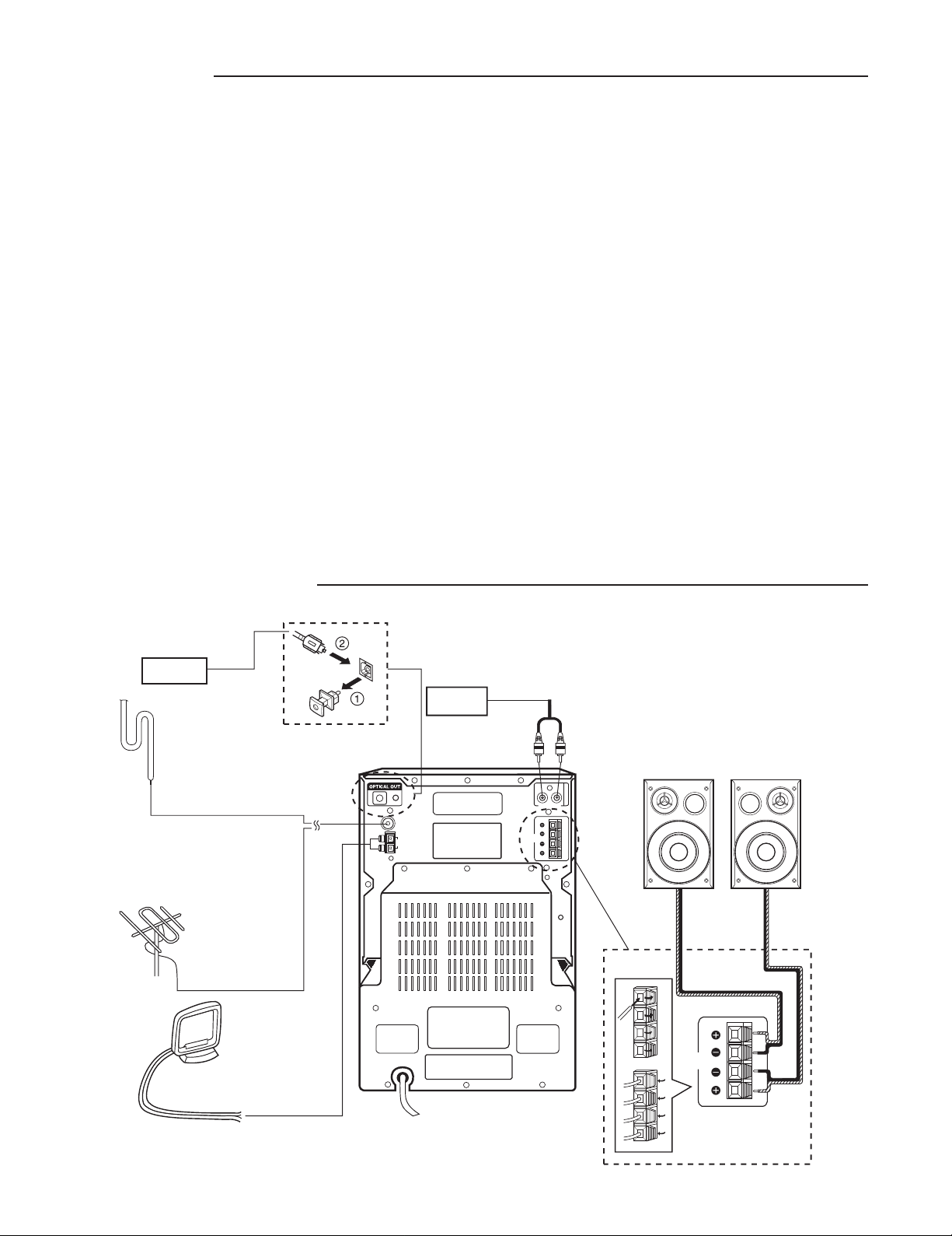
SYSTEM CONNECTIONS (XE)
Digital equipment
FM indoor aerial
FM outdoor aerial
Video equipment
FM
75
AM
LOOP
EXT.ANT
SPEAKERS
(6 MIN.)
R
VIDEO(AUDIO)
L
R
L ch speaker
L
IN
RESET
R ch speaker
AM loop aerial
To an AC outlet
- 1 -
SPEAKERS
(6
MIN.)
L
R
Page 3
SPEAKERS
(6
MIN.)
L
R
L
SPEAKERS
(6 MIN.)
VIDEO(AUDIO)
R
IN
RESET
L
R
FM 75
AM
LOOP
FM75
AM
LOOP
FM indoor aerial
FM
FM outdoor aerial
FM
AM loop aerial
AM
To an AC outlet
AC
Video equipment
L ch speaker
R ch speaker
✬
✲
✬
✳✰✥✡✫✥✲✳
✈✖ ✭✩✮✎✉
✶✩✤✥✯✈✡✵✤✩✯✉
✲
✩✮
✲✥✳✥✴
✦✭✗✕
✡✭
✬✯✯✰
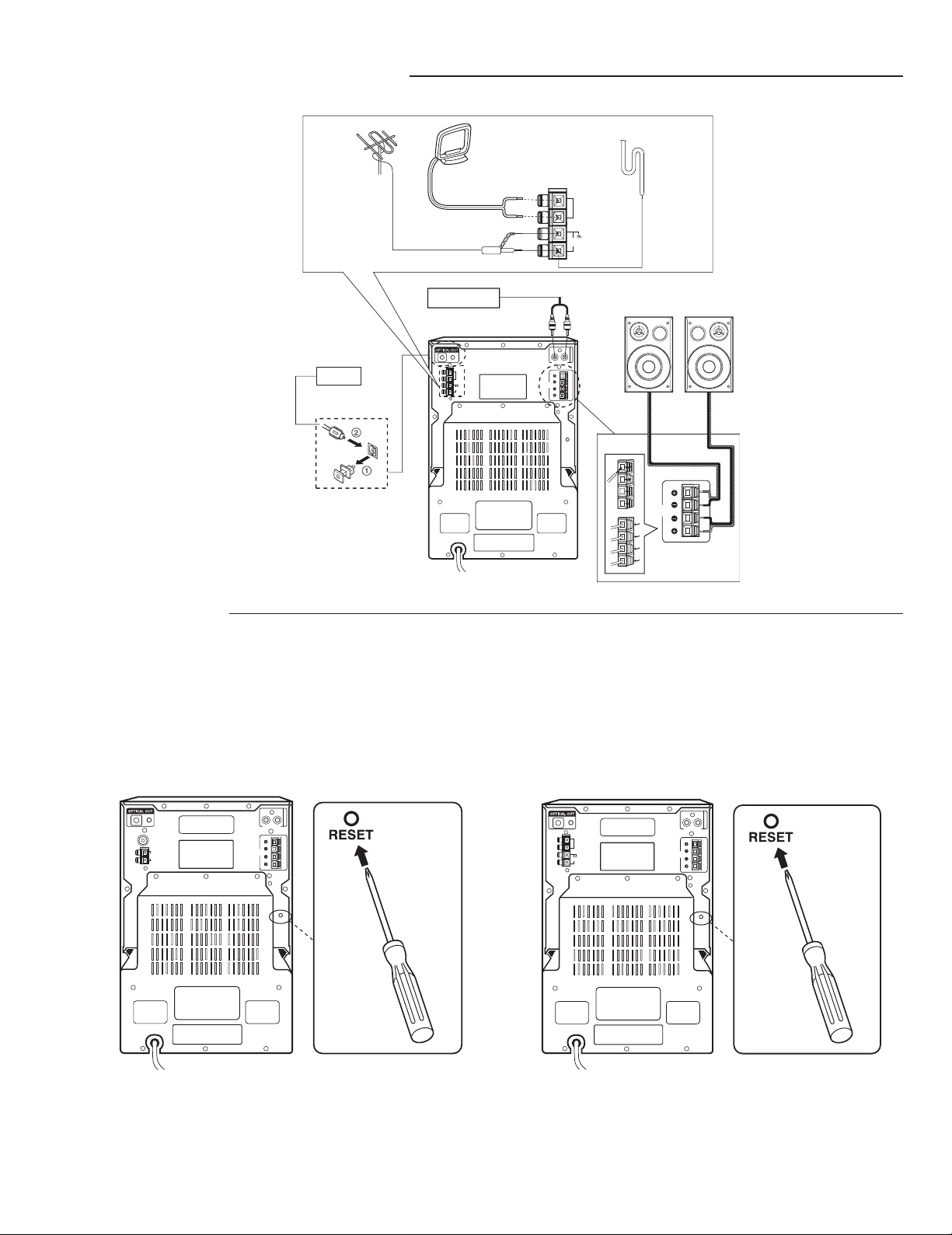
SYSTEM CONNECTIONS (KR & TW)
L
R
L
SPEAKERS
(6 MIN.)
VIDEO(AUDIO)
AM
LOOP
EXT.ANT
R
IN
FM
75
RESET
WHAT TO DO IF
If the operation of the unit or display is not normal, even though the appropriate buttons
have been pressed. Disconect the power cord from the AC outlet, then press "RESET"
(rear of the unit) for at least 30 seconds.
FOR XE FOR KR, TW
- 2 -
Page 4
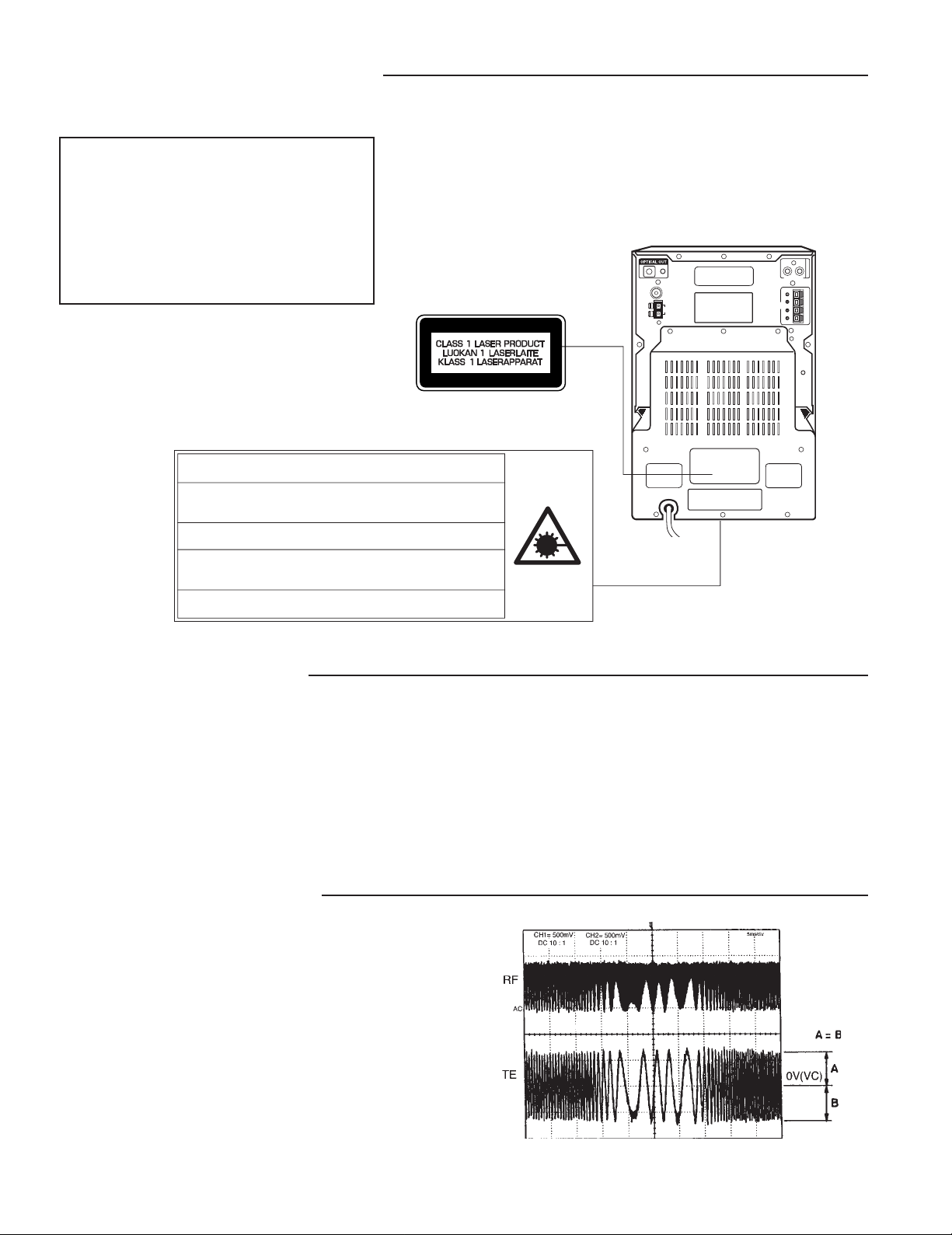
LASER BEAM SAFETY PRECAUTION
L
R
L
SPEAKERS
(6 MIN.)
VIDEO(AUDIO)
AM
LOOP
EXT.ANT
R
IN
FM
75
RESET
CAUTION INVISIBLE LASER RADIATION WHEN OPEN AND
INTERLOCKS DEFEATED. AVOID EXPOSURE TO BEAM.
ADVARSEL USYNLIG LASER STR LING VED BNING, N R
SIKKERHEDSAFBRYDERE ER UDE AF FUNKTION, UNDG UDS TTELSE
FOR STR LING.
VARNING OSYNLIG LASER STR LNING N R DENNA DEL R PPNAD
OCH SP RR R URKOPPLAD. STR LEN R FARLIG.
VORSICHT UNSICHTBARE LASERSTRAHLUNG TRITT AUS, WENN
DECKEL GE FFNET UND WENN SICHERHEITSVERRIEGELUNG
BERBR CKT IST. NICHT, DEM STRAHL AUSSETZEN.
VARO AVATTAESSA JA SUOJALUKITUS OHITETTAESSA OLET ALTTIINA
N KYM TT M LLE LASERS TEILYLLE. L KATSO S
TEESEEN.
• Pick-up that emits a laser beam is used in this CD player section.
(For XE Only)
CAUTION :
USE OF CONTROLS OR ADJUSTMENTS
OR PERFORMANCE OF PROCEDURES
OTHER THAN THOSE SPECIFIED HEREIN
MAY RESULT IN HAZARDOUS RADIATION
EXPOSURE
LASER OUTPUT..........0.6 mW Max. (CW)
WAVELENGTH .............790 nm
(For XE & KR)
(For XE Only)
CD PICK-UP MAINTENANCE
About pick-up (Optical lens) Cleaning
Clean a lens with swab of the cotton which moistened it with alcohol, cleaning paper or cleaning disc appointed.
Specified cleaning disc : LC-1 (Part code : 645 026 1961 ..... manufactured by SANYO.)
Show a clean procedure in the following in reference by swab of cotton.
1. Cotton swab is wrapped with Cleaning paper.
2. Add the isopropyl alcohol.
3. Gently move the tip of cotton swab just like a draw a whirlpool from inside to outside on the surface of lens.
CD PLAYER ADJUSTMENTS
1. ADJUSTMENTS
(1) Confirm the tracking balance
1. Turn on the POWER switch.
2. Connect an Oscilloscope to TP2 (TE) and TP4 (VC).
3. Set the test disc.
4. Press "PLAY" button to turn into the "PLAY" mode.
5. Keep holding "SKIP" button down so as to be "SERCH"
mode, then confirm that the oscilloscope waveform is
symmetrical on the top and bottom in relation to 0V (VC).
- 3 -
200mV/div.
5ms/div.
Page 5
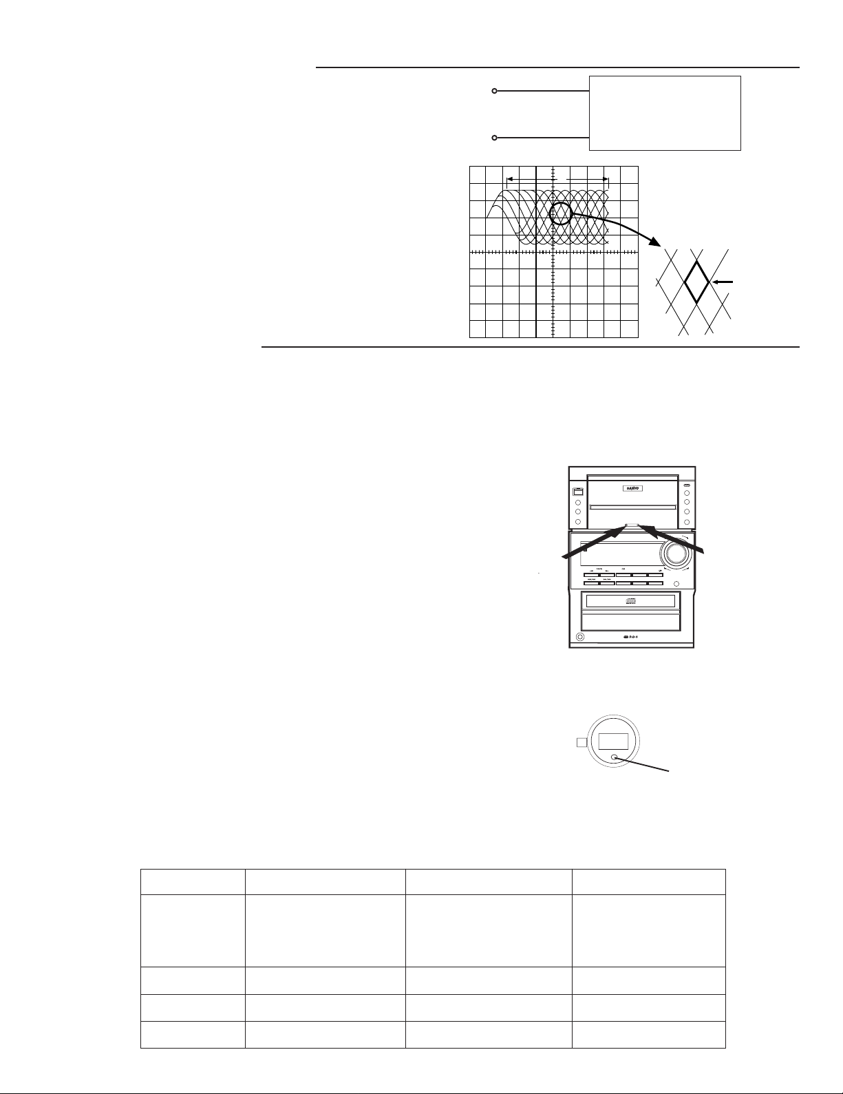
CD PLAYER ADJUSTMENTS
(2) Checking the "eye" pattern
1. Switch "ON" the POWER.
2. Connect an oscilloscope to TP1 (RF) and TP4 (VC).
3. Load the test disc.
4. Press the PLAY button.
5. Check to be sure that the "eye" pattern is at the center of
waveform and that the diamond shape is clearly defined.
6. Press the STOP button.
7. Turn off the POWER switch.
TAPE ADJUSTMENTS
1. Azimuth Adjustment
• Be sure to clean the heads before attempting to make any adjustment.
• Be sure both channels (1 and 2) are the same level.
(Using a dual-channel oscilloscope)
• Be sure both channel's waveform are same for the phase matching.
• After completion of the adjustment, use the threadlock (TB-1401B) to
secure the azimuth adjustment screws.
1. Remove the cover deck as Fig.1.
2. Load a test tape (VTT-738 etc. : 10kHz) in the Deck.
3. Press the PLAY button. (Normal playback)
4. Use a + tip screwdriver to turn the screw for normal azimuth
adjustment so that the left and right outputs are maximized at
the same phase during normal playback. See Fig.1.
5. Press the PLAY button. (Reverse playback)
6. Use a + tip screwdriver to turn the screw for reverse azimuth
adjustment so that the left and right outputs are maximized
at the same phase during reverse playback.
7. Adjust so that the waveforms for the left and right channels are in alignment.
TP1
(RF)
TP4
(VC)
NORMAL
+
OSCILLOSCOPE
-
a
OPENING EXPANDED
b
EJECT
SOUNDPRESET
CLOCK/TIME
TUNING
+
TUNING-
REVERSE
TUNER/BAND
VOLUME
+
PTYCHECK/
/
SYSTEM
REVERSE
PTYSELECT
OPEN/CLOSE
Fig.1
ST ANDBY
/ON
RDSMODE
MEMORY
FULLLOGIC CONTROL/AUTO
FUNCTION
MULTIFUNCTION DISPLAY
BASS
XPANDER
PRESET PRESET+
MICRO COMPONENT
PHONES
2. Tape Speed Adjustment
Fig.2
• Connect the Frequency Counter to TAPE OUT.
1. Insert the test tape (MTT-111N, etc.; 3,000Hz) into the DECK.
MOTOR
2. Press the PLAY button. .
3. Adjust a hole on the motor bottom so that a frequency counter reading of 3,000 ±5Hz is obtained.See Fig.2.
4. Press the STOP button, and eject the test tape.
3. Torque Measurement
Pull tentionItem
Driving power cassette :
TW-2412 (PLAY)
TW-2422(REV. PLAY)
-
-
Test Cassette
PLAY/REV.
F.FWD
REW
Take-up Torque Back tention
PLAY : TW2111A (FWD)
PLAY : TW2121A (REV)
F.FWD / REW : TW2231
30 ~ 65 grcm
70 ~ 140 grcm
70 ~ 140 grcm
PLAY : TW2111A (FWD)
PLAY : TW2121A (REV)
2 ~ 6 grcm
-
-
- 4 -
hole for adjustment
>50grcm
Page 6
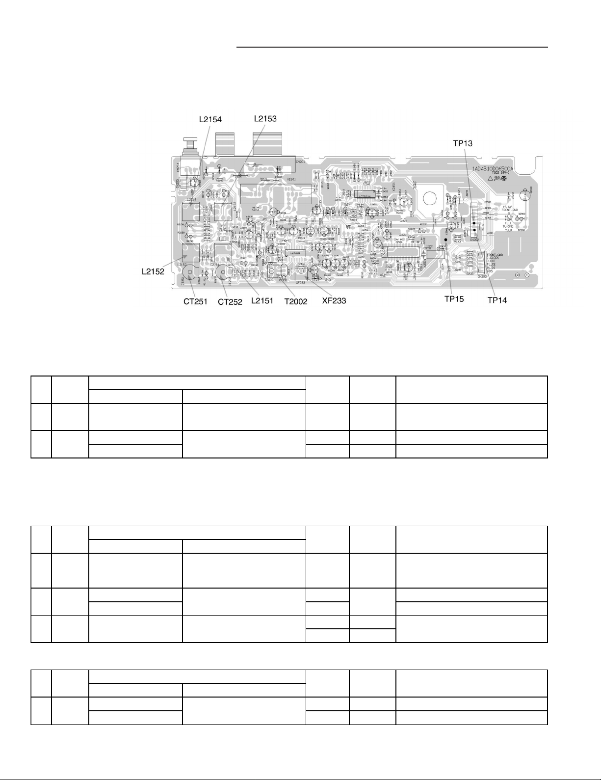
TUNER ADJUSTMENTS (XE ONLY)
• Use a plastic screw driver for adjustments.
• MODE : ST (Stereo)
• Speaker impedance : 6 ohm
• TUNING
FM : 87.5 - 108MHz, 50KHz
MW: 522 - 1611 kHz, 9 kHz step
520 - 1611 kHz, 9 kHz step
LW: 144 - 288 kHz, 9 kHz step
Antenna : 75 unbalanced , Modulation : 1 kHz
Dev. : ±22.5kHz (MONO), 22.5kHz (STEREO) ±6.75kHz (PILOT)
RF LeveL : dBuV EMF
1. FM
Step Adjusting Connection SG Adjustment Remark
Circuit Input Output Frequency
IF(0V)
1
Adjustme
nt
2 Cover --- Connect Digital DC voltmeter to 87.5MHZ --- 1.35±0.10V check only
Voltage --- TP11(H), TP12(E). 108.0MHZ --- 6.5±0.50V check only
FM Antenna SG=66dB µV
Alignment voltage IC231 Alignment voltage IC231
3-22pin(TP24,25) is 0.00±0.05V 3-22pin is 0.00 ±0.05V
Output Level : about 500mW at TP13, TP14, TP15
98MHz
XF233
SG Modulation : 1kHz, 30%
Antenna : IRE Loop
RF Level : dBuV EMF
2. MW
Step Adjusting Connection SG Adjustment Remark
Circuit Input Output Frequency
1
IF
Adjustme
nt
2 Cover --- Connect Digital DC voltmeter to 522kHZ 1.00±0.05V
Voltage --- TP11(H )and TP12(E). 1611kHZ 7.30±0.50V check only
3 Tracking Connect to VTVM 603KHZ L2151
LOOP ANT
Connect Sweep generator to test
point TP13(L)or TP14(R) and TP15(E)
point TP13(L)or TP14(R) and TP15(E)
3. LW
Step Adjusting Connection SG Adjustment Remark
Circuit Input Output Frequency
1 Cover --- Connect Digital DC voltmeter to 144kHZ L2154 1.00±0.05V
Voltage --- TP11(H) and TP12(E). 288kHZ --- 5.80±0.30V check only
Output Level : about 500mW at TP13, TP14, TP15
at 999kHz
1404kHZ CT252
T2002 AF MaximumLOOP ANT
L2153
AF Maximum
- 5 -
Page 7
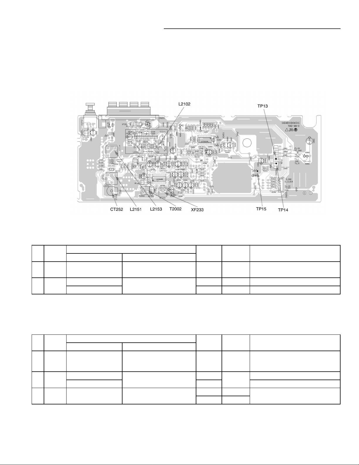
TUNER ADJUSTMENTS (For KR & TW)
• Use a plastic screw driver for adjustments.
• MODE : ST (Stereo)
• Speaker impedance : 6 ohm
• TUNING
FM : 87.5 - 108MHz, 50KHz step
AM: 522 - 1710kHz (TW)
522 - 1710KHz (9KHz step) (KR)
520 - 1710KHz (10KHz step) (KR)
Antenna : 75 unbalanced , Modulation : 1 kHz
Dev. : ±22.5kHz(MONO) 22.5kHz(STEREO) ±6.75kHz(PILOT)
RF LeveL : dBuV EMF
1. FM
Step Adjusting Connection SG Adjustment Remark
Circuit Input Output Frequency
IF(0V)
1
Adjustme
nt
2 Cover --- Connect Digital DC voltmeter to 87.5MHZ --- 1.00±0.05V check only
Voltage --- TP11(H), TP12(E). 108.0MHZ --- 6.5±0.50V check only
FM Antenna SG=66dB µV
Alignment voltage IC231 Alignment voltage IC231
3-22pin(TP24,25) is 0.0±0.05V 3-22pin is 0.0±0.05V
Output Level : about 500mW at TP13, TP14, TP15
98MHz
XF233
SG Modulation : 1kHz, 30%
Antenna : IRE Loop
RF Level : dBuV EMF
2. AW
Step Adjusting Connection SG Adjustment Remark
Circuit Input Output Frequency
1
IF
Adjustme
nt
2 Cover --- Connect Digital DC voltmeter to 522kHZ 1.00±0.05V check only
Voltage --- TP11(H )and TP12(E). 1611kHZ 8.1±0.50V check only
3 Tracking Connect to VTVM 603KHZ L2151
LOOP ANT
Connect Sweep generator to test
point TP13(L)or TP14(R) and TP15(E)
point TP13(L)or TP14(R) and TP15(E)
Output Level : about 500mW at TP13, TP14, TP15
at 999kHz
1404kHZ CT252
T2002 AF MaximumLOOP ANT
L2153
AF Maximum
- 6 -
Page 8
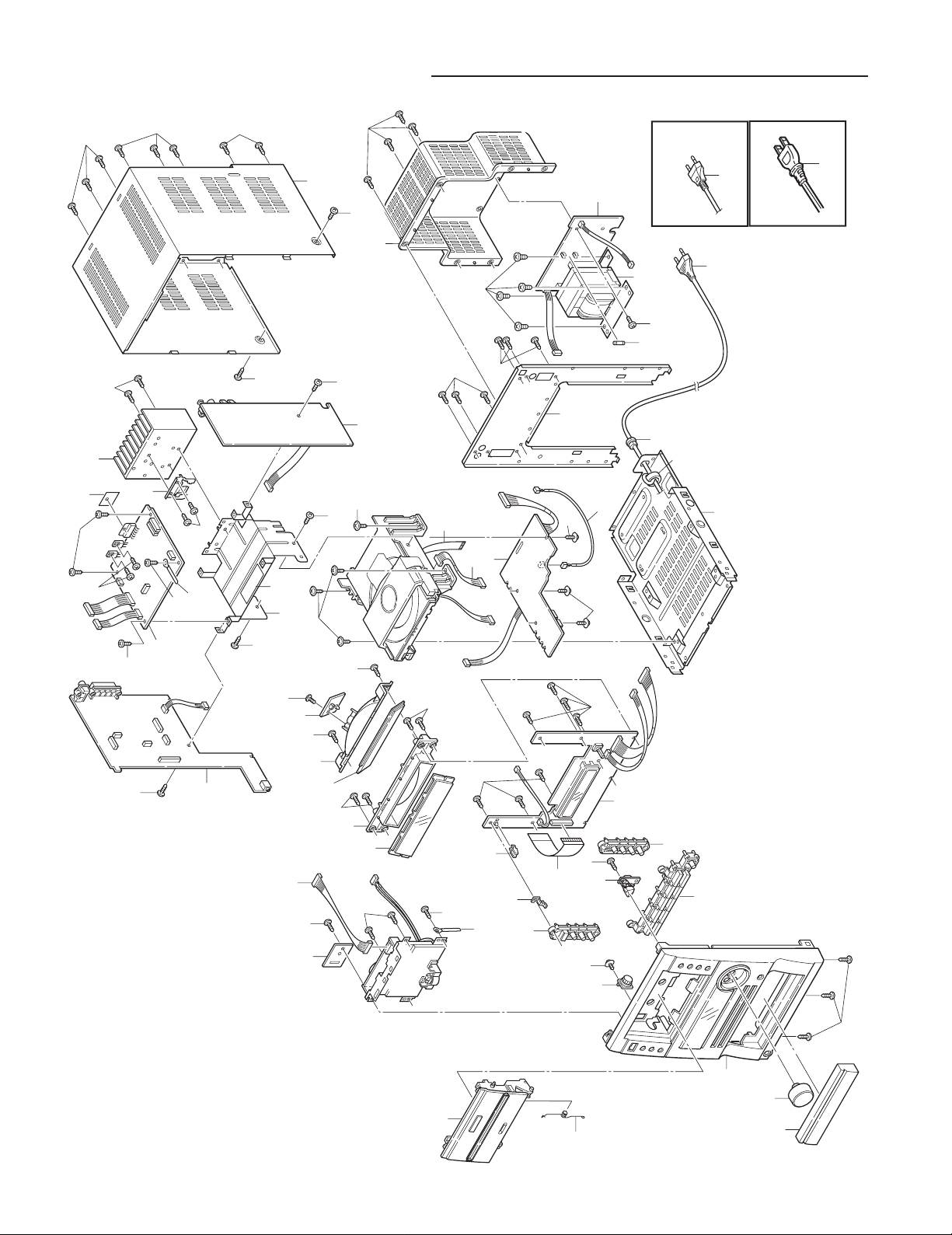
EXPLODED VIEW (CABINET & CHASSIS)
(NSP)
1
5
4
2
6
Y02
Y03
Y01
Y04
Y05
Y05
Y05
Y06
Y06
Y07
Y07
Y08
Y09
Y10
Y10
Y11
Y12
Y13
Y14
Y14
Y15
Y16
Y18
Y18
Y17
Y17
Y19
Y21
Y22
Y22
Y22
Y22
Y22
Y20
Y16
Y10
Y04
8
12
52
13
72
73
74
75
76
55
56
57
59
58(XE)
60
77
14
16
17
18
15
7
9
3
10
11
71
51
19
20
21
22
23
53
54
24
Y12
61
Y23
(KR)
(TW)
58
58
N.S.P : Not supplied as service parts.
- 7 -
Page 9

PARTS LIST
PRODUCT SAFETY NOTICE
EACH PRECAUTION IN THIS MANUAL SHOULD BE FOLLOWED DURING SERVICING. COMPONENTS IDENTIFIED WITH THE IEC
SYMBOL IN THE PARTS LIST AND THE SCHEMATIC DIAGRAM DESIGNATED COMPONENTS IN WHICH SAFETY CAN BE OF
SPECIAL SIGNIFICANCE. WHEN REPLACING A COMPONENT IDENTIFIED BY , USE ONLY THE REPLACEMENT PARTS DESIGNATED,
OR PARTS WITH THE SAME RATINGS OF RESISTANCE, WATTAGE OR VOLTAGE THAT ARE DESIGNATED IN THE PARTS LIST
IN THIS MANUAL. LEAKAGE-CURRENT OR RESISTANCE MEASUREMENTS MUST BE MADE TO DETERMINE THAT EXPOSED
PARTS ARE ACCEPTABLY INSULATED FROM THE SUPPLY CIRCUIT BEFORE RETURNING THE PRODUCT TO THE CUSTOMER.
CAUTION : Regular type resistors and capacitors are not listed. To know those values, refer to the schematic diagram.
Regular type resistors are less than 1/4 W Carbon type and Chip type resistors.
Regular type capacitors are less than 50 V and less than 1000 µF type of Ceramic type, Electrolytic type and Chip type.
: Not supplied as service parts.
N.S.P
PACKING & ACCESSORIES
REF.NO. PART NO. DESCRIPTION
614 318 6380 CARTON CASE (XE)
614 319 6297 CARTON CASE (KR)
614 320 5944 CARTON CASE (TW)
614 318 6397 CUSHION,RIGHT
614 318 6403 CUSHION,LEFT
614 318 6410 INSTRUCTION MANUAL (XE)
614 318 6427 INSTRUCTION MANUAL,GREECE (XE)
614 319 5092 INSTRUCTION MANUAL (KR)
614 320 5951 INSTRUCTION MANUAL (TW)
645 012 1326 POLY SHEET-1200X0550*NC,SET (XE)
645 012 1302 POLY SHEET-1200X0550*NC,
SET (KR, TW)
645 044 1110 REMOCON,***
645 046 8322 ASSY,ANTENA,LOOP
or 645 005 1227 ASSY,ANTENA,LOOP
614 308 5515 ANTENNA (XE)
or 614 229 4635 ANTENNA (XE)
614 245 0055 ANTENNA (KR, TW)
614 318 9404 LID,BATTERY,SERVICE
614 318 5789 ASSY,BOX,SPEAKER (L) (XE)
614 319 4934 ASSY,BOX,SPEAKER (L) (KR, TW)
614 318 5796 ASSY,BOX,SPEAKER (R) (XE)
614 319 4941 ASSY,BOX,SPEAKER (R) (KR, TW)
614 318 5819 ASSY,GRILLE (XE)
614 319 4965 ASSY,GRILLE (KR, TW)
CABINET & CHASSIS
REF.NO. PART NO. DESCRIPTION
1 614 318 6007 COVER,CD,DOOR
2 614 318 7066 KNOB,VOLUME
3 614 318 5895 ASSY,PANEL,FRONT (XE)
3 614 319 5009 ASSY,PANEL,FRONT (KR, TW)
4 614 318 5888 ASSY,LID,CASSETTE
5 614 318 6267 SPRING,LID,CASSETTE
6 614 309 8270 ASSY,GEAR,LID CASSETTE
7 614 318 5932 BUTTON,POWER,4KEYS
8 614 318 7530 REFLECTOR,STANDBY,LED
9 614 303 1277 LATCH,CAM,DECK,DOOR.LOCKING
10 614 318 5956 BUTTON,PLAY,11KEYS
11 614 318 5949 BUTTON,TUNER,4KEYS
12 614 318 7486 HOLDER,STANDBY LED
13 614 318 6052 DEC,WINDOW,LED
14 614 318 6090 HOLDER,LED
15 614 318 6236 REFLECTOR
16 614 318 6106 HOLDER,REFLECTOR
17 614 318 6083 HOLDER,HEAT SINK
18 614 312 0223 MOUNTING,POWER IC
19 614 318 7424 ASSY,CABINET,BOTTOM
20 614 284 1884 FIXER,AC CORD
or 614 129 1901 FIXER,AC CORD
21 614 318 7103 PANEL,REAR (XE)
21 614 319 5030 PANEL,REAR (KR)
REF.NO. PART NO. DESCRIPTION
21 614 320 5869 PANEL,REAR (TW)
22 614 318 6885 COVER,REAR (XE, TW)
22 614 319 4477 COVER,REAR (KR)
23 614 322 8042 ASSY,CABINET,BENDING
24 614 317 3090 LABEL,SAFETY,LASER,PICK-UP
FIXING PARTS
REF.NO. PART NO. DESCRIPTION
Y01 411 021 3503 SCR S-TPG BIN 3X10,
P-FRONT+C-BOTTOM
Y02 411 021 3503 SCR S-TPG BIN 3X10,
F-PANEL+ASSY,GEAR
Y03 411 021 3503 SCR S-TPG BIN 3X10,
F-PANEL+LATCH,CAM
Y04 411 021 3503 SCR S-TPG BIN 3X10,FRONT+PCB
Y05 411 021 3503 SCR S-TPG BIN 3X10,
F-PANEL+MECHA
Y06 411 021 3503 SCR S-TPG BIN 3X10,
HOLDER,LED+F-PANEL
Y07 411 021 3503 SCR S-TPG BIN 3X10,
H-REFLECTOR+H-LED
Y08 411 021 3503 SCR S-TPG BIN 3X10,
H-REFLECTOR+PWB
Y09 411 021 3503 SCR S-TPG BIN 3X10,
PRE AMP PWB+HOLDER
Y10 411 021 3503 SCR S-TPG BIN 3X10,
AMP,PWB+HOLDER
Y11 614 129 9136 LUG
Y12 411 021 3503 SCR S-TPG BIN 3X10,HEAT SINK
Y13 411 021 3503 SCR S-TPG BIN 3X10,
HOLDER+HEAT,SINK
Y14 411 021 3503 SCR S-TPG BIN 3X10,
HOLDER+CD,MECHA
Y15 411 021 3503 SCR S-TPG BIN 3X10,
TUNER,PWB+HOLDER
Y16 411 020 8905 SCR S-TPG BRZ+FLG 3X10,
CD MECHA + C-BOTTOM
Y17 411 020 9902 SCR S-TPG BRZ+FLG 3X8,
CD MECHA + CD PWB
Y18 411 021 3701 SCR S-TPG BIN 3X10,
P-REAR+ELECT PARTS
Y19 411 001 3905 SCR S-TPG BIN 4X6,
P-TRANS + C-BOTTOM
Y20 411 021 3503 SCR S-TPG BIN 3X10,
C-REAR + POWER PWB
Y21 411 021 3701 SCR S-TPG BIN 3X10,
COVER,REAR+P-REAR,
C-REAR+C-BOTTOM
Y22 411 021 3701 SCR S-TPG BIN 3X10,
P-REAR+CABINET,TOP,
C-TOP+C-BOTTOM
Y23 614 129 9082 LUG,TAPE MECHA (XE)
- 8 -
Page 10

PARTS LIST
ELECTRICAL PARTS
REF.NO. PART NO. DESCRIPTION
51 645 050 3788 FLEXIBLE FLAT CABLE,
FRONT TO AMP
52 614 320 3292 ASSY,WIRE,AMP TO DECK MOTOR
53 614 310 8887 SPACER,RUBBER,POWER IC
54 614 318 9374 HEAT SINK
55 614 320 3360 ASSY,WIRE,CD BASE MECHA
56 614 320 3407 ASSY,WIRE,TUNER TO CD(OPT.)
57 645 031 7637 CORE,FERRITE,EMC
or 645 051 0649 CORE,FERRITE,EMC
58 645 016 9939 CORD,POWER-1.74MK (XE)
58 645 047 8055 CORD,POWER-1.8MK (KR)
58 645 044 6474 CORD,POWER-1.7MK (TW)
59 423 017 0007 FUSE 250V 1A (XE,KR)
59 423 021 6804 FUSE 125V 2A (TW)
60 645 048 6012 TRANS,POWER (XE)
60 645 050 2071 TRANS,POWER (KR)
60 645 050 8905 TRANS,POWER (TW)
61 614 320 3315 ASSY,WIRE,AMP TO R/P HEAD
62 645 050 3795 FLEXIBLE FLAT CABLE,CD,PICK UP
63 614 320 3346 ASSY,WIRE,PT TO AMP FL (XE, KR)
FRONT P.W.BOARD ASSY
REF.NO. PART NO. DESCRIPTION
71 614 318 5130 ASSY,PWB,FRONT(Only initial)(XE)
71 614 319 1605 ASSY,PWB,FRONT(Only initial)(KR)
71 614 320 8259 ASSY,PWB,FRONT(Only initial)(TW)
BR601 614 318 6991 HOLDER,FL,HOLDER-FL
CN601 645 012 5324 SOCKET,FPC 28P,FRONT-AMP
CN604 614 035 4911 SOCKET,DIP 2P,FRONT-LED
CN612 614 320 3414 ASSY,WIRE,FRONT-POWER AMP 12P
CN613 614 320 3438 ASSY,WIRE,FRONT-TU
CN614 614 320 3285 ASSY,WIRE,FRONT-CD TRAY LED 2P
D6010 407 012 4406 DIODE 1SS133
D6110 407 012 4406 DIODE 1SS133
D6312 408 032 5404 LED SLP-9118C-51H-S-T1,
STAND-BY-LED
DE601 408 039 8507 PHOTO DIODE PIC-28043TE3
FL601 645 048 3165 FLOURESCENT TUBE,FL
IC601 410 423 5306 IC LC866540A-5Y58 (XE, KR)
IC601 410 427 9102 IC LC866540A-5Y89 (TW)
L6010 645 001 5441 INDUCTOR,2.2U K
Q6108 405 143 8706 TR KTC3199-GR
or 405 011 8500 TR 2SC1740S-R
or 405 011 8609 TR 2SC1740S-S
or 405 017 9600 TR 2SC3330-T
or 405 017 9709 TR 2SC3330-U
Q6201 405 000 6104 TR DTC144ES
or 405 146 1209 TR KRC104M
Q6202 405 000 6104 TR DTC144ES
or 405 146 1209 TR KRC104M
Q6301 405 143 0007 TR KRC107M
or 405 000 3806 TR DTC114YS
SE601 407 217 1101 PHOTO DIODE, SPS-442-1G (KR)
S6001 645 044 6535 SWITCH,ROTARY(ENCODER)
S6110 645 006 5958 SWITCH,PUSH 1P-1T
or 614 220 5471 SWITCH,TACT
or 614 240 1002 SWITCH,TACT
S6111 645 006 5958 SWITCH,PUSH 1P-1T
or 614 240 1002 SWITCH,TACT
or 614 220 5471 SWITCH,TACT
S6112 645 006 5958 SWITCH,PUSH 1P-1T
or 614 240 1002 SWITCH,TACT
or 614 220 5471 SWITCH,TACT
S6113 614 220 5471 SWITCH,TACT
or 614 240 1002 SWITCH,TACT
or 645 006 5958 SWITCH,PUSH 1P-1T
REF.NO. PART NO. DESCRIPTION
S6114 614 220 5471 SWITCH,TACT
or 614 240 1002 SWITCH,TACT
or 645 006 5958 SWITCH,PUSH 1P-1T
S6115 614 220 5471 SWITCH,TACT
or 614 240 1002 SWITCH,TACT
or 645 006 5958 SWITCH,PUSH 1P-1T
S6116 614 220 5471 SWITCH,TACT
or 614 240 1002 SWITCH,TACT
or 645 006 5958 SWITCH,PUSH 1P-1T
S6117 614 240 1002 SWITCH,TACT
or 645 006 5958 SWITCH,PUSH 1P-1T
or 614 220 5471 SWITCH,TACT
S6118 614 220 5471 SWITCH,TACT
or 614 240 1002 SWITCH,TACT
or 645 006 5958 SWITCH,PUSH 1P-1T
S6119 614 220 5471 SWITCH,TACT
or 614 240 1002 SWITCH,TACT
or 645 006 5958 SWITCH,PUSH 1P-1T
S6210 614 220 5471 SWITCH,TACT
or 614 240 1002 SWITCH,TACT
or 645 006 5958 SWITCH,PUSH 1P-1T
S6211 614 220 5471 SWITCH,TACT
or 614 240 1002 SWITCH,TACT
or 645 006 5958 SWITCH,PUSH 1P-1T
S6212 614 220 5471 SWITCH,TACT
or 614 240 1002 SWITCH,TACT
or 645 006 5958 SWITCH,PUSH 1P-1T
S6213 645 006 5958 SWITCH,PUSH 1P-1T
or 614 240 1002 SWITCH,TACT
or 614 220 5471 SWITCH,TACT
S6214 614 220 5471 SWITCH,TACT
or 614 240 1002 SWITCH,TACT
or 645 006 5958 SWITCH,PUSH 1P-1T
S6215 614 220 5471 SWITCH,TACT
or 614 240 1002 SWITCH,TACT
or 645 006 5958 SWITCH,PUSH 1P-1T
S6216 614 220 5471 SWITCH,TACT
or 614 240 1002 SWITCH,TACT
or 645 006 5958 SWITCH,PUSH 1P-1T
S6217 614 220 5471 SWITCH,TACT
or 614 240 1002 SWITCH,TACT
or 645 006 5958 SWITCH,PUSH 1P-1T
S6218 614 220 5471 SWITCH,TACT
or 614 240 1002 SWITCH,TACT
or 645 006 5958 SWITCH,PUSH 1P-1T
X6101 645 032 1627 OSC,CRYSTAL 32.768KHZ
X6102 645 018 6103 OSC,CERAMIC 6.000MHZ
CD TRAY LED P.W.BOARD ASSY
REF.NO. PART NO. DESCRIPTION
72 614 318 5123 ASSY,PWB,CD TRAY LED(Only initial)
CN645 614 310 2434 PLUG,2P
or 645 005 7366 PLUG,2P
D6401 407 225 4507 LED LT03B3-41-URE1,
CD TRAY LIGHT
- 9 -
Page 11

PARTS LIST
PRE AMPLIFIER P.W.BOARD ASSY
REF.NO. PART NO. DESCRIPTION
73 614 318 5109 ASSY,PWB,PRE AMP(Only Initial) (XE)
73 614 319 1490 ASSY,PWB,PRE AMP(Only Initial)
(KR, TW)
C4720 403 059 3204 POLYESTER 2200P J 50V
C4721 403 061 7702 POLYESTER 4700P J 50V
C4722 403 061 3605 POLYESTER 0.039U J 50V
C4730 403 060 2807 POLYESTER 0.027U K 50V
C4741 403 057 3503 POLYESTER 0.1U K 50V
C4861 403 304 4802 DL-ELECT 0.047F Z 5.5V
or 403 262 8607 DL-ELECT 0.047F Z 5.5V
C4982 403 057 1202 POLYESTER 0.01U M 50V
C4992 403 057 1202 POLYESTER 0.01U M 50V
CN413 614 320 3308 ASSY,WIRE,POWERAMP-PREAMP 4P
CN450 645 006 0861 PLUG,7P
or 614 310 2489 PLUG,7P
CN451 645 005 8165 PLUG,11P
or 614 310 2526 PLUG,11P
CN452 614 020 1239 SOCKET,4P
CN460 645 012 5324 SOCKET,FPC 28P,SOCKET FPC28P
CN470 645 005 8158 PLUG,10P
or 614 310 2519 PLUG,10P
CN471 645 005 8127 PLUG,6P
or 614 310 2472 PLUG,6P
CN480 645 005 9292 PLUG,5P
or 614 310 2465 PLUG,5P
CN481 645 011 6384 JACK,PHONE D3.6,HEAD PHONE
CN485 614 276 6835 SOCKET,JACK
CN490 645 008 5314 TERMINAL,SPEAKER-OUT
D4840 407 099 4603 ZENER DIODE MTZJ3.9B
D4850 407 012 4406 DIODE 1SS133
D4851 407 012 4406 DIODE 1SS133
D4950 407 012 4406 DIODE 1SS133
D4960 407 099 5204 ZENER DIODE MTZJ5.1B
IC450 409 474 6103 IC LC75342M
IC460 409 451 7406 IC AN7348K
IC470 409 189 3404 IC BA7755A
L4700 645 037 2858 CORE,PIPE
L4720 645 006 1523 INDUCTOR,470U J
L4721 645 037 2858 CORE,PIPE
L4740 645 006 1523 INDUCTOR,470U J
L4741 645 006 1523 INDUCTOR,470U J
L4810 645 006 9864 INDUCTOR,80U (XE)
L4820 645 006 9864 INDUCTOR,80U (XE)
L4910 645 006 9864 INDUCTOR,80U (XE)
L4920 645 006 9864 INDUCTOR,80U (XE)
PR496
Q4610 405 143 0007 TR KRC107M
or 405 000 3806 TR DTC114YS
Q4620 405 000 3806 TR DTC114YS
or 405 143 0007 TR KRC107M
Q4700 405 155 0002 TR MPSA56
Q4701 405 000 3806 TR DTC114YS
or 405 143 0007 TR KRC107M
Q4720 405 141 3307 TR KTC3198-GR
or 405 019 3804 TR 2SC536-G-NP
or 405 019 2708 TR 2SC536-F-NP
or 405 141 3208 TR KTC3198-Y
Q4730 405 019 3804 TR 2SC536-G-NP
or 405 019 2708 TR 2SC536-F-NP
or 405 141 3208 TR KTC3198-Y
or 405 141 3307 TR KTC3198-GR
Q4840 405 004 5004 TR 2SA608-G-NP
or 405 004 4502 TR 2SA608-F-NP
or 405 141 3505 TR KTA1266-Y
or 405 141 3406 TR KTA1266-GR
Q4850 405 019 3804 TR 2SC536-G-NP
or 405 019 2708 TR 2SC536-F-NP
or 405 141 3208 TR KTC3198-Y
645 014 2475 PROTECTOR,0.75A 125V
REF.NO. PART NO. DESCRIPTION
or 405 141 3307 TR KTC3198-GR
Q4930 405 155 0002 TR MPSA56
Q4931 405 143 0007 TR KRC107M
or 405 000 3806 TR DTC114YS
Q4940 405 155 0002 TR MPSA56
Q4941 405 000 3806 TR DTC114YS
or 405 143 0007 TR KRC107M
Q4970 405 004 5004 TR 2SA608-G-NP
or 405 004 4502 TR 2SA608-F-NP
or 405 141 3505 TR KTA1266-Y
or 405 141 3406 TR KTA1266-GR
S4900 614 215 9828 SWITCH,TACT
POWER AMPLIFIER P.W.BOARD ASSY
REF.NO. PART NO. DESCRIPTION
74 614 318 5093 ASSY,PWB,POWER AMP(Only Initial)
(XE)
74 614 319 1483 ASSY,PWB,POWER AMP(Only Initial)
(KR, TW)
C4100 403 329 6201 ELECT 2200U M 35V
or 403 325 0203 ELECT 2200U M 35V
C4120 403 329 6102 ELECT 1000U M 35V (XE)
C4200 403 329 6102 ELECT 1000U M 35V (XE)
C4432 403 059 8209 POLYESTER 0.22U K 50V
C4433 403 059 8209 POLYESTER 0.22U K 50V
C4442 403 059 8209 POLYESTER 0.22U K 50V
C4443 403 059 8209 POLYESTER 0.22U K 50V
CN410 645 004 2911 PLUG,5P
or 614 310 2762 PLUG,5P
CN414 614 320 3384 ASSY,WIRE,PREAMP-POWERAMP 7P
CN415 614 320 3391 ASSY,WIRE,PREAMP-POWERAMP 11P
CN420 614 310 2441 PLUG,3P (XE)
or 645 005 7373 PLUG,3P (XE)
CN430 614 310 2496 PLUG,8P
or 645 005 8134 PLUG,8P
CN440 645 012 2729 SOCKET,DIP 7P
CN441 614 035 5000 SOCKET,DIP 11P
CN442 645 006 1813 PLUG,4P
CN443 645 006 0878 PLUG,12P (XE)
CN443 645 310 2533 PLUG,12P (KR)
CN444 645 006 0878 PLUG,12P (XE)
CN444 645 310 2533 PLUG,12P (KR)
D4110 407 196 5800 DIODE 1N5402BD82
D4111 407 196 5800 DIODE 1N5402BD82
D4112 407 196 5800 DIODE 1N5402BD82
D4113 407 196 5800 DIODE 1N5402BD82
D4210 407 099 6805 ZENER DIODE MTZJ13B
D4220 407 099 6102 ZENER DIODE MTZJ10B
D4300 407 148 6701 DIODE 1A3-I
D4301 407 148 6701 DIODE 1A3-I
D4310 407 099 5402 ZENER DIODE MTZJ6.2B
D4320 407 099 4603 ZENER DIODE MTZJ3.9B
D4321 407 012 4406 DIODE 1SS133
D4340 407 099 9509 ZENER DIODE MTZJ30B
D4341 407 012 4406 DIODE 1SS133
D4342 407 012 4406 DIODE 1SS133
D4343 407 012 4406 DIODE 1SS133
D4344 407 012 4406 DIODE 1SS133
HS431 614 215 9347 HEAT SINK,Q4310
IC440 409 441 6402 IC TDA7265
PR410 645 025 5137 PROTECTOR,7A 125V
PR411 645 025 5137 PROTECTOR,7A 125V
PR431 645 027 4169 PROTECTOR,0.125A 125V
PR434 645 014 2451 PROTECTOR,0.25A 125V
Q4210 405 019 3804 TR 2SC536-G-NP
or 405 019 2708 TR 2SC536-F-NP
or 405 141 3208 TR KTC3198-Y
or 405 141 3307 TR KTC3198-GR
- 10 -
Page 12

PARTS LIST
REF.NO. PART NO. DESCRIPTION REF.NO. PART NO. DESCRIPTION
Q4211 405 019 3804 TR 2SC536-G-NP
or 405 019 2708 TR 2SC536-F-NP
or 405 141 3208 TR KTC3198-Y
or 405 141 3307 TR KTC3198-GR
Q4212 405 138 6403 TR KTD2058Y
Q4220 405 019 3804 TR 2SC536-G-NP
or 405 019 2708 TR 2SC536-F-NP
or 405 141 3208 TR KTC3198-Y
or 405 141 3307 TR KTC3198-GR
Q4221 405 019 3804 TR 2SC536-G-NP
or 405 019 2708 TR 2SC536-F-NP
or 405 141 3208 TR KTC3198-Y
or 405 141 3307 TR KTC3198-GR
Q4222 405 138 6403 TR KTD2058Y
Q4310 405 138 6403 TR KTD2058Y
Q4320 405 004 5004 TR 2SA608-G-NP
or 405 004 4502 TR 2SA608-F-NP
or 405 141 3505 TR KTA1266-Y
or 405 141 3406 TR KTA1266-GR
Q4321 405 004 5004 TR 2SA608-G-NP
or 405 004 4502 TR 2SA608-F-NP
or 405 141 3505 TR KTA1266-Y
or 405 141 3406 TR KTA1266-GR
Q4330 405 141 3307 TR KTC3198-GR
or 405 141 3208 TR KTC3198-Y
or 405 019 2708 TR 2SC536-F-NP
or 405 019 3804 TR 2SC536-G-NP
Q4340 405 141 3604 TR KTA1273-Y
or 405 009 5207 TR 2SB927-S
or 405 009 5306 TR 2SB927-T
Q4400 405 141 3307 TR KTC3198-GR
or 405 141 3208 TR KTC3198-Y
or 405 019 2708 TR 2SC536-F-NP
or 405 019 3804 TR 2SC536-G-NP
Q4410 405 141 3307 TR KTC3198-GR
or 405 141 3208 TR KTC3198-Y
or 405 019 2708 TR 2SC536-F-NP
or 405 019 3804 TR 2SC536-G-NP
Q4420 405 141 3307 TR KTC3198-GR
or 405 019 3804 TR 2SC536-G-NP
or 405 019 2708 TR 2SC536-F-NP
or 405 141 3208 TR KTC3198-Y
R4120 402 083 3501 RESISTOR 1.5K J- 1W
R4211 402 081 2506 FUSIBLE RES 1 J- 1/2W
R4221 402 081 2506 FUSIBLE RES 1 J- 1/2W
R4300 402 082 1102 FUSIBLE RES 22 JA 1/2W
R4436 402 078 5107 FUSIBLE RES 4.7 JA 1/4W
or 402 081 2605 FUSIBLE RES 4.7 J- 1/4W
R4446 402 081 2605 FUSIBLE RES 4.7 J- 1/4W
or 402 078 5107 FUSIBLE RES 4.7 JA 1/4W
SA431 411 021 3503 SCR S-TPG BIN 3X10
TUNER P.W.BOARD ASSY (FOR XE)
REF.NO. PART NO. DESCRIPTION
75 614 318 5116 ASSY,PWB,TU (Only Initial)
C2457 403 259 0508 NP-ELECT 1U M 50V
CN201 645 032 6394 TERMINAL
or 614 255 5750 TERMINAL
CN202 645 012 2736 SOCKET,DIP 8P
CN203 645 005 8127 PLUG,6P
or 614 310 2472 PLUG,6P
CN204 407 215 1608 PHOTO COUPLE TOTX178A
or 407 218 1100 PHOTO COUPLE GP1FA550TZ
CN205 645 005 7373 PLUG,3P
or 614 310 2441 PLUG,3P
CN212 614 320 3339 ASSY,WIRE,TU-POWERAMP 8P
CT251 645 032 5236 TRIMMER,18PF
CT252 645 032 5663 TRIMMER,7PF
D2103 407 012 4406 DIODE 1SS133
D2104 407 012 4406 DIODE 1SS133
D2151 407 012 4406 DIODE 1SS133
D2153 407 105 1602 VARACTOR DI SVC342M-V
or 407 105 1305 VARACTOR DI SVC342L-V
D2301 407 063 9108 ZENER DIODE MTZJ6.8B
D2450 407 012 4406 DIODE 1SS133
D2451 407 012 4406 DIODE 1SS133
D2452 407 153 7502 ZENER DIODE GZS3.0B
D2453 407 012 4406 DIODE 1SS133
D2454 407 012 4406 DIODE 1SS133
D2455 407 012 4406 DIODE 1SS133
D2456 407 012 4406 DIODE 1SS133
D2466 407 012 4406 DIODE 1SS133
D2467 407 012 4406 DIODE 1SS133
IC231 409 474 3201 IC LA1844ML
IC241 409 439 4502 IC LC72121M-D
IC251 409 447 3900 IC LC72722
L2100 645 037 2858 CORE,PIPE
L2101 645 037 2858 CORE,PIPE
L2151 645 040 2685 TRANS,ANT,796KHZ
L2152 645 046 7998 TRANS,ANT,796KHZ
L2153 645 040 2708 TRANS,OSC,796KHZ
L2154 645 040 2722 TRANS,OSC,796KHZ
L2301 645 004 0580 INDUCTOR,1M J
L2451 645 001 4581 INDUCTOR,100U K
L2501 645 001 4581 INDUCTOR,100U K
L2502 645 001 4581 INDUCTOR,100U K
Q2140 405 020 7402 TR 2SC945A-P
or 405 020 7204 TR 2SC945A-K
or 405 019 3705 TR 2SC536-G-AUD-SPA
or 405 017 9709 TR 2SC3330-U
or 405 017 9600 TR 2SC3330-T
or 405 011 8609 TR 2SC1740S-S
or 405 011 8500 TR 2SC1740S-R
or 405 143 8706 TR KTC3199-GR
Q2152 405 016 0806 TR 2SC2839-E
or 405 151 4103 TR KTC3193-Y
or 405 151 4202 TR KTC3193-O
Q2153 405 016 0806 TR 2SC2839-E
or 405 151 4103 TR KTC3193-Y
or 405 151 4202 TR KTC3193-O
Q2154 405 151 4202 TR KTC3193-O
or 405 151 4103 TR KTC3193-Y
or 405 016 0806 TR 2SC2839-E
Q2155 405 016 0806 TR 2SC2839-E
or 405 151 4103 TR KTC3193-Y
or 405 151 4202 TR KTC3193-O
Q2156 405 016 0806 TR 2SC2839-E
or 405 151 4103 TR KTC3193-Y
or 405 151 4202 TR KTC3193-O
Q2157 405 035 8609 TR 2SK544-F
or 405 035 8708 TR 2SK544-E
Q2201 405 016 0806 TR 2SC2839-E
or 405 151 4103 TR KTC3193-Y
or 405 151 4202 TR KTC3193-O
Q2310 405 017 9600 TR 2SC3330-T
or 405 011 8609 TR 2SC1740S-S
or 405 011 8500 TR 2SC1740S-R
or 405 143 8706 TR KTC3199-GR
or 405 017 9709 TR 2SC3330-U
or 405 019 3705 TR 2SC536-G-AUD-SPA
or 405 020 7402 TR 2SC945A-P
or 405 020 7204 TR 2SC945A-K
Q2451 405 036 3702 TR 2SA1564
or 405 151 5209 TR KRA107M
or 405 000 0904 TR DTA114YS
or 405 078 2404 TR BN1A4P
- 11 -
Page 13

PARTS LIST
REF.NO. PART NO. DESCRIPTION
Q2452 405 036 3702 TR 2SA1564
or 405 151 5209 TR KRA107M
or 405 000 0904 TR DTA114YS
or 405 078 2404 TR BN1A4P
Q2453 405 036 3702 TR 2SA1564
or 405 151 5209 TR KRA107M
or 405 000 0904 TR DTA114YS
or 405 078 2404 TR BN1A4P
Q2502 405 036 3702 TR 2SA1564
or 405 151 5209 TR KRA107M
or 405 000 0904 TR DTA114YS
or 405 078 2404 TR BN1A4P
Q2900 405 141 3208 TR KTC3198-Y
or 405 141 3307 TR KTC3198-GR
or 405 019 2708 TR 2SC536-F-NP
or 405 019 3804 TR 2SC536-G-NP
T2002 645 046 2023 FILTER,450KHZ
U2101 645 043 6697 TUNER,FM
X2451 645 023 4965 OSC,CRYSTAL 7.2MHZ
X2501 645 035 8326 OSC,CRYSTAL 4.332MHZ
XF221 645 010 7665 CERAMIC FILTER 10.70MHZ
or 645 010 0079 CERAMIC FILTER 10.70MHZ
or 614 240 2917 FILTER,CERAM
XF222 645 010 7665 CERAMIC FILTER 10.70MHZ
or 645 010 0079 CERAMIC FILTER 10.70MHZ
or 614 240 2917 FILTER,CERAM
XF231 645 041 9324 CERAMIC FILTER 450KHZ
XF233 645 040 9981 TRANS,IF 10.7MHZ
or 645 039 9923 TRANS,IF 10.7MHZ
TUNER P.W.BOARD ASSY (FOR KR, TW)
REF.NO. PART NO. DESCRIPTION
75 614 319 1506 ASSY,PWB,TU (Only Initial)
CN201 645 031 7910 TERMINAL
or 645 005 0695 TERMINAL,ANT
CN202 645 012 2736 SOCKET,DIP 8P
CN203 645 005 8127 PLUG,6P
or 614 310 2472 PLUG,6P
CN204 407 215 1608 PHOTO COUPLE TOTX178A
or 407 218 1100 PHOTO COUPLE GP1FA550TZ
CN205 645 005 7373 PLUG,3P
or 614 310 2441 PLUG,3P
CN212 614 320 3339 ASSY,WIRE,TU_POWER AMP
CT252 645 032 5663 TRIMMER,7PF
D2101 407 157 8109 VARACTOR DI SVC211-B
D2102 407 157 8109 VARACTOR DI SVC211-B
D2103 407 012 4406 DIODE 1SS133
D2104 407 012 4406 DIODE 1SS133
D2151 407 012 4406 DIODE 1SS133
D2153 407 105 1305 VARACTOR DI SVC342L-V
or 407 105 1602 VARACTOR DI SVC342M-V
D2301 407 063 9108 ZENER DIODE MTZJ6.8B
D2451 407 012 4406 DIODE 1SS133
D2452 407 153 7502 ZENER DIODE GZS3.0B
D2453 407 012 4406 DIODE 1SS133
IC211 409 292 5807 IC TA8176SN
IC231 409 474 3201 IC LA1844ML
IC241 409 439 4502 IC LC72121M-D
L2101 645 018 0163 COIL,AIR
L2102 645 011 2546 COIL,AIR 0.11U
L2103 645 002 1534 INDUCTOR,8.2U K
L2151 645 037 2377 TRANS,ANT,796KHZ
L2153 645 040 2739 TRANS,OSC,796KHZ
L2451 645 001 4581 INDUCTOR,100U K
Q2451 405 036 3702 TR 2SA1564
or 405 151 5209 TR KRA107M
or 405 000 0904 TR DTA114YS
REF.NO. PART NO. DESCRIPTION
or 405 078 2404 TR BN1A4P
Q2900 405 019 3804 TR 2SC536-G-NP
or 405 019 2708 TR 2SC536-F-NP
or 405 141 3208 TR KTC3198-Y
or 405 141 3307 TR KTC3198-GR
SH201 614 256 3052 SHIELD
T2002 645 046 2023 FILTER,450KHZ
X2451 645 023 4965 OSC,CRYSTAL 7.2MHZ
XF201 645 026 2975 FILTER,BP 108MHZ
or 614 252 1045 FILTER,LC
XF221 645 010 7665 CERAMIC FILTER 10.70MHZ
or 614 231 0199 FILTER
or 614 030 5074 I.F FILTER
XF222 645 010 7665 CERAMIC FILTER 10.70MHZ
or 614 231 0199 FILTER
or 614 030 5074 I.F FILTER
XF231 645 041 9324 CERAMIC FILTER 450KHZ
XF233 645 039 9923 TRANS,IF 10.7MHZ
CD P.W.BOARD ASSY
REF.NO. PART NO. DESCRIPTION
76 614 318 8285 ASSY,PWB,CD (Only Initial)
CN102 614 320 3421 ASSY,WIRE,POWER AMP_CD
CN104 614 320 3322 ASSY,WIRE,CD_PREAMP
CN111 645 026 2463 SOCKET,FFC 15P
or 645 040 0513 SOCKET,FPC 15P
CN113 645 006 0939 PLUG,6P
or 614 310 2625 PLUG,6P
CN114 645 006 0922 PLUG,5P
or 614 310 2618 PLUG,5P
CN123 614 035 4942 SOCKET,DIP 5P
CN131 645 007 0068 PLUG,3P
or 645 005 7373 PLUG,3P
or 614 310 2441 PLUG,3P
D1371 407 099 5105 ZENER DIODE MTZJ4.7B
D1480 407 012 5809 DIODE 1SS176
or 407 012 4406 DIODE 1SS133
D1601 407 148 6701 DIODE 1A3-I
D1981 407 099 5204 ZENER DIODE MTZJ5.1B
IC101 409 396 8100 IC LA9241ML
IC102 409 435 2106 IC LC78622NE
IC103 409 372 9602 IC LA6541
IC132 409 408 1303 IC LB1641L
L1451 645 001 4550 INDUCTOR,10U K
PR101 645 014 2499 PROTECTOR,0.4A 125V
PR132 645 014 2468 PROTECTOR,0.63A 125V
Q1301 405 008 6809 TR 2SB808-F-SPA
or 405 008 7202 TR 2SB810-E
or 405 008 7301 TR 2SB810-F
Q1401 405 009 5207 TR 2SB927-S
or 405 001 9302 TR 2SA1020-Y
or 405 141 3604 TR KTA1273-Y
R1371 402 083 3600 RESISTOR 15 J- 2W
X1451 645 020 9024 OSC,CRYSTAL 16.9344MHZ
POWER SUPPLY P.W.BOARD ASSY
REF.NO. PART NO. DESCRIPTION
77 614 318 5147 ASSY,PWB,DG (XE)
77 614 319 1612 ASSY,PWB,DG (KR)
77 614 320 8266 ASSY,PWB,DG (TW)
C4000 403 200 6900 ELECT 1000U M 16V (XE, KR)
or 403 313 4602 ELECT 1000U M 16V (XE, KR)
C4015 403 349 3303 CERAMIC 0.01U M 250V (XE, KR)
CN400 614 020 1246 SOCKET,5P
CN401 614 035 4928 SOCKET,DIP 3P (XE, KR)
CN402 645 006 4760 HOLDER,FUSE,FUSE HOLDER
or 645 031 7903 HOLDER,FUSE,FUSE HOLDER
- 12 -
Page 14

PARTS LIST
REF.NO. PART NO. DESCRIPTION
CN403 645 006 4760 HOLDER,FUSE,FUSE HOLDER
or 645 031 7903 HOLDER,FUSE,FUSE HOLDER
CN411 614 320 3346 ASSY,WIRE,DG-POWERAMP 3P (XE)
CN412 614 320 3353 ASSY,WIRE,DG-POWERAMP 5P
D4010 407 148 6701 DIODE 1A3-I (XE)
D4011 407 148 6701 DIODE 1A3-I (XE)
D4012 407 148 6701 DIODE 1A3-I (XE)
D4013 407 148 6701 DIODE 1A3-I (XE)
D4020 407 099 5402 ZENER DIODE MTZJ6.2B (XE)
D4030 407 012 4406 DIODE 1SS133 (XE)
L4000 645 041 3087 INDUCTOR,180U (XE, KR)
or 645 038 6053 INDUCTOR,181U (XE, KR)
PT400 645 048 6036 TRANS,POWER,
SUB TRANSFORMER (XE)
Q4020 405 141 1402 TR KTD863-GR (XE)
or 405 023 5009 TR 2SD400-E-MP (XE)
or 405 023 5306 TR 2SD400-F-MP (XE)
Q4030 405 141 3307 TR KTC3198-GR (XE)
or 405 141 3208 TR KTC3198-Y (XE)
or 405 019 2708 TR 2SC536-F-NP (XE)
or 405 019 3804 TR 2SC536-G-NP (XE)
RY400 645 030 5597 RELAY (XE)
WR400 614 017 8203 TERMINAL BOARD,TERMINAL-BOARD
WR401 614 017 8203 TERMINAL BOARD,TERMINAL-BOARD
PARTS LIST(TAPE MECHANISM)
TM02
TM01
TM03
TM05
TM06
*
*
TAPE MECHANISM
REF.NO. PART NO. DESCRIPTION
614 315 4839 ASSY,MECHA,TM-DA370TN-SH
*
TM07
TM01 645 045 1799 R/P,E HEAD KC-9142EA-0321
TM02 645 010 9454 PINCH ROLLER(R) ASSY
TM03 645 010 9447 PINCH ROLLER(F) ASSY
TM04 645 045 1751 ASSY,MOTOR
TM05 645 045 1959 RF BELT
TM06 645 045 1997 MAIN BELT
TM07 645 045 2048 DETECT SWITCH MXS01190
* N.S.P : Not supplied as service parts.
*
*
TM04
*
*
- 13 -
Page 15

EXPLODED VIEW (CD MECHANISM)
PM24
PM04
PM05
PM08
PM10
PM13
PM09
PM11
PM12
PM06
PM07
PM20
PM21
PM22
PM23
PM01
PM14
PM15
PM16
PM02
PM17
PM05
PM03
PM04
PM19
PM18
PM25
PM26
PM27
PM25
PM26
PM27
PM25
PM26
PM27
PM25
PM26
PM27
PM30
PM28
PARTS LIST(CD MECHANISM)
REF.NO. PART NO. DESCRIPTION
614 319 2640 ASSY,MECHA,CD-BM500-SH,
CD MECHA
PM01 411 162 1901 SCR S-TPG PAN PCS 2X3,
CHUCK HOLDER FIX
PM02 614 233 0227 PLATE,BACK YOKE
PM03 614 318 9411 MOUNTING,CHUCK MOUNTING
PM04 411 021 2704 SCR S-TPG BIN 2.6X6,MOUNT-M FIX
PM05 411 020 9100 SCR S-TPG BRZ+FLG 3X12,
CHUCK MOUNTING FIX
PM06 614 262 8928 MAGNET,CHUCK
PM07 614 318 9398 HOLDER,CHUCK HOLDER
PM08 614 300 8293 BELT,SQUARE,LOADING
PM09 411 021 2704 SCR S-TPG BIN 2.6X6,
PULLEY(A083)FIX
PM10 614 237 7161 PULLEY,LOADING RELAY PULLEY
PM11 614 237 7048 GEAR,LOADING RETARD GEAR 1
PM12 614 300 5124 GEAR,LOADING RETARD
PM13 411 044 7502 SCR PAN+SW 2X5,
LOADING MOTOR FIX
PM14 412 047 3904 SPECIAL SCREW,LOADING GEAR FIX
PM15 614 237 7079 GEAR,LOADING GEAR
PM29
REF.NO. PART NO. DESCRIPTION
PM16 411 020 9902 SCR S-TPG BRZ+FLG 3X8,
GEAR(A112) FIX
PM17 614 300 5131 GEAR,LOADING CUM GE
PM18 614 237 7208 SLIDE,BASE UP/DOWN
PM19 614 310 5701 CHASSIS,LOADING CHASSIS
PM20 645 032 4352 ASSY,MOTOR LOADING,
LOADING MOTOR
PM21 614 310 5060 ASSY,PWB MECHA-M,MOTOR PWB
PM22 614 320 3674 ASSY,PWB MECHA-SW,SW PWB
PM23 411 022 8408 SCR S-TPG PAN 2X8,SW PWB FIX
PM24 614 310 2175 TRAY,TRAY
PM25 411 021 1806 SCR S-TPG BIN 2.6X10,BASE FIX
PM26 411 092 0906 WASHER Z 2.6X10X0.5,BASE FIX
PM27 614 310 3899 SPACER,MECHA,
BASE MECHA FLOATING
PM28 614 318 9428 MOUNTING,BASE MECHA MOUNTING
PM29 411 020 9803 SCR S-TPG BRZ+FLG 3X6,
CHASSIS SUB FIX
PM30 614 307 9804 ASSY,MECHA,CDDA11N-SASH,
BASE MECHANISM
- 14 -
Page 16

IC BLOCK DIAGRAM & DESCRIPTION
D
g
IC101 LA9241ML (Servo Signal Processor)
Vcc1 LDS LDD BH1 PH1 LF2 VR REF1 Vcc2
64 63 62 61 60 59 58 57 56 55 54 53 52 51 50 49
FIN2
FIN1
TESI
1
2
E
F
TB
6
TE-
TE
SCI
10
TH
11
TA
12
TD-
13
TD
14
JP
15
TO
16
FD
I/V
3
4
5
7
8
T.SERVO & T.LOGICK
9
APC
BAL
RF DET
VCA
VCA
TE
F.SERVO & F.LOGICK
AGND
FE-FE
FA-FAFD-
REF
INTER FACE
SPINDLE SERVO
NC
SP
FSS
DRF CE
DAT CL CLK DEF
SLED SERVO
SLC
RF Amp
IC132 LB1641L (Bidirectional Motor Driver)
48
NC
TBC
47
46
FSC
DGN
45
SLI
44
43
SLC
RFS-
42
RFSM
41
CV+
40
CV-
39
SLOF
38
HFL
37
TES
36
TOFF
35
TGL
34
33
JP+
OUT1
IN1
GND
Input Output Action
IN1
0
1
0
1
32313029282726252423222120191817
JP-SL+SL-SLDSLEQSPDSP-SPG
VCC2 OUT2 P2
8 10 9
3
P1
2
5
1
IN2
0
0
1
1
INPUT LOGIC CIRCUIT
OUT1
0
1
0
0
OUT2
0
0
1
0
PRE-
DRIVE
4
7
6
VZ
VCC
IN2
Brake
Normal(Reverse)Rotary
Reverse(Normal)Rotary
Brake
IC103 LA6541 (Pick-up Actuator & Motor Driver)
Vcc Vref VIN4 VG4 Vo8 Vo7 GND Vo6 Vo5 VG3 VIN3 CD RES
11k
123456 789
Vcc Mute VIN1 VG1 Vo1 Vo2 GND Vo3 Vo4 VG2 VIN2 Re
IC251 LC72722 ( Bridge Driver)
Vdda
3
REFERENCE
VOLT AGE
4
Vssa
ANTIALIASING
D0
CL
CE
T1
T2
DI
9-17
20
21
22
23
2
FILTER
CCB
7
8
TEST
MPX IN
T3-T7
Level
Sift
Level
Sift
BTL
Driver
BTL
Driver
VREF FL OUT C IN
1
57kHz
BPF
(SCF)
RAM
(24 BLOCK DATA)
MEMORY
CONTROL
Vcc
5
SMOOTHING
FILTER
6
ERROR
CORRECTION
(SOFT DECISION)
CLK(4.332mHz)
OSC/DIVIDER
13 12
X IN X OUT
- 15 -
BTL
Driver
BTL
Driver
PLL
(57kHz)
11k
11k11k
CLOCK
RECOVERY
(1187.5Hz)
DARA
DECODER
SYNC/EC
CONTROLLER
SYNC
DETECT-1
Level
Sift
Level
Sift
RESET
Regulator
10 11 12
OUT Reg IN
SYNC
DETECT-2
131415161718192021222324
Vddd
14
Vssd
15
RDS-ID
19
18
SYNC
24
SYR
Page 17

IC BLOCK DIAGRAM & DESCRIPTION
5
7
9
11
1
6
2
3
10
8
4
MUTE/
ST-BY
IN (L)
IN (R)
IN- (L)
IN- (R)
GND
OUT (L)
OUT (R)
-Vs
+Vs
IC470 BA7755A (Head Switch)IC460 AN7348K ( Play/Rec Pre Amp)
L-PB
AMP OUT
20
576
R-PB OUT
ALC
Logic
A/B
ALC
AB SW
L-REC IN
1819
R-REC IN
A/Rec
L-PB AMP
B
A/Rec
1
L-PB AMP
R-PB AMP
B
2
R-PB AMP
L-PB NF
PB Amp(L)
PB Amp(R)
3
R-PB NF
L-PB EO
21222324
Mute
Mute
4
R-PB EO
IC450 LC75342M (2 band equalizer)
LSELO LIN LTRE LBASS1 LBASS2 LOUT
10 9 7 6 58
L4
11
L3
12
L2
13
L1
14
NC
15
NC
16
R1
17
R2
18
R3
19
R4
20
CONTROL
CIRCUIT
LOGIC
CIRCUIT
CONTROL
CIRCUIT
LVref
CCB
INTERFACE
RVref
L-REC OUT
17
Rec
Amp(L)
Rec
Amp(R)
Logic
Rec/PB
8
R-REC OUT
ALC
16
P
P
R
R
P
9
REC/PB SW
4
3
2
1
30
29
28
27
HI/LO
15
R
Nor/Cro
& Hi/Lo
Logic
10 1211
A/B SW
TEST
SS
V
CE
DI
CL
DD
V
Vref
NC
CRO/NOR
Ripple
Rejection
FILTER
VCC
1314
GND
1
VCC
HEAD
SWITCH
GND
4
CTRL2
52 3
CTRL1
IC440 TDA7265 (Stereo Amplifier)
21 22 24 25 2623
RSELO RIN RTRE RBASS1 RBASS2 ROUT
IC231 LA1844ML (Tuner System)
- 16 -
Page 18

t
r
IC BLOCK DIAGRAM & DESCRIPTION
W
H
IC102 LC78622NE (Digital Signal Processor)
No. Pin N ame I/O Function
1 DEFI I Input terminal for detect signal of defect
2 TAI I Input terminal for test.
3 PDO O The phase comparison output terminal for
external VCO control.
4 VVSS - Ground terminal for built-in VCO
5 ISET I Resistance connection terminal for
electric current adjustment of PDO output.
6 VVDD - Built-in VCO power supply terminal.
7 FR I VCO frequency range adjustment.
8 VSS - Ground for Digital
9 EFMO O EFM signal output terminal for slice level con
10 EFMIN I EFM signal input terminal for slice level cont
11 TEST2 I TEST pin.
12 CLV+ O Output terminal for Disc motor control.
13 CLV- O Output terminal for Disc motor control.
14 V/P O Change of rough servo / phase control
Rough servo : "H", Phase control : "L"
15 HFL I Input terminal of track search signal.
16 TES I Input terminal of tracking error signal.
17 TOFF O Output terminal of tracking off.
18 TGL O Output terminal for change of tracking gain.
19 JP+ O Output terminal for tracking jump control.
20 JP- O Output terminal for tracking jump control.
21 PCK O Clock monitor output terminal for EFM data
playback. (4.3218 MHz)
22 FSEQ O Output terminal for detect of SYNC signal.
23 VDD - +5V ( power supply terminal digital circuit)
24 CONT1 I/O
25 CONT2 I/O This output can control at serial control from
26 CONT3 I/O micro processor.
27 CONT4 I/O
28 CONT5 I/O
29 EMPH O Output terminal of de-emphasis monitor .
"H" : de-emphasis
30 C2F O Output terminal of C2 flag
31 DOUT O Output terminal of digital out
DEFI
EFMIN
EFMO VVDD VVSS PDO ISET FR PCK TAI
9
1
Slice level
Control
10
4
6
VCO Clock Oscillator
& Clock Control
357 2
21
No. Pin Name I/O Function
32 TEST3 I Test pin.
33 TEST4 I Test pin.
34 NC - Non connection.
35 MUTEL O Mute output terminal for L-ch
36 LVDD - Power supply for L-ch
37 LCHO O Output terminal for L-ch
38 LVSS - GND for L-ch
39 RVSS - GND for R-ch
40 RCHO O Output terminal for R-ch
41 RVDD - Power supply for R-ch
42 MUTER O Mute output terminal for R-ch
43 XVDD - Power supply of crystal oscillation
44 XOUT O
45 XIN I
Connection terminal of crystal oscillation (16.9344M
46 XVSS - GND of crystal oscillation
47 SBSY O Output terminal for synchronizing signal of
sub-cord block
48 EFLG O Out put terminal for correction monitor of C1, C2,
Single and Double
49 PW O Output terminal for sub-cord of P, Q, R, S, T, U and
50 SFSY O Output terminal for synchronizing signal of
sub-cord frame
51 SBCK I Input terminal for readout clock of sub-cord
52 FSX O Output terminal of Synchronizing signal (7.35kHz)
53 WRQ O Output terminal for standby of sub-cord Q output
54 RWC I Input terminal of read / write control
55 SQOUT O Output terminal of sub-cord Q
56 COIN I Input terminal of command from micro processor
57 CQCK I Clock input for reading sub-cord from SQOUT
58 RES I Reset (turn on : L)
59 TST11 O Test pin
60 16M O 16.9344MHz
61 4.2M O 4.2336MHz
62 TEST5 I Test pin
63 CS I Chip select terminal
64 TEST1 I Test pin
TEST2 TEST4
TST11
TEST1 TEST3 TEST5
59 64 11 32 33 62823
2KÅ~8bit
RAM
VDD VSS
RAM Address
Generatorl
FSEQ
CLV+
CLV-
SBCK
SBSY
SFSY
WRQ
SQOUT
CQCK
COIN
RWC
Syncrnous Detect
22
EFM Demodulation
Interpolalation Mute
12
13
14
V/P
PW
49
51
47
50
63
CS
53
55
57
56
54
CLV
Digital Servo
Subcode Dxract
QCRC
µCOM
Inter Fase
TGL
General Ports
CONT3
CONT1
CONT2
CONT4
Servo Commander
15 16 17 20 19 58 18 24 25 26 27 28 29 48 60 61 46 52 45 44 43 39 41 42 40 37 35 38 36
RESJP+JP-TOFFTESHFL
C1 C2 Error Detect &
Correct Control Flag
X'tal Root
Timing Generator
4.2M16MEFLGEMPHCONT5
XVSS
Quadruple Over Sampling
RV
RVSS
DD
MUTER
XVDD
XINFSX
XOUT
- 17 -
Billingual
Digital Attenuator
Digital Filter
1bit DAC
L.P.F
RCHO
C2F
30
Digital Out
DD
MUTELLCHO
LV
LVSS
31
DOUT
(NC)
34
Page 19

IC BLOCK DIAGRAM & DESCRIPTION
IC601 LC866540A-5Y58(XE,KR)5Y89(TW) (Micro Processor)
Pin No Pin Name
1 P06
2 P07
3 P10/S00
4 P11/SIO/SB0
5 P12/SCK0
6 P13/S01
7 P14/SII/SB1
8 P15/SCK1
9 P16/BUZ
10 P17/PWM0
11 P70/INT0
12 RES/
13 XT1/P74 Sub Clock OSC
14 XT2/P75 Sub Clock OSC
15 VSS1
16 CF1 Main Clock OSC
17 CF2 Main Clock OSC
18 VDD1
19 P80/AN0
20 P81/AN1
21 P82/AN2
22 P83/AN3
23 P84/AN4
24 P85/AN5
25 P86/AN6
26 P87/AN7
27 P71/INT1
28 P72/INT2/TOIN
29 P73/INT2/TOIN
30 S0/PA0
31 S1/PA1
32 S2/PA2
33 S3/PA3
34 S4/PA4
35 S5/PA5
36 S6/PA6
37 S7/PA7
38 S8/PA8
39 S9/PB1
40 S10/PB2
41 S11/PB3
42 S12/PB4 O LCD Pin No5
43 S13/PB5 O LCD Pin No6
44 S14/PB6 O LCD Pin No7
45 S15/PB7 O LCD Pin No8
46 S16/PC0 O LCD Pin No9
47 S17/PC1 O LCD Pin No10
48 S18/PC2 O LCD Pin No11
49 S19/PC3 O LCD Pin No12
50 S19/PC4 O LCD Pin No13
Symbol
AMBER_LED
DSP_RESET
COIN
SQOUT
CQCK
VD_GND
Sift
RWC
JOG+
JOGDRF
Reset
Vss
Vdd
Key1
Key2
Open SW
Close SW
LIMIT_SW
C2F
M-Media
WRQ
RDS_IN
IR
V CHK
G_REVS
G_FWD
PACK
TAPE_INI
REEL
Tape Play PL
Motor
BEAT
R Mute
OSC
SURROUND
I/O Function
O AMBER_LED Output
O DSP Reset Signal
O CD_DSPInterface(command+data Output)
I CD_DSPInterface(SubQ dataInput)
O CD_DSPInterface(Clock)
O Processor Power Check (GND) Control
Output
O Shift Control for Micon Oscillatrion
Frequency
O CD_DSP Interface(Command latch Output)
I Jog Dial +
I Jog Dial -
I DRF Signal Input
Reset Switch
Gnd
Power Supply Terminal
A/D Key In
A/D Key In
I Top Lid Open Sens. Switch
I Top Lid Close Sens. Switch
I Limit Switch
I DSP C2F Input
I Multi Media Input
I CD DSP Interface (SubQ Request)
I Serial Data for RDS IC Input
I Remotecontrol Input
I Power failure Detect/Processor Power
Check Input
I Miss Recording SW(tapeAB side)Input
I Miss Recording SW(tapeB side)Input
I Tape Park Check Input
I Tape Deck Initialize
I Real Rotating signal Input
O Tape Play Plunger Output
O Tape Motor Output
O Beat Cancel Control
O Tape Recording Mute
O Tape Oscillation ON/OFF Control
O Surround Output
Pin No Pin Name Symbol I/O Function
51 S21/PC5 O LCD Pin No14
52 S22/PC6 O LCD Pin No15
53 S23/PC7 O LCD Pin No16
54 S24/PD0 O LCD Pin No17
55 S25/PD1 O LCD Pin No18
56 VDD2
57 VSS2
58 S26/PD2 O LCD Pin No19
59 S27/PD3 O LCD Pin No20
60 S28/PD4 O LCD Pin No21
61 S29/PD5 O LCD Pin No22
62 S30/PD6 O LCD Pin No23
63 S31/PD7 O LCD Pin No24
64 S32/PE0 O LCD Pin No25
65 S33PE1 O LCD Pin No26
66 S34/PE2 O LCD Pin No27
67 S35/PE3 O LCD Pin No28
68 S36/PE4 O LCD Pin No29
69 S37/PE5 O LCD Pin No30
70 S38/PE6 O LCD Pin No31
71 S39/PE7 O LCD Pin No32
72 S40/PF0 O LCD Pin No33
73 S41/PF1 O LCD Pin No34
74 S42/PF2 O LCD Pin No35
75 S43/PF3 O LCD Pin No36
76 S44/PF4 O LCD Pin No37
77 S45/PF5 O LCD Pin No38
78 S46/PF6 O LCD Pin No39
79 S47/PF7 O LCD Pin No40
80 V3/PL6
81 V2/PL5
82 V1/PL4
83 COM0/PL0
84 COM1/PL1
85 COM2/PL2
86 COM4/PL3
87 P30
88 P31
89 VSS3
90 VDD3
91 P32
92 P33
93 P34
94 P35
95 P00
96 P01
97 P02
98 P03
99 P04
100 P05
Vdd
Vss
LCD COM1
LCD COM2
LCD COM3
LCD COM4
D CHK
TU_DUT
Vss
Vdd
VF_DO
VF_CE
TU_CE
TU_DI
LID_M+
LID_MP_CON
PRE_MUTE
MAIN_MUTE
BLUE_LED
O Vdd
O Gnd
O LCD COM 1 (LCD Panel Pin1)
O LCD COM 2 (LCD Panel Pin2)
O LCD COM 3 (LCD Panel Pin3)
O LCD COM 4 (LCD Panel Pin4)
O Serial Clock Output for Tuner/Volume FUNC IC
O Serial Data Output for Tuner IC
Gnd
Power Supply Terminal
O Serial Data Output for VOL_FUNC IC
O Serial Data Output for VOL_FUNC IC
O Serial Latch Output for TU IC
I Serial Data Input for TU IC
O Top Lid Motor Control Output +
O Top Lid Motor Control Output O Power Control
O Pre Amp Mute Output
O Power Amp Mute
O Blue LED Output
IC241 LC72121M-D (Pll Synthesizer) IC211 TA8176SN ( FM Front End)
2
Vssx
19
20
21
22
13
PD
AIN
AOUT
Vssa
IFIN
- 18 -
AGC
BY-PASS
RF IN
RF OUT
MIX IN
MIX OUT
IF OUT
9 4 6 10
8
IF
Buffer
Amp
Vcc
5
7
Vcc
MIXER
1
2
3
AGC DET
XOUT
FMIN
AMIN
Vssd
XIN
DO
V
14
IO2
PHASE DETECTOR
CHARGE PUMP
UNLOCK
DETECTOR
UNIVERSAL
COUNTER
1
24
17
16
CE
3
DI
4
CL
5
6
DD
18
15
1/2
CCB
I / F
POWER
ON
RESET
REFERENCE
DIVIDER
SWALLOW COUNTER
1/16, 1/17 4bits
12bits PROGRAMMABLE
DIVIDER
DATA SHIFT REGISTER LATCH
8910 11
7
BO1
BO2 BO3 BO4
IO1
BIAS
Vcc
Buffer
Buffer
GND
FM/TV SW
Local
11
12
OSC
OSC
BUFFER
OUT
Page 20

FL DISPLAY DESCRIPTION
FL601
PIN No.
CONNECTION
PIN No.
CONNECTION
1
35 34 33 32 31 30 29 28 27 26 25 24 23 22 21 20 19 18
F2 F2 NP 10G 9G 8G 7G 6G 5G 4G 3G 2G 1G NX NX P17 P16 P15
17 16 15 14 13 12 11 10 9 8 7 6 5 4 3 2 1
P14 P13 P12 P11 P10 P9 P8 P7 P6 P5 P4 P3 P2 P1 NP F1 F1
col
Dp
35
a
1G2G3G4G5G6G7G8G9G10G
e
j
f
h
gm
r
pn
d
(2G~9G)
k
b
c
P1
P2
P3
P4
P5
P6
P7
P8
P9
P10
P11
P12
P13
P14
P15
P16
P17
10G 9G 8G 7G 6G 5G 4G 3G 2G 1G
(1)
(2)
(3)
-
-
-
-
a
b
f
h
j
k
g
m
c
e
p
r
n
d
-
a
b
f
h
j
k
g
m
c
e
p
r
n
d
-
a
b
f
h
j
k
g
m
c
e
p
r
n
d
-
a
b
f
h
j
k
g
m
c
e
p
r
n
d
-
a
b
f
h
j
k
g
m
c
e
p
r
n
d
-
m
col
a
b
f
h
j
k
g
c
e
p
r
n
d
-
a
b
f
h
j
k
g
m
c
e
p
r
n
d
-
a
b
f
h
j
k
g
m
-
c
e
p
r
n
d
-
-
-
-
- 19 -
Page 21

VOLTAGE TABLE
IC101 LA9241M (64PIN)
PIN 123456789101112131415161718
VOL(V) 2.53 2.53 2.55 2.55 2.54 2.54 2.53 2.54 2.53 2.54 2.53 2.53 2.5 2.54 2.52 2.4 2.54 2.63
PIN192021222324252627282930313233343536
VOL(V) 2.54 2.52 2.54 0 2.46 2.46 2.46 2.54 2.54 2.54 2.64 2.3 2.31 0 0 4.97 0 0.75
PIN373839404142434445464748495051525354
VOL(V) 0.03 0.06 0 0.53 2.35 2.45 2.43 2.53 0 2.53 2.53 0 0 2.31 4.5 0 0 4.88
PIN55565758596061626364
VOL(V) 0 4.99 2.54 2.54 0 0 2.23 3.85 0.2 4.99
IC102 LC78622NE (64PIN)
PIN 123456789101112131415161718
VOL(V) 0 0 1.65 0 1.55 4.98 0.35 0 2.52 2.43 0 0.5 0 0 0.03 0.8 0 4.97
PIN192021222324252627282930313233343536
VOL(V) 0.01 0.01 2.43 4.98 4.98 4.86 0.01 0.01 0.01 0.01 4.98 0.01 2.49 0 0 0.01 0.01 5.1
PIN373839404142434445464748495051525354
VOL(V) 2.06 0.02 0.02 2.07 5.07 0.01 4.98 2.08 2.04 0 0.11 0.05 0.11 2.49 0.1 2.48 0.95 0.01
PIN55565758596061626364
VOL(V) 0.08 0.01 4.45 4.77 0.01 2.17 2.19 0 0 0
IC103 LA6541 (24PIN)
PIN 123456789101112131415161718
VOL(V) 7.89 4.83 2.83 2.54 3.98 3.18 3.5 3.63 2.54 2.6 5 7.31 4.96 4.82 2.52 2.53 3.62 3.64
PIN192021222324
VOL(V) 3.64 3.64 2.53 2.54 2.54 8.04
IC132 LB1641 (10PIN)
PIN 12345678910
VOL(V) 0 0.58 0.75 0.71 0.01 0.01 8.67 8.67 0.75 0.58
IC211 TA8176S (12PIN) (for KR & TW ONLY)
PIN 123456789101112
VOL(V) 2.88 1.47 0.74 8.01 7.98 0 1.86 8.01 7.74 0 7.95 7.83
IC231 LA1844ML (24PIN)
PIN 123456789101112131415161718
VOL(V) 2.31 6.62 2.31 2.29 0 0.02 0.03 6.64 6.62 0.04 5.55 5.65 3.22 3.22 2.18 2.3 2.05 2.73
PIN192021222324
VOL(V) 0 3.11 2.38 2.38 6.62 5.13
IC241 LC72121 (24PIN)
PIN 123456789101112131415161718
VOL(V) 1.6 0 0.2 0.13 0.14 0.03 0.08 11.14 5.34 0.04 0.61 0 0 0.02 0 0 1.61 3.13
PIN192021222324
VOL(V) 0.84 0.84 5.72 0 0 1.61
IC251 LC72722 (24PIN) (for XE ONLY)
PIN 123456789101112131415161718
VOL(V) 2.42 2.41 4.83 0 2.42 2.4 0.01 0.01 0 0.2 0.3 2.47 2.39 4.82 0.01 0.01 0.01 0.04
PIN192021222324
VOL(V) 0.01 4.61 0.14 0.13 0.2 0.01
IC440 TDA7265 (11PIN)
PIN 1234567891011
VOL(V) -23.6 0.0722.60.0613.6-23.500000
IC450 LC75342 (30PIN)
PIN 123456789101112131415161718
VOL(V) 0.02 0.01 0 0 3.59 3.59 3.57 3.58 3.58 3.59 3.57 3.57 3.57 3.57 0 0 3.57 3.57
PIN192021222324252627282930
VOL(V) 3.58 3.58 3.59 3.58 3.57 3.57 3.6 3.59 0 3.59 7.18 0.01
IC460 AN7348K (24PIN)
PIN 123456789101112131415161718
VOL(V) 0.04 0.040.683.983.310.0600.010.0205.0507.1300000
PIN192021222324
VOL(V) 0.17 3.31 3.98 0.68 0 0
IC470 BA7755A (5PIN)
PIN12345
VOL(V) 8.26 0.01 0 0 0
UNIT:V
UNIT:V
UNIT:V
UNIT:V
UNIT:V
UNIT:V
UNIT:V
UNIT:V
UNIT:V
UNIT:V
UNIT:V
UNIT:V
- 20 -
Page 22

VOLTAGE TABLE
IC601 LC866540A-5Y89 (100PIN) (for XE)
PIN 123456789101112131415161718
VOL(V) 0.48 4.8500.01000004.7804.772.412.4702.112.384.78
PIN192021222324252627282930313233343536
VOL(V) 4.87 4.87 2.44 0000004.844.86000000-25.47
PIN373839404142434445464748495051525354
VOL(V) -25.45 -25.45 -25.45 -25.45 -25.45 -25.46 -25.45 -25.46 -25.49 4.78 -28.31 -11.65 -24.91 -21.6 0 -28.31 -18.2 -14.77
PIN555657585960616263646566676869707172
VOL(V) -28.31 -21.53 -24.93 -24.91 -21.59 -21.5 -18.22 -14.82 -11.64 -28.29 0 0 0 4.48 0 0 0 4.78
PIN737475767778798081828384858687888990
VOL(V) 4.87 4.87 4.87 4.87 4.69 4.78 4.73 0 0 4.72 0 4.78 4.72 0 4.78 0.02 0 4.78
PIN919293949596979899100
VOL(V) 0 4 .72 0.02 0.02 4.75 0.02 4.8 4.82 0.07 0
IC601 LC866540A-5Y89 (100PIN) (for KR & TW)
PIN 123456789101112131415161718
VOL(V) 0.48 4.8500.01000004.7804.772.412.4702.112.384.78
PIN192021222324252627282930313233343536
VOL(V) 4.87 4.87 2.44 00000004.86000000-25.47
PIN373839404142434445464748495051525354
VOL(V) -25.45 -25.45 -25.45 -25.45 -25.45 -25.46 -25.45 -25.46 -25.49 4.78 -28.31 -11.65 -24.91 -21.6 0 -28.31 -18.2 -14.77
PIN555657585960616263646566676869707172
VOL(V) -28.31 -21.53 -24.93 -24.91 -21.59 -21.5 -18.22 -14.82 -11.64 -28.29 0 0 4.87 4.48 0 0 0 4.78
PIN737475767778798081828384858687888990
VOL(V) 4.87 4.87 4.87 4.87 4.69 4.78 4.73 0 0 4.72 0 4.78 4.72 0 4.78 0.02 0 4.78
PIN919293949596979899100
VOL(V) 0 4 .72 0.02 0.02 4.75 0.02 4.8 4.82 0.07 0
TRANSISTOR (for XE)
Q1301 Q1401 Q2140 Q2152 Q2153 Q2154 Q2155 Q2156 Q2157 Q2201 Q2310 Q2451 Q2452 Q2453 Q2502 Q2900 Q4020 Q4030
E 4.93 7.87 0.01 0.01 0.01 0.01 0.01 0.01 9.11 0.01 4.87 11.35 11.34 11.33 2.86 11.32 0.01 5.5
C 1.51 5.01 0.01 0.01 0.01 0.01 0.01 0.02 0.26 0.01 6.67 0.01 11.29 -0.26 2.86 12.06 0.11 11.62
B 4.31 7.25 0.68 -0.26 0.8 -0.26 -0.26 0.8 0.01 0.01 5.43 11.28 0.16 11.03 0.62 12.03 0.77 6.11
Q4210 Q4211 Q4212 Q4220 Q4221 Q4222 Q4310 Q4320 Q4321 Q4330 Q4340 Q4400 Q4410 Q4420 Q4610 Q4620 Q4700 Q4701
E 0 12.72 12.54 0 9.37 8.73 5.52 4.51 4.53 0 -28.5 3.29 0 0 0 0 8.74 0
C 0.01 23.08 23.08 0.01 22.95 22.95 21.49 3.88 4.47 0 -4 1 18.94 3.28 0 0 0 8.72 8.72
B 0.01 13.13 12.75 0.01 9.94 9.37 6.11 7.7 3.89 0.67 -29.1 3.87 0 0.67 2.79 2.79 0.01 0
Q4720 Q4730 Q4840 Q4850 Q4930 Q4931 Q4940 Q4941 Q4970 Q6108 Q6201 Q6202 Q6301
E 0 0 4.78 0 12.09 0 12.09 0 5.55 0000
C 0 0.01 4.78 4.78 11.6 11.63 11.64 11.64 0.01 0.49 0.01 4.25 0
B 0 0.01 4.32 0 0 0 0.46 0 5.54 0.02 4.72 0.01 4.74
TRANSISTOR (for KR & TW) UNIT:V
Q1301 Q1401 Q2451 Q2900
E 4.93 7.87 11.35 11.32
C 1.51 5.01 0.01 12.06
B 4.31 7.25 11.28 12.03
Q4210 Q4211 Q4212 Q4220 Q4221 Q4222 Q4310 Q4320 Q4321 Q4330 Q4340 Q4400 Q4410 Q4420 Q4610 Q4620 Q4700 Q4701
E 0 12.72 12.54 0 9.37 8.73 5.52 4.51 4.53 0 -28.5 3.29 0 0 0 0 8.74 0
C 0.01 23.08 23.08 0.01 22.95 22.95 21.49 3.88 4.47 0 -4 1 18.94 3.28 0 0 0 8.72 8.72
B 0.01 13.13 12.75 0.01 9.94 9.37 6.11 7.7 3.89 0.67 -29.1 3.87 0 0.67 2.79 2.79 0.01 0
Q4720 Q4730 Q4840 Q4850 Q4930 Q4931 Q4940 Q4941 Q4970 Q6108 Q6201 Q6202 Q6301
E 0 0 4.78 0 12.09 0 12.09 0 5.55 0000
C 0 0.01 4.78 4.78 11.6 11.63 11.64 11.64 0.01 0.49 0.01 4.25 0
B 0 0.01 4.32 0 0 0 0.46 0 5.54 0.02 4.72 0.01 4.74
UNIT:V
UNIT:V
UNIT:V
- 21 -
Page 23

SCHEMATIC DIAGRAM (FRONT for XE)
This is a basic schematic diagram.
- 23 -- 22 -
Page 24

SCHEMATIC DIAGRAM (FRONT for KR & TW)
This is a basic schematic diagram.
- 27 -- 26 -
Page 25

SCHEMATIC DIAGRAM (CD)
This is a basic schematic diagram.
PRODUCT SAFETY NOTICE
!!
Each precaution in this manual should be followed during servicing. Components identified with the IEC symbol
special significance. When replacing a component identified by
in this manual. Leakage-current or resistance measurements must be made to determine that exposed parts are acceptably insulated from the supply circuit before returning the product to the customer.
, use only the replacement parts designated, or parts with the same ratings of resistance, wattage or voltage that are designated in the parts list
!!
!
!
in the parts list and the schematic diagram designated components in which safety can be of
- 31 -- 30 -
Page 26

WIRING DIAGRAM (CD TRAY LED & KOUTE)
CD TRAY LED P.W.BOARD
KOUTE P.W.BOARD
- 33 -
Page 27

SCHEMATIC DIAGRAM (TUNER for XE)
PRODUCT SAFETY
NOTICE
Each precaution in this
manual should be followed
during servicing.
Components identified with
the IEC symbol
parts list and the schematic
diagram designated
components in which safety
can be of special
significance. When
replacing a component
identified by
the replacement parts
designated, or parts with the
same ratings of resistance,
wattage or voltage that are
designated in the parts list
in this manual. Leakagecurrent or resistance
measurements must be
made to determine that
exposed parts are
acceptably insulated from
the supply circuit before
returning the product to the
customer.
!!
!
in the
, use only
!!
!
This is a basic schematic diagram.
- 35 -- 34 -
Page 28

SCHEMATIC DIAGRAM (TUNER for KR & TW)
This is a basic schematic diagram.
- 39 -- 38 -
Page 29

SCHEMATIC DIAGRAM (AMPLIFIER for XE)
PRODUCT SAFETY
NOTICE
Each precaution in this
manual should be followed
during servicing.
Components identified
with the IEC symbol
the parts list and the
schematic diagram
designated components in
which safety can be of
special significance. When
replacing a component
identified by
the replacement parts
designated, or parts with
the same ratings of
resistance, wattage or
voltage that are
designated in the parts list
in this manual. Leakagecurrent or resistance
measurements must be
made to determine that
exposed parts are
acceptably insulated from
the supply circuit before
returning the product to
the customer.
, use only
!!
!
!!
!
in
This is a basic schematic diagram.
- 43 -- 42 -
Page 30

SCHEMATIC DIAGRAM (AMPLIFIER for KR)
PRODUCT SAFETY
NOTICE
Each precaution in this
manual should be followed
during servicing.
Components identified with
the IEC symbol
parts list and the schematic
diagram designated
components in which safety
can be of special
significance. When
replacing a component
identified by
the replacement parts
designated, or parts with
the same ratings of
resistance, wattage or
voltage that are designated
in the parts list in this
manual. Leakage-current
or resistance
measurements must be
made to determine that
exposed parts are
acceptably insulated from
the supply circuit before
returning the product to the
customer.
!!
!
in the
, use only
!!
!
This is a basic schematic diagram.
- 49 -- 48 -
Page 31

SCHEMATIC DIAGRAM (AMPLIFIER for TW)
PRODUCT SAFETY
NOTICE
Each precaution in this
manual should be followed
during servicing.
Components identified with
the IEC symbol
parts list and the schematic
diagram designated
components in which safety
can be of special
significance. When
replacing a component
identified by
the replacement parts
designated, or parts with
the same ratings of
resistance, wattage or
voltage that are designated
in the parts list in this
manual. Leakage-current
or resistance
measurements must be
made to determine that
exposed parts are
acceptably insulated from
the supply circuit before
returning the product to the
customer.
!!
!
in the
, use only
!!
!
This is a basic schematic diagram.
- 51 -- 50 -
Page 32

WIRING DIAGRAM (POWER SUPPLY)
POWER SUPPLY P.W.BOARD for XE
POWER SUPPLY P.W.BOARD for KR
POWER SUPPLY P.W.BOARD for TW
- 52 -
Page 33

WIRING CONNECTION
SPEAKERS
(6 ohm MIN.)
VIDEO
L R
(AUDIO)
+ - - +
IN
CN490
CN485
PRE AMPLIFIER
P.W.B
CN471
(6P)
CN480
CN470
(10P)
(10P)
(5P)
CD MECHANISM
CN452
(4P)
CN451
(11P)
CN450
(7P)
CN460
(28P)
CD PICK UP
MECHA.
(6P)
CD LOARDING
MECHA.
(5P)
CN481
PHONES
CN111
CN122
(12P)
POWER AMPLIFIER P.W.B
CN442
(4P)
CN441
(11P)
CN440
(7P)
(15P)
CD P.W.B
CN131
(3P)
CN410
(5P)
CN645
(2P)
CN123
(5P)
CN113
(6P)
CN114
(5P)
CN444
(21P)
CN430
(8P)
CN443
(21P)
CN440
(3P)
CD TRAY LED P.W.B
AC IN
CN400
FU400
(5P)
TIA L 250V
PT401
POWER SUPPLY P.W.B
CN202
CN203
(6P)
(8P)
TUNER P.W.B
CN401
(3P)
ANT
AM FM
LOOP 75ohm
CN201
CN205
(3P)
OPTICAL
OUT
CN204
TAPE MECHANISM
Nov./ '01 / 180 BB Printed in Japan
CN604
(2P)
CN601
(28P)
FL601
FRONT P.W.B
CN613
(6P)
CN612(12P)
SANYO Electric Co., Ltd.
Osaka, Japan
Page 34

WIRING DIAGRAM (FRONT for XE)
- 25 -- 24 -
Page 35

WIRING DIAGRAM (FRONT for KR)
- 28 -
Page 36

WIRING DIAGRAM (FRONT for TW)
- 29 -
Page 37

WIRING DIAGRAM (CD)
- 32 -
Page 38

WIRING DIAGRAM (TUNER for XE)
- 37 -- 36 -
Page 39

WIRING DIAGRAM (TUNER for KR & TW)
- 41 -- 40 -
Page 40

WIRING DIAGRAM (POWER AMPLIFIER & PRE AMPLIFIER for XE)
POWER AMPLIFIER P.W.BOARD
PRE AMPLIFIER P.W.BOARD
- 45 -- 44 -
Page 41

WIRING DIAGRAM (POWER AMPLIFIER & PRE AMPLIFIER for KR & TW)
POWER AMPLIFIER P.W.BOARD
PRE AMPLIFIER P.W.BOARD
- 47 -- 46 -
 Loading...