

Page 1

SERVICE MANUAL Colour Television
Specifications
Power Source . . . . . . . .AC127-240V, 50/60Hz.
Colour System . . . . . . . .PAL, SECAM, NTSC4.43, NTSC, PAL 60Hz
Television System . . . . .B/G, D/KK’, I, M/M
Channel Coverage . . . . .VHF: E2-E12, R1-R12, K1-K9, J1-J12, A2-A13
UHF: 21-69, A14-A69, J13-J62
CATV: S1-S41, X, Y, Z, Z+1, Z+2
Video IF . . . . . . . . . . . . . .38.0 MHz
Aerial Input Impedance .75Ω
Ext. Terminals
Video inputs: Phono jack 2 (1.0Vp
-
p, impedance 75Ω)
DVD Input: Component Video Jack-Y 1 (1.0Vp-p, impedance 75Ω)
Component Video Jack CB/CR 1 (0.7Vp-p, impedance 75Ω)
Audio inputs: Phono jack (L/R) 2 (436mVrms, impedance more than 40KΩ)
Video monitor output: Phono jack 1 (1.0Vp
-
p, 75Ω)
Audio monitor outputs: Phono jack(L/R) 1(436mVrms, Impedance less than
600Ω)
Speaker . . . . . . . . . . . . . . 5 cm 9 cm 2 pcs.
Sound Output (RMS) . . . 5W + 5W
Dimensions . . . . . . . . . . . 580 (W) 460 (H) 458 (D)mm
Weight . . . . . . . . . . . . . . .approx. 20.5 Kg
Specifications subject to change without notice
Original Version
Chassis Series: AC7-A
BD6B
FILE NO.
Model No. CT21VF1
Service Ref. No. CT21VF1-00
(Thailand)
Give complete “SERVICE REF. NO.” for parts
order or servicing. It is shown on the rating plate
at the cabinet back of the unit.
This T.V. receiver will not work properly in
foreign countries where the television
transmission system and power source differ from the design specifications. Refer to
the specification table.
Product Code: 113012301
REFERENCE NO. SM3010293
T
V
/
V
AV
ID
E
M
O
E
N
U
L
-
-
A
U
D
IO
+
R
C
H
P
O
W
E
R
TV/AV
TIMER
x
3
2
1
56
4
9
8
7
PP
-/--
0
CH
CH SCAN
SWAP
MENU
.
CH
PICTURE
A B
SOUND
S. SYS
BASS
SURROUND
JXPSG
Page 2

Contents
-2-
Safety Notice . . . . . . . . . . . . . . . . . . . . . . . . . . . . . . . . . . . . . . . . . . . . . . . 2
Chassis Block Diagram . . . . . . . . . . . . . . . . . . . . . . . . . . . . . . . . . . . . . 3-4
IC Block Diagrams . . . . . . . . . . . . . . . . . . . . . . . . . . . . . . . . . . . . . . . . . 5-6
Service Adjustment with Replacing Memory IC(IC801) . . . . . . . . . . . . 7-13
Service Mode Adjustments . . . . . . . . . . . . . . . . . . . . . . . . . . . . . . . . . 14-15
Service Adjustments . . . . . . . . . . . . . . . . . . . . . . . . . . . . . . . . . . . . . . . . .16
Special Function . . . . . . . . . . . . . . . . . . . . . . . . . . . . . . . . . . . . . . . . . . . .17
Purity and Convergence Adjustment . . . . . . . . . . . . . . . . . . . . . . . . . . . . 18
Mechanical Disassembly . . . . . . . . . . . . . . . . . . . . . . . . . . . . . . . . . . . . . 19
Protection Circuit . . . . . . . . . . . . . . . . . . . . . . . . . . . . . . . . . . . . . . . . . . . 19
Cabinet Parts List . . . . . . . . . . . . . . . . . . . . . . . . . . . . . . . . . . . . . . . . . . 20
Chassis Electrical Parts List . . . . . . . . . . . . . . . . . . . . . . . . . . . . . . . . 21-31
Component Locations . . . . . . . . . . . . . . . . . . . . . . . . . . . . . . . . . . . . . 32-33
Voltages and Waveforms Charts . . . . . . . . . . . . . . . . . . . . . . . . . . . . . . . 34
Safety Notice
SAFETY PRECAUTIONS
1: An isolation transformer should be connected in the
power line between the receiver and the AC line
when a service is performed on the primary of the
converter transformer of the set.
2: Comply with all caution and safety-related notes pro-
vided on the cabinet back, inside the cabinet, on the
chassis or the picture tube.
3: When replacing a chassis in the cabinet, always be
certain that all the protective devices are installed
properly, such as, control knobs, adjustment covers
or shields, barriers, isolation resistor-capacitor networks etc.. Before returning any television to the
customer, the service technician must be sure that
it is completely safe to operate without danger of
electrical shock.
X-RADIATION PRECAUTION
The primary source of X-RADIATION in television receiver is the picture tube. The picture tube is specially constructed to limit X-RADIATION emissions. For continued X-RADIATION protection, the replacement tube must be
the same type as the original including suffix letter. Excessive high voltage may produce potentially hazardous X
- RADIATION. To avoid such hazards, the high voltage must be maintained within specified limit. Refer to this
service manual, high voltage adjustment for specific high voltage limit. If high voltage exceeds specified limits,
take necessary corrective action. Carefully follow the instructions for + B1 volt power supply adjustment, and high
voltage check to maintain the high voltage within the specified limits.
PRODUCT SAFETY NOTICE
Product safety should be considered when a component replacement is made in any area of a receiver.
Components indicated by mark in the parts list and the schematic diagram designate components in which
safety can be of special significance. It is particularly recommended that only parts designated on the parts list
in this manual be used for component replacement designated by mark . No deviations from resistance
wattage or voltage ratings may be made for replacement items designated by mark .
Page 3

-3-
Chassis Block Diagrams
CRT
Q901
DY
L902
SCREEN
FOCUS
5
FBT
T471
HV
Q432
IC201
3.3VRC
POWER MNG
IC201
IC201, TUNER
5V-2
5V-1
IC201
IC201
5VRC
8.7V
14V
14V
AUDIO CONTROL
8V
DEFLECTION
AUDIO AMP.
11V
24V
FBT, TUNER
130V
Q703/Q701/Q705
IC801
MEMORY
IF-IN
IF-IN
SAW
X161
FILTER
IF OUT
10
A101
TUNER
SDA/SCL
5/6
39
38
IC001
AUDIO AMP.
IC501
VERTICAL
1
R-OUT
54
44
AUDIO OUT
2/4
(Audio-L/R)
8
12
T431
TRANS
FEED BACK
H-DRIVE
Q431
G-OUT
55
B-OUT
56
V-OUT
H-OUT
9
13
ABL
29
IC201
DEFLECTION/PWR.
CPU/CHROMA/IF/VIDEO/
45
11/19
(Audio-L/R)
50/49
2/27
6/23
AUDIO
IC1200
3/26
32
28
CONTROL
4/25
16
11
D610
T611
13
TRANS
12
CONVERTER
CIRCUIT
PRIMARY
AC
STB
POWER FAILURE
72
5VRC
Q886
74
2
80201918
24
LED
ON-TIMER
(Power ON=High)
D1910
SP901
L-OUT
R-OUT
SP902
L/R-IN1
L/R-IN2
L/R-OUT
V-IN1
V-IN2
V-OUT
Y-IN
CB-IN
CR-IN
RC
A1901
RECEIVER
KEYS
FRONT
SW1901 ~ SW1906
Page 4

Chassis Block Diagrams
-4-
System Control
QXXAVC896---M
KEY
SWITCH
KEY SWITCH IN
2
A101
F/S TUNER
5
4
IIC SDA
IIC SCL
76
75
IC1200
AUDIO CONTROL
18
17
PHOTO COUPLE
STB
Q886
74
OSD BLUE OUT(Active=High)
OSD GREEN OUT(Active=High)
OSD RED OUT(Active=High)
54
55
CRT UNIT
56
72
etc.
POWER CIRCUIT
POWER PROTECT IN
(POWER ERROR=LOW)
69
SOUND MUTE
(MUTE=H)
IC001
AUDIO AMP.
IC201
QXXAAJQD803--
33
8.7V
POWER REGULATOR
8.7V
Q201
5V_1
Q202
8.7V
5V_2
27
Q203
8V
80
(POWER ON=High)
RC SIGNAL IN
(ACTIVE=HIGH)
ON-OFF
RC PRE-AMP.
74
LED
IIC SDA
7675
IIC SCL
56
IC801
MEMORY
Page 5

-5-
IC201 < CPU/IF/Video/Chroma/Def.> R2J12203M4-XXXFP
IC Block Diagrams
SAW
+
+
+
VIF AGC FIL
QIF IN/SIF IN
41424344
VIF VCC
VIF VCO F/B
EXT AUDIO(L) IN
+
EXT AUDIO(R) IN
45
+
AUDIO BYPASS
4647
+
SIF MIX F/B
+
QIF OUT/INT.CARRIER OUT
48
AUDIO ATT(R) OUT
4950
AUDIO ATT(L) OUT
DIRECT OUT
51
+
HI VCC (8V)
5253
SVM OUT
R OUT
54
G OUT
5556
B OUT
VREG VCC
57
4.0 VREGOUT
58
3.3V AVDD
59
3.3V DVDD
60
AVSS
61
P22/MFT6A/MFT7B
62
P23/MFT7A/MFT4B
63
RESET
64
+
VIF APC
VIF IN1
40
ATT
RESET
RF AGC FIL
VIF IN2
39
VIF
VIFAMP
38
IF AGC
RF AGC
HV BLK
37
QIF
DET
DRIVE
CUT OFF
Power
PLL
VCO
BRIGHT
CONTRAST
Manage
36
DEMO
ADJ
VIF GND
35
AF AMP
OSD MIXING
OSD
SECAM BELL FIL
SOUND
DET
LOCK
MIX/SBPF
LIM/FM DET
RGB MATRIX
34
vco
5.7 VREG OUT
33
TRAP
AFT
COLOR
FAST SW
CPU
CVBS1 IN/YIN YC
Core
+
CHROMA VCC
32
C-TRAP
Y DELAY
VIDEO PRO
SHARPNESS
BLACK STRETCH
31
Y MUTE
Y
CbCr
CVBS2 IN/CIN YC
30
VIDEO SW
ACC
C-BPF/APC
CHROMA PRO
PAL/NTSC/SECAM
CONVERT
RGB to YUV
SEP
SYNC
HORIZONTAL
COUNT DOWN
VERTICAL
COUNT DOWN
CVBS4 IN/C-SYNC IN
ABCL IN/EHT IN
29
6dB
AMP
KILLER/ID
R
B
G
28
DDS
VCXO
H VCO
AFC1
8.7 VREG OUT
27
TINT
BASEBAND
AFC2
RAM
ROM
EW OUT
V RAMP
FAST SW
25
26
VIDEO LINE OUT
CHROMA GND
23 24
X'TAL
22
C-APC FIL
Cr IN/R IN
Cb IN/B IN
19 20 21
18
17
16
DEF GND
15
FBP IN
H OUT
13 14
DEF VCC
12
AFC1 FIL
CVBS3 IN/YIN YCbCr/G IN
SECAM PLL FIL
VRAMP AGC FIL
11
VRAMP CAPA
VRAMP OUT
2.2 VREGOUT
IM OUT/FSCOUT
P14/AFT(AD0)
P15/SDA1/MFT2A/MFT3B
P13/CSIO_SRDY/AD4
45678910
P16/SCL1/MFT1A/MFT2B
3
P12/MFT4A/MFT5B/AD5
2
I/O
IIC
Decoder
P17/AD7(AKB)
1
65
TEST0
66
TEST1
P20
71
67
68
P21
70
69
P11/MFT0A/MFT1B
P02/CSIO_RXDMFT3AMFT0B
1.5V DVDD
73
72
DVSS
P04/CSIO_SCLK
P03/CSIO_TXDMFT5AMFT68
74
75
P01/SCL0
76
P00/SDA0
77
P05/UART_RXD/AD3
78
P06/UART_TXD
79
80
P07/INT0/AD2/UART_RTS
P10/INT1/AD1/UART_CTS
Page 6

-6-
IC Block Diagrams
IC001 < Audio AMP.> LA42205-E
T1
1
T2
2
M
IC501 < Vertical Output > LA78040/LA78040N
Vcc
9
Output amplifier
Output amplifier
2
IN1
UTE
PRE
GND
IN2
Standby
6
Input amplifier
3
Ri=
30kΩ
7
Vcc / ground shorting protection circuit
Load shorting protection circuit
4
5
Ri=
30kΩ
Input amplifier
Thermal protection circuit
Ripple
Filter
Thermal
Protection
-
14
+ OU
- OUT
13
PWR
11
GND
1
+ OU
10
INVERTING
- OUT
12
INPUT
2
Vcc
+
AMP
PUMP UP
Pump
3
OUT
Up
4
GND
5
6
OUTPUT
Ver. OUTPUT
7
NON INV.
INPUT
STAGE Vcc
Page 7

-7-
Service Adjustments with Replacing Memory IC(IC801)
Note: The CPU (IC201) and memory IC (IC801) store the service adjustments data and controls data for each
circuit.When the Memory IC(IC801) is replaced, some of the service adjustments should be readjusted to
obtain the best performance. The necessary service adjustments are carried out by using the RC handset.
Please set up the TV set with following steps [1] to [2].
[1] Initializing Procedure
1. Put a new memory IC.
2. Turn on the TV set.
3. Press and hold the TV/AV Selector on the TV set for more than 2 seconds. The following picture appears on the
screen.
4. Press the MENU on the TV set while the above On-Screen Display is still on the screen. The following picture
appears on the screen.
5. Switch off the TV set by pressing the Power Switch button on the TV set while the above On-Screen Display is
still on the screen.
This completes the initialization of memory IC.
Following shows the initialized contents of memory data by this procedure.
- Plug & play : No executed
- Inhibit data : Cancelled
- Ch skip data : Cancelled
- Sound volume data : 10/63 steps.
- Volume Lock : OFF
- Colour system : AUTO
CLR
CLR
Press and hold for more than 2 seconds
[2] Required Service Adjustments
Readjust the following service adjustments.
Adjustments Service Mode No. & Item
RF AGC Item 105, RF DELAY ADJ
Horizontal centre Item 18, H-PHA (PAL)
Vertical Position Item 16, V-SHIFT
Vertical linearity Item 12, V-LIN
Vertical-S correction Item 14, V-SCO
Gray scale Item 167 ~ 171
Further adjustment please refer to page 14 and 15.
(displayed in yellow color)
(displayed in red color)
TV/AV
M
E
N
U
- +
CH
TV/AV
M
ENU
- +
CH
Page 8
-8-
Service Adjustments with Replacing Memory IC(IC801)
MENU
[Entering to Service Mode]
1. Press and hold the MENU button on the TV set and press the numeric 1 button on the Remote Control. Following
setting items appears on the screen.
Display for [V-SCO] V-S Correction adjustment
Item No.
Item
Data value
Display for [RF DELAY ADJ] RF AGC adjustment
Version
Item No.
Item
Data value
Data value for Red
Display for [DRV] White balance adjustment
Data value for Blue
To return to normal TV mode, press the MENU button on the TV set or the remote control handset.
2. Select item by pressing the SOUND MUTE (Item No. UP) or TIMER (Item No. DOWN) button on the remote control
handset.
3. Adjust data value by pressing the VOLUME + or VOLUME
-
button on the remote control handset.
Example
button POS 1
0102030405......200
200...96959493.....01
SERVICE MODE
INDEX ADDRESS DATA
2.11
105 RF DELAY ADJ 2A
12 V S CORRECT 50 2A
Version
DRIVER(R) 3F DRIVER(B) 45
Item
Item
Version
VOLUME +
VOLUME -
SERVICE MODE
INDEX ADDRESS DATA
2.11
SERVICE MODE
INDEX ADDRESS DATA
2.11
TV/AV
M
E
NU
- +
CH
1
TIMER
x
Page 9

-9-
Service Adjustments with Replacing Memory IC(IC801)
(/JE0318D)
Following table shows the initial values which have been stored in the CPU ROM, and items for the service adjustments.
Service mode adjustments table in CPU ROM
No. Item Range Data Description
01 VIF VCO ADJ 0 ~ 3F 1E VIF VCO free-running frequency fine adjustment
02 STRAP ADJ 0 ~ 3F 9 SOUND trap free-running frequency fine adjustment
03 H VCO ADJ 0 ~ F 08 HORIZONTAL VCO free running frequency fine adjustment
04 SECAM BLK LEVEL (R) 0 ~ 3F 33
SECAM-(R-Y) signal black level adjustment
05 SECAM BLK LEVEL (B) 0 ~ 3F 11
SECAM-(B-Y) signal black level adjustment
06 V SIZE 50 0 ~ 3F 34 V Ramp amplitude adjustment (Vertical Size) for PAL
07 V-SIZE 50 ZOOM 0 ~ 3F 0 V-Size for Zoom Mode PAL
08 V-SIZE 50 WIDE
0 ~ 3F
0 V-Size for Wide Mode PAL
09 V-SIZE 60
-1F ~ 20
0 V Ramp amplitude adjustment (Vertical Size) for NTSC
10 V SIZE 60 ZOOM -1F ~ 20 0 V-Size for Zoom Mode NTSC
11 V SIZE 60 WIDE -1F ~ 20 0 V-Size for Wide Mode NTSC
12 V S CORRECT 50 0 ~ 3F 22 V-S Correction control for PAL
13 V S CORRECT 60 -1F ~ 20 -6 V-S Correction control for NTSC
14 V LINEARITY 50 0 ~ 3F 23 V Linearity control for PAL
15 V LINEARITY 60 -1F ~ 20 3 V Linearity control for NTSC
16 V SHIFT 50 0 ~ F 4 V Ramp start timing point adjustment 2 line/step (V position) for PAL
17 V SHIFT 60 -7 ~ 8 -3 V Ramp start timing point adjustment 2 line/step (V position) for NTSC
18 AFC2 H PHASE 50 0 ~ 1F F Horizontal Phase (H-Position) adjustment for PAL
19 AFC2 H PHASE 60 -0F ~ 10 02 Horizontal Phase (H-Position) adjustment for NTSC
20 CONTRAST CONTROL 0 ~ 2F 1F Contrst Control (Offset Data)
21 BRIGHTNESS CONTROL 0 ~ 3F 33 Brightness Control (Offset Data)
22 TINT CONTROL TV -3F ~ 40 0 Tint Control (Offset Data) for TV
23 TINT CONTROL AV -3F ~ 40 0 Tint Control (Offset Data) for AV
24 SERVICE SW 0 ~ 1 0 Vertical Output ON/OFF Switch (Contrast Control)
25 VRAMP OFF
0 ~ 1
0 Vertical Output ON/OFF Switch ON/OFF
26 V AGC SPEED UP
0 ~ 1
0 V Ramp AGC Speed
27 Y/C TEST ON
0 ~ 1
0
28 HVCO FREERUN UP
0 ~ 1
0 Horizontal free-running frequency up
29 HALF H KILLER
0 ~ 1
0 Composite-Sync Half H Kill
30 H FREE
0 ~ 1
0 Horizontal forced free-running mode switch
31 H START
0 ~ 1
0 Horizontal output switch
32 AFC1 PULL UP
0 ~ 1
1 Horizontal AFC1 gain switch
33 HVCO PULL UP 0 ~ 1 0 Horizontal VCO Filter PULL UP
34 HVCO PULL DOWN 0 ~ 1 0 Horizontal VCO Filter PULL DOWN
35 AFC1 GAIN UP 0 ~ 3 0 Horizontal AFC1 gain switch
36 ACFQ IF CONT 0 ~ 1 1 AFC1 gain controlled by IF AGC
37 DOUBLE COINCI 0 ~ 1 0 Horizontal AFC1 Gain Controlled by FAST Horizontal Coincidence
38 AFC2 RAMP UP 0 ~ 1 0 AFC2 RAMP UP
39 FBP BTHL 0 ~ 1 0 FBP slice level switch
40 AFC2 GAIN UP 0 ~ 3 3 Horizontal AFC2 gain switch
41 HBLK RIGHT 0 ~ 3 1 Control edge of horizontal blanking pulse that is right side of picture
42 HBLK LEFT 0 ~ 3 0 Control edge of horizontal blanking pulse that is left side of picture
43 HBLK SEL
0 ~ 1
1 Horizontal blanking select
44 HD SEL
0 ~ 1
1 Horizontal time pulse for OSD
45 HV BLK OFF
0 ~ 1
0 H and V blanking off switch for RGB-OUT
46 BGP SHIFT 0 ~ 3 0 Burst Gate Pulse for Position Adjustment
Page 10

-10-
Service Adjustments with Replacing Memory IC(IC801)
No. Item Range Data Description
47 SECAM BGP SHIFT 0 ~ 3 3 Burst Gate Pulse for Position Adjustment
48 BGP SEL 0 ~ 1 0 Burst Gate Pulse Mode Select
49 PSEUDO H COIN 0 ~ 1 0 Horizontal coincidence detection by fsc counter
50 AUTO SLICE LEVEL 0 ~ 7 0
Sync separator slice level down
51 SECAM BLK LEVEL (B) 0 ~ 1 0
Sync Separator Gain Up at Vertical Sync
52 AUTO SLICE SPEED UP 0 ~ 1 0 Auto Slice Speed Switch (Normal / Up)
53 AUTO SLICE SPEED DN 0 ~ 1 0 Auto Slice Speed Switch (Normal / Down)
54 AUTO SLICE DOWN
0 ~ 1
0 Sync detect level switch during video period.
55 HV FREE
0 ~ 1
0 Horizontal and Vertical forced free-running mode switch
56 V SYNC DET TIME 0 ~ 7 0 Vertical sync detect minimum time switch
57 V SYNC DET MODE 0 ~ 1 1 Vertical sync detect mode select
58 MACRO OFF 0 ~ 1 0 Switch to improvr macrovision signal ON/OFF
59 VBLK STOP 0 ~ 1 0 Vertical blanking stop
60 EQ LATCH OFF 0 ~ 1 0 AFC1 stop timing shift
61 HBLK STOP 0 ~ 1 0 Horizontal blanking stop
62 VRAMP TEST 0 ~ 1 0 Vertical Ramp Out Test
63 V 1 WINDOW 0 ~ 1 0 Vertical sync detect mode select
64 V FREE2 0 ~ 1 0 Vertical free-running mode when horizontal coincidence is low
65 V FREE 0 ~ 1 0 Vertical forces free-running mode switch
66 FORCE V MODE 0 ~ 3 0 Vertical frequency mode switch
67 V STD DET OFF 0 ~ 1 0 Vertical frequency standard / non-standard detection
68 V STD DET2 0 ~ 1 0 Vertical frequency standard / non-standard detection
69 V FREE FREQ 0 ~ 1 0 Vertical free-running frequency
70 OSD VD DELAY 0 ~ 1 0 VD TIMING delay for OSD TIMING
71 W VBLK ON
0 ~ 1
1 Vertical blanking wide mode 16:9
72 VLOGIC STOP
0 ~ 1
0 Vertical count up logic stop
73 VBLK TEST
0 ~ 1
0 V blanking control
74 WIDE VBLK TOP
0 ~ F
0 Vertical blanking top adjustment 16:9
75 WIDE VBLK BOTTOM
0 ~ F
5 Vertical blanking bottom adjustment 16:9
76 OSD CONT CLIP LEVEL
0 ~ 3
1 Contrast control clip level of OSD mode
77 OSD CONT CLIP OFF
0 ~ 1
0 Contrast control clip switch of OSD mode
78 DRIVER (R)
0 ~ 7F
3F R OUT amplitude adjustment by 7 bits DAC
79 BLUE BACK 0 ~ 1 0 Blue back mode ON/OFF switch
80 DRIVER (R) 0 ~ 7F 3F B OUT amplitude adjustment by 7 bits DAC
81 WHITE BACK 0 ~ 1 0 White raster mode ON/OFF switch
82 TEST PATTERN 0 ~ 1F 0 SCREEN TEST MODE
83 PEAK ACL 0 ~ 1 0 PEAK ACL MODE ON / OFF
84 ABCL 0 ~ 1 0 ABCL ON / OFF Switch
85 ABCL GAIN 0 ~ 1 0 ABCL Gain Low / High Switch
86 DCT LEVEL 0 ~ 7 0 DC Transfer Level Control
87 DCT ON 0 ~ 1 0 DC Transfer select ON / OFF
88 COLOR CONTROL PAL 0 ~ 10 0 Color Saturation control (Offset Data of Color) for PAL
89 COLOR CONTROL NTSC 0 ~ 10 0 Color Saturation control (Offset Data of Color) for NTSC
90 COLOR CONTROL SECAM 0 ~ 10 0 Color Saturation control (Offset Data of Color) for SECAM
91 TAKE OFF
0 ~ 1
1 Chroma BPF / Take Off switch
92 C KILLER LEVEL 0 ~ 1 0 Color killer sensitivity threshold switch
Page 11

-11-
No. Item Range Data Description
93 COLOR SYSTEM 0 ~ F 0 Color system selector
94 443NT50 INHIBIT 0 ~ 1 1 Auto color system 443NTSC(50Hz)
95 FSC FREE 0 ~ 1 0 VCXO free-running mode switch ON/OFF
96 FORCE MONO 0 ~ 1 0 Monochrome mode switch
97 FORCE COLOR 0 ~ 1 0 Killer function ON/OFF switch only for manual color mode
98 COND KILLER EN 0 ~ 1 0 Condition Killer Sensitivity Enable
99 1/2FSC TRAP OFF 0 ~ 1 0 Half fsc Trap filer off
100 C BPF OFF
0 ~ 1
0 Chroma DDS OFF
101 CTI
0 ~ 1
1 Color Edge Timing Improvement
102 DDS OFF 0 ~ 1 0 Chroma Bandpass Filter OFF
103 ACC AMP ON 0 ~ 1 0 Chroma ACC AMP FUNCTION
104 C ANGLE 95 0 ~ 1 0 Chroma Demodulation Angle switch
105 RF DELAY ADJ 0 ~ 7F 2A RF AGC delay point adjustment
106 VIF SYNC ADJ 0 ~ 1 01 Enable VIF video out lamp
107 AFT DEFETAT 0 ~ 1 0 AFT OUT ON/OFF switch
108 VIF REEQ 0 ~ F 0 VIF frequency selector
109 VIF VIDEO OUT GAIN 0 ~ 7 7 VIF Video Detector output amplitude adjustment
110 VIF DEFEAT 0 ~ 1 0 VIF AGC gain
111 AFT REV 0 ~ 1 0 AFT polarity reverse
112 VIF POS 0 ~ 1 0 positive modulation mode
113 STRAP OFF 0 ~ 1 0 SOUND trap test mode switch
114 OM DET 0 ~ 1 0 Vertical frequency standard / non-standard detection
115 VIF AGC CLIP 0 ~ 1 0 VIF AGC sensitivity become low
116 AMF ON 0 ~ 1 0 VIF AGC CURRENT CHANGE ON/OFF switch
117 AMF VTH
0 ~ 7
0 VIF AGC CURRENT CHANGE FUNCTION INPUT LEVEL Adj.
118 VIF AGC VTH HYS OFF
0 ~ 1
0 VIF AGC CURRENT CHANGE FUNCTION HYSTERESIS OFF SWITCH
119 VIF AGC SPEED UP
0 ~ 7
0 VIF AGC SPEED Adj.
120 AUDIO ATT L MONO
0 ~ 7F
7F L Ch Audio output level attenuation
121 SIF OUT MUTE
0 ~ 1
01 AF direct put out ON/OFF (Mute) switch
122 AUDIO ATT (R)
0 ~ 7F
7F R Ch Audio output level attenuation
123 SIF OVER MODE
0 ~ 1
0 SIF OVER modulation detector ON/OFF switch
124 AUDIO SW SEL
0 ~ 1F
0 Audio Switch Selector
125 SECAML PC65 0 ~ 1 0 SECAML’ Phase Comparator Mode Select
126 CONV VCO PULL UP 0 ~ 1 0 SIF CONVERTER VCO PULL UP
127 CONV VCO BETA UP 0 ~ 1 0 SIF CONVERTER VCO Bup
128 SIF MODE 0 ~ 7 1 SIF Frequency selector
129 AVL SEL 0 ~ 1 0 AVL MODE DELECTOR ON/OFF
130 SIF INT 0 ~ 1 1
131 SIF BPF WIDE 0 ~ 3 3 SIF BPF band width selector ( For over mode )
132 SIF PAL 0 ~ 3 0 Switch to improve Sound S/N at PAL signal ON/OFF
133 SIF PAL INV 0 ~ 1 0 Switch to improve Sound S/N at PAL signal ON/OFF
134 SIF BPF TEST 0 ~ 1 0 Color Saturation control (Offset Data of Color) for PAL
135 HI TRAP OFF 0 ~ 1 0 Color Saturation control (Offset Data of Color) for NTSC
136 VIDEO SW LPF 0 ~ 1 0 Color Saturation control (Offset Data of Color) for SECAM
137 VIDEO MUTE
0 ~ 1
0 Luminance signal mute ON/OFF
138 SHARPNESS PRE 0 ~ 1F 16 SHARPNESS PRESHOOT LEVEL Adjustment
Service Adjustments with Replacing Memory IC(IC801)
Page 12

-12-
No. Item Range Data Description
139 SHARPNESS OVER 0 ~ 1F 0A SHARPNESS OVERSHOOT LEVEL Adjustment
140 BLK STRETCH OFF 0 ~ 1 0 Black Stretch function ON/OFF switch
141 BLK STRETCH CHARGE 0 ~ 3 1 Charge time constant adjustment for black stretch
142 BLK STRETCH 0 ~ 3 1 Discharge time constant adjustment for black stretch
143 BLK STRTCH GAIN 0 ~ 1 0 Black stretch gain adjustment
144 GAMMA CONTROL 0 ~ 3 3 Luminance gamma threshold control ON/OFF
145 C TRAP ADJ PAL 0 ~ 3 1 Chroma trap for for adjustment PAL
146 C TRAP ADJ NTSC
0 ~ 3
1 Chroma trap for for adjustment NTSC
147 C TRAP OFF
0 ~ 1
0 Chroma trap ON/OFF switch
148 DOUBLE TRAP 0 ~ 1 1 Chroma trap filter for SECAM ON/OFF
149 Y NR TH 0 ~ 3 0 Video Noise Reduction Threshold level change
150 Y NR DEPTH 0 ~ 3 0 Video Noise Reduction Threshold Depth change
151 Y NR ON 0 ~ 1 1 Video Noise Reduction ON
152 Y DL TIME ADJ 0 ~ 7 2 Luminance signal delay time adjustment for PAL
153 Y DL TIME ADJ SECAM 0 ~ 7 4 Luminance signal delay time adjustment for SECAM
154 SECAM KILLER 0 ~ 3 1 SECAM color killer sensitivity threshold adjustment
155 SECAM PLL RST OFF 0 ~ 1 0 SECAM PLL RESET disable
156 SECAM OFF 0 ~ 1 0 SECAM demodulator switch
157 BASEBAND TINT 0 ~ 3F 3F Base band Tint control for component color signal (DVD)
158 CR DL FINE 0 ~ 1 0 Cr signal delay time adjustment
159 CBCR GAIN UP 0 ~ 1 0 CbCr signal pedestal Gain Switch
160 CBCRPED ADJ ON 0 ~ 1 1 CbCrPED ADJ ON
161 CRPEDESTAL ADJ 0 ~ F 3 Cr signal Pedestal level adjustment
162 CBPEDESTAL ADJ 0 ~ F 4 Cb signal Pedestal level adjustment
163 CB DL FINE
0 ~ 3
0 Cb signal delay time adjustment
164 DL TEST
0 ~ 1
0 1HD TEST MODE
165 R MATRIX PAL
0 ~ 3
1 VIF AGC SPEED Adj.
166 R MATRIX NT DEFFER
-1 ~ 2
1 R matrix gain control for YCbCr (NTSC Offset)
167 WHITE BALANCE WHITE BALANCE (R-Drive & B-Drive)
168 CUT OFF ( R )
0 ~ FF
00 R OUT Pedestal level adjustment ( R Bias for White balance )
169 CUT OFF ( G )
0 ~ FF
00 G OUT Pedestal level adjustment ( G Bias for White balance )
170 CUT OFF ( B )
0 ~ FF
00 B OUT Pedestal level adjustment ( B Bias for White balance )
171 CUT OFF One Line
172 FAST SW 0 ~ 1 1
173 OPT STE MONO 0 ~ 1 1 Option Stereo / Mono (0=Mono; 1=Stereo)
174 OPT VOL TABLE 0 ~ 1 1 Option Volume Table
175 OPT MPP 0 ~ 1 1 Option MPP (0=with MPP; 1=without MPP)
176 OPT BOOSTER 0 ~ 1 1 Option Booster (0=with Booster; 1=without Booster)
177 OPT AV SEL 0 ~ 3 2 Option Audio Video Select
178 OPT COL SYSTEM 0 ~ 2 1 Option Color System
179 OPT SIF SYSTEM 0 ~ 2 2 Option SIF System
180 OPT LG ALPS TCL 0 ~ 2 0 Option Maker Tunner LG , ALPS , TCL
181 OPT PLUG & PLAY 0 ~ 1 0 Option Plug and Play
182 OPT ASIA ME HSE 0 ~ 2 0 Option ASIA Middle East HSE
183 POWER ON TIME
0 ~ FF
0 Power ON Timer
184 OSD H - POSITION 0 ~ FF 3F OSD Horizontal Position
Service Adjustments with Replacing Memory IC(IC801)
Page 13

-13-
No. Item Range Data Description
185 OSD V - ( 60 Hz ) 0 ~ FF 15 OSD Vertical NTSc
186 VOLUME OFFSET 0 ~ 7 0 Volume Offset
187 BASS OFFSET 0 ~ 7 0 BASS OFFSET
188 TREBLE OFFSET 0 ~ 7 0 TREBLE OFFSET
189 OPT AFT 0 ~ 1 1 0 : For VCO AFT Voltage 2.5 V (WS 1.2) ==> 1 : for (WS 2.0)
190 OPT CHMUTE 0 ~ 1 1 VIDEO MUTE WHEN changing posion 0: NO MUTE 1: MUTE
191 AV TV TIME 0 ~ FF 17 AV -TV change time(mainloop number)
192 BG - STRAP OFFSET
-9 ~ 9
-01 S-TRAP OFFSET for sound strap adjustment BG System
193 DK - STRAP OFFSET
-9 ~ 9
-05 S-TRAP OFFSET for sound strap adjustment DK System
194 I - STRAP OFFSET -9 ~ 9 2 S-TRAP OFFSET for sound strap adjustment I System
195 M - STRAP OFFSET -9 ~ 9 1 S-TRAP OFFSET for sound strap adjustment M System
196 BGSUB STRAP OFFSET -9 ~ 9 -4 S-TRAP OFFSET for sound strap adjustment Bilingual System
197 OPT PAL DK I 0 ~ 1 0 Option SIF System PAL DK I
198 OPT BASS WOOFER 0 ~ 1 0 Option Bass Woofer
199 SECAM CNT 0 ~ FF 5
200 KEY WORD 0 ~ AC AC Key Word
Service Adjustments with Replacing Memory IC(IC801)
Page 14

-14-
Service Mode Adjustments
T471H7
T471H10
MAIN BOARD
SCREEN VR
(Under side)
(1) Receive a monochrome circular pattern.
(2) Set the brightness and colour to normal, contrast to maximum.
(3) Enter to the service mode.
(4) Select No. 168 CUT OFF (R), No, 169 CUT OFF (G), and No. 170 CUT OFF (B) and set each data to 0 by pressing
the VOLUME + or - key.
(5) Select No. 167 WHITE BALANCE (R-Drive and B-Drive) and set data to 3F by pressing the VOLUME + or - key.
(6) Turn Screen Control on the FBT (T471) to minimum (fully counter-clock-wise).
(7) Select No. 171 (1-line appear).
(8) Advance Screen Control clockwise to obtain just visible one colour line. If line does not appear, place this control to
maximum (fully clockwise).
(9) Raise each CUT OFF Level with 1, 2, 3, 4, 5 and 6 keys to obtain just visible white line.
(10) Select No. 167 WHITE BALANCE (Drive Adjustments).
(11) Adjust Red and Blue Drive Levels alternately with 1, 3, 4 or 6 key to produce normal black and white
picture in highlight areas.
(12) Check for proper grayscale at all brightness levels. To turn off the TV Service Menu display, press the MENU key.
Note: If the Grayscale adjustment is made after picture tube replacement, check the High Voltage
Items 167 - 171 GREY SCALE
R-CUT OFF +
Press the MENU button to exit
from service mode.
R-Drive +
G-CUT OFF +
R-CUT OFF -
R-Drive -
G-CUT OFF -
B-CUT OFF +
B-Drive +
B-CUT OFF -
B-Drive -
TV/AV
SWAP
.
A B
BASS
1
4
7
-/--
TIMER
2
56
8
0
CH
MENU
CH
SOUND
S. SYS
x
3
9
CH SCAN
PICTURE
SURROUND
PP
JXPSG
Page 15

-15-
Service Mode Adjustments
Following adjustments should be carried out when the memory IC is replaced. How to enter the service mode and
adjust values, please refer to “ Entering to Service mode” on page 8.
NOTE: Do not attempt this adjustment with weak signal.
(1) Tune the receiver to most clearest (or strongest) VHF
station in your area. Set the brightness and contrast
controls to maximum. Set the colour control to
minimum.
(2) Select [RF DELAY ADJ] in the service mode.
(3) Change value until the snow noise just disappears.
(4) Exit from service mode.
Item 105 [RF DELAY ADJ] AGC ADJ
(1) Receive a monochrome circular pattern.
(2) Set the brightness and contrast to normal.
(3) Select [AFC2 H-PHASE 50] in the service mode.
(4) Change value to be optimum horizontal centre position.
(5) Exit from service mode.
Item 18 [AFC2 H-PHASE 50] HORIZONTAL ADJ
(1) Receive a monochrome circular pattern..
(2) Set the brightness and contrast to maximum.
(3) Select [V-SIZE 50] in the service mode.
(4) Change value to be optimum vertical size.
(5) Exit from service mode.
Item 6 [V-SIZE 50] VERTICAL SIZE
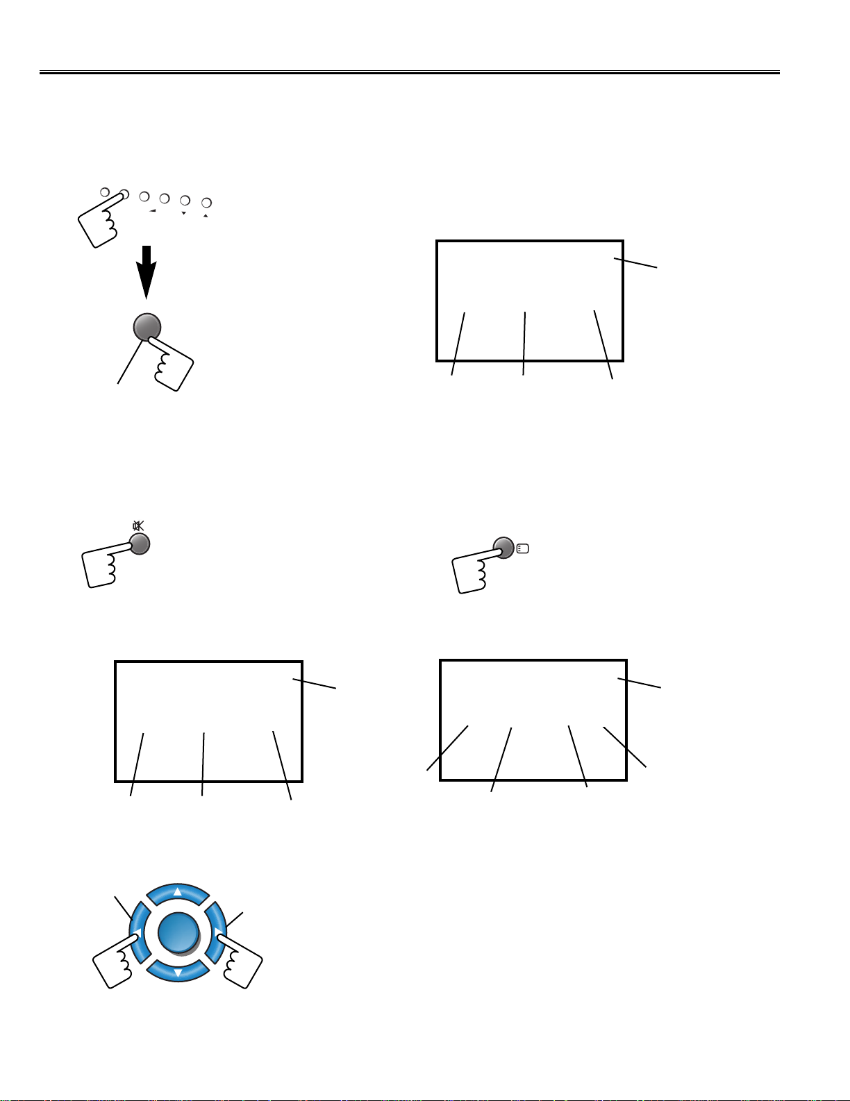
Horizontal centre
Vertical size
(1) Receive a crosshatch pattern.
(2) Select a picture mode of NATURAL by pressing the
PICTURE MODE button.
(3) Select [V S CORRECT 50] in the service mode.
(4) Adjust Vertical S-letter Correction so that the difference
of “c”, “d” and “e” becomes less than 2 mm by pressing
the VOLUME + or - button.
(5) Confirm Vertical Linearity and adjust Vertical Center
then Vertical Size.
(6) Exit from service mode.
Item 12 [V S CORRECT 50] V-S CORRECTION
(1) Receive a crosshatch pattern.
(2) Select a picture mode of NATURAL by pressing the
PICTURE MODE button.
(3) Select [V-LINEARITY 50] in the service mode.
(4) Adjust Vertical Linearity so that the difference of “a” and
“b” becomes less than 3mm by pressing VOLUME + or
- button.
(5) Exit from service mode.
Item 14 [V-LINEARITY 50] VERTICAL LINEARITY
(1) Receive a monochrome circular pattern.
(2) Set the brightness and contrast to normal.
(3) Select [V-SHIFT 50] in the service mode.
(4) Change value to be optimum verticall centre position.
(5) Exit from service mode.
Item 16 [V-SHIFT 50] VERTICAL CENTRE
Vertical centre
Upper
a
Center
b
Bottom
c
Upper
d
e
Center
Bottom
Page 16

-16-
Service Adjustments
Following adjustments are not required to readjust when replacing the memory IC.
Note: +B (+130V) Voltage Check and Grayscale Adjustment
must be completed before attempting High Voltage Check.
(1) Connect high voltage voltmeter negative lead to
ground, and connect + lead to anode of picture tube.
(2) Tune receiver to an active channel and confirm TV is
operating properly.
(3) Maximize the beam current by adjusting the contrast
and brightness controls to maximum. Confirm high
voltage is within 24.0 KV and 26.0 KV at maximum
beam current.
(4) Eliminate the beam current by adjusting the contrast
and brightness controls to minimum. Confirm high
voltage does not exceed 27.5 KV at zero beam current.
If reading is not within range, check horizontal circuit.
No high-voltage adjustment is provided on this chassis.
HIGH VOLTAGE CHECK
???
***
C611
C615
C661
D611
C691
3
4
2
1
D610
C629
R603
R604
R607
R610
IC601A
R631
R632
J294
C610
C613
D609
D613
R611
D637
R639
R606
R685
C612
VR631
C617
C632
L632
L602
R609
D612
J625
D614
D636
D686
C637
R692
IC601
C614A
C614
C616
8
1
7
T611A
1
9
8
T611
TP-B
C489
R605
T471H5
T611H10
T611AH9
T611H7
T611AH7
T611H1
T611AH4
T611H4
T611AH1
T471H4
T47
(1) Connect DC meter to TP-B and the ground.
(2) Tune the receiver to an active channel and synchro-
nized picture. Select NATURAL picture mode by pressing the PICTURE MODE button on the remote control.
(3) Adjust B-voltage to be 130 ± 0.5V DC by using VR631.
B-VOLTAGE SUPPLY CHECKING
(1) Receive the monochrome circular pattern.
(2) Set the brightness to normal and contrast to maximum.
(3) Adjust the focus control on the F.B.T. for the best focus
on the screen centre.
FOCUS ADJUSTMENT
MAIN BOARD
B-Voltage Supply Adjustment
MAIN BOARD
TP-B
C356
C435AH2
Focus VR
(Upper side)
VR631
R445
KDY-1
KDY-4
KDY-6
KDY-5
R103
635
T611H10
T611AH9
611A
R685
J625
D686
T611H4
T611H1
T611H7
KDY-3
D445
J606
J404
C631
JP482
D631
R435
R435H2
TP-B
R639
D637
J294
C691
C661
C489
VR631
R435H1
T471H5
T471H1
T471H2
T471H4
T471
C471
R423
R424
R355
T471H10
T471H7
Page 17

-17-
Special Function
1
To enter into the special function setting mode, press and
hold the MENU button of the TV set, then press the
Recall button on the Remote Control.
Once TUNING LOCK is switched on, further channel tuning
(Pre-set) is not possible. The Channel Swapping function also
is not possible.
2
Select an item of the special functions by pressing the
PROGRAMME UP or DOWN button on the remote control
or the TV set.
3
Set the selected special function “ ON “ by pressing the
VOLUME + or -button. To cancel, set to “ OFF”.
(2) Tuning Lock setting
The following special functions can be set up on this TV
set.
With this function, a maximum sound volume limit can be set at
any level.
(3) Music Mode setting
When Music Mode is ON, Programme position from “247” to
“255” and “0” are set Music Mode. Only sound is provided and
any picture is not on the screen under Music Mode.
Set AV-START to ON and every time the TV set is switched on,
AV1 position will be the initial programme position.
(4) AV Start setting
TUNING LOCKED
How to set the special function:
Note: When making the VOLUME LOCK setting, set the
desired maximum sound volume by pressing the VOLUME + or
-
button before entering Special Function setting mode.
AV1
MUSIC
Turns black
screen
4
Press the MENU button of the remote control to return to
the normal TV mode.
(1) Volume Lock setting
T
OCK
T
OCK
MENU
MENU
BASS EXPANDER ON
SOUND
TV/AV
M
E
N
U
- +
CH
VOLUME LOCK
TUNING LOCK
MUSIC MODE
AV START
SELECT ADJUST
VOLUME LOCK
UNING L
MUSIC MODE
AV START
OFF
OFF
OFF
OFF
OFF
OFF
OFF
OFF
M
EXIT
SELECT ADJUST
VOLUME LOCK
UNING L
MUSIC MODE
AV START
SELECT ADJUST
OFF
ON
OFF
OFF
MENU
M
EXIT
M
EXIT
Page 18

-18-
Purity and Convergence Adjustment
RED
BLUE
Adjust tabs together to
superimpose red and
blue horizontal line.
Figure- 2 BLUE AND RED LINE MOVEMENT
Figure- 3 BLUE/RED AND GREEN MOVEMENT
Adjust tabs together to
superimpose red/blue
and green horizontal
line.
Adjust tabs angle to superimpose
blue and red vertical line.
Adjust tabs angle to superimpose
red/blue and green vertical line.
GREEN
BLUE / RED
CAUTION: The Convergence and Purity adjustments have been made at the factory. Readjustment
should be made only after picture tube or deflection yoke replacement, following the steps below:
PURITY ADJUSTMENT
1. Demagnetize the picture tube and receiver using an external
degaussing coil. When replacing picture tube or deflection
yoke, mount deflection yoke and purity-convergence magnets
assembly properly, see figures 1 and 4.
2. Turn Red and Blue guns off and provide only Green raster.
Rotate Screen control to fully counterclockwise. Rotate Red
and Blue Bias controls fully counterclockwise. Slowly rotate
Green Bias control clockwise to produce Green raster.
3. Loosen the screw holding the Deflection Yoke and remove the
3 Rubber Wedges, and slide the Deflection Yoke fully forward.
4. Rotate and spread the Tabs of the two Purity Magnets to centre the vertical green belt in the picture screen. The Purity
Magnets are also adjusted to obtain vertical centring of the
raster.
5. Slowly slide the Deflection Yoke backward until a uniform
green screen is obtained.
6. Check the purity of the red and blue screens for uniformity,
turn off other colours to check this (use bias controls).
Readjust the yoke position if necessary until all screens are
pure.
7. Adjust each Bias control and screen control to obtain white
raster. Refer to Gray Scale Adjustment. If part of the picture
screen is coloured, adjust the Deflection Yoke position forward
or backward slightly.
8. Tighten the mounting screw of the Deflection Yoke. Adjust
Convergence next.
CENTRE CONVERGENCE ADJUSTMENT
1. Use a dot crosshatch pattern signal.
2. Turn Red and Blue guns on and turn off Green gun. Adjust the
angle between the Tabs of the Four Pole Magnet 1 and 2, and
superimpose the Red and Blue vertical lines in the centre area
of the picture screen. Refer to figure 2.
3. Keeping the mutual angle of the Tabs of the Four Pole Magnet
turn them together to superimpose the Blue and Red horizontal lines in the centre area of the picture screen. Refer to figure 2.
4. Turn Green gun on and adjust Six Pole Magnet 3 and 4 that
the Green line superimposed on the Red/Blue lines.
This is the same procedure used in steps 2 and 3.
Refer to figure 3.
OUTER AREA CONVERGENCE ADJUSTMENT
Slightly loosen the screw holding the Deflection Yoke. Adjust the
Deflection Yoke to converge the detail in the outer area (left side
and right side) of the picture screen by orbital movement of the
front of the Yoke, then secure the Deflection Yoke in appropriate
position by putting the wedges as illustrated. Tighten screw holding the Deflection Yoke.
Figure 4. Deflection Yoke Movement
Figure 1. Purity and Convergence Magnets
Figure 5. Adjusting Magnet
Note: The form of deflection yoke changes with models.
PURITY
MAGNET
TABS
SIX-POLE
MAGNET TABS
4
3
1
2
FOUR-POLE
MAGNET TABS
ANGLE
OF TABS
FOCUS GAP
(G3-G4)
DEFLECTION YOKE
DEFLECTION YOKE
MOUNTING SCREW
RUBBER
WEDGE
ANGLE OF MAGNET TABS
MAGNET TABS
Page 19

-19-
Mechanical Disassembly
CABINET BACK REMOVAL
1. Refer to Figure 1, remove 7 screws.
2. Pull off cabinet back and remove.
Figure 1. Cabinet Back Removal
When an abnormality occurs during TV reception, it causes pin 72 of the Processor to go continually Low (less
than 2.0V) for about 2 second. The Processor detects that this has occurred and outputs the signal from pin 74 to
switch off the power supply lines.
Releasing the protective circuit and restoring power supply
To release the protective circuit and restore power supply, turn the power to the TV set OFF and then ON again via
either the main power switch or the ON-OFF button on the remote control. This will work only if the power supply
trouble was temporary. If there is permanent trouble such as a damaged circuit, power cannot be restored and the
circuit will have to be repaired.
This TV set has a built-in power supply protection circuit.
It is provided to protect the TV set in case of a power supply circuit malfunctions. When something abnormality occurs
during TV reception, the TV set goes to the stand-by mode.
Protection Circuit
INPUT
MONITOR
OUT
AV1/DVD
AUDIO
R
R
C
R
L
L
C
B
ANT. 75Ω
V
I
D
Y
E
O
S-VIDEO
VIDEO
Page 20

-20-
Note: Parts order must contain Service Ref. No., Part No., and descriptions.
1 610 331 7175 BUTTON POWER-BB2A
610 229 8406 SPRING-E3HA
(for power button)
2 610 331 7274 DEC IND-BB2A
3 610 331 7380 BUTTON UNITED-BB2A
4 610 335 2978 CABINET FRONT-BD6A
5 645 069 2185 BADGE,SANYO*43.5X10L43.5
6 610 335 3012 CABINET BACK-BD6A
7 652 002 0634 REMOCON,JXPSG
8 610 313 3393 RC-BATTERY LID-JXPLA
610 335 3050 INSTRUCTION MANUAL-C8WC
610 338 0674 CORRECTION NOTICE-C8WM
610 335 3104 SCHEMATIC DIAGRAM-C8WC
Key No. Part No. Description Key No. Part No. Description
6
8
Cabinet Parts List
BD6B
1
2
3
5
4
7
INPUT
MONITOR
OUT
AV1/DVD
AUDIO
R
R
C
R
L
L
C
B
ANT. 75Ω
V
I
D
Y
E
O
S-VIDEO
VIDEO
TV
/AV
V
I
D
E
M
O
E
N
U
L
-
A
U
D
-
I
O
-
R
+
C
H
PO
W
ER
TV/AV
TIMER
x
3
2
1
56
4
9
8
7
PP
-/--
0
CH
CH SCAN
SWAP
MENU
.
CH
A B
SOUND
S. SYS
BASS
JXPSC
PICTURE
SURROUND
Page 21

-21-
BD6B
OUT OF CIRCUIT BOARD
PICTURE TUBE
Q901 4140147809 CRT ASSY A51QDX993X005(A)
Q901-1 6450088674 MAGNET,CG.PR
6450867484 MAGNET,CG,PR
Q901-2A 6101170154 DY SPACER-D4AK
6102337891 DY SPACER E2HA
6102904154 DY SPACER-F8LZ
Q901-2B 6101170154 DY SPACER-D4AK
6102337891 DY SPACER E2HA
6102904154 DY SPACER-F8LZ
Q901-2C 6101170154 DY SPACER-D4AK
6102337891 DY SPACER E2HA
6102904154 DY SPACER-F8LZ
COIL
L901 6450837616 ASSY,COIL,DEGAUSSING
MISCELLANEOUS
SP901 6520014831 SPEAKER,8
6520018174 SPEAKER,8
SP902 6520014831 SPEAKER,8
6520018174 SPEAKER,8
W901 6450956287 CORD,POWER-2.0MK-W-A5063
W902 6102837179 ASSY,WIRE GND CONNECTOR C
6103366463 ASSY,PWB,MAIN BD6B
1AA0B10S251JA
TRANSISTOR
Q1001 4051648016 TR KTA1504S-GR-RTK
4051345925 TR 2SA1037AK-T146-R
4051472215 TR 2SA1037AK-S-T146
4050020318 TR 2SA1037K T146 R
4050020417 TR 2SA1037K T146 S
4050026726 TR 2SA1179-M6-TB
4050026924 TR 2SA1179-M7-TB
4051631513 TR 2SA1179N-M6-TB
4051739615 TR 2SA1235A1E
4051739714 TR 2SA1235A1F
Q1002 4051648016 TR KTA1504S-GR-RTK
4051345925 TR 2SA1037AK-T146-R
4051472215 TR 2SA1037AK-S-T146
4050020318 TR 2SA1037K T146 R
4050020417 TR 2SA1037K T146 S
4050026726 TR 2SA1179-M6-TB
4050026924 TR 2SA1179-M7-TB
4051631513 TR 2SA1179N-M6-TB
4051739615 TR 2SA1235A1E
4051739714 TR 2SA1235A1F
Q1003 4051648412 TR KTC3875S-GR-RTK
4050144519 TR 2SC2412K T146 R
4050144618 TR 2SC2412K T146 S
4050158724 TR 2SC2812-L6-TB
!
!
!
Chassis Electrical Parts List
Ref. No. Part No. Description Ref. No. Part No. Description
Product safety should be considered when a component replacement is made in any area of a receiver.
Components indicated by a mark in this parts list and the circuit diagram show components whose value have
special significance to product safety. It is particularly recommended that only parts specified on the following parts
list be used for components replacement pointed out by the mark.
!
Note: Parts order must contain Service Ref. No., Part No., and descriptions. The main PCB unit will be supplied without tuner and
flyback transformer. They should be ordered separately.
NOTES:
Read description in the Capacitor and Resistor as follows:
CAPACITOR
CERAMIC 100P K 50V
Rated Voltage
Tolerance Symbols:
Less than 10pF
A : Not specified B : ±0.1pF C : ±0.25pF
D : ±0.5pF F : ±1PF G : ±2pF
R : ±0.25-0pF S : ±0-0.25pF E : +0-1pF
More than 10pF
A : Not specified B : ±0.1% C : ±0.25%
D : ±0.5% F : ±1% G : ±2%
H : ±3% J : ±5% K : ±10%
L : ±15% M : ±20% N : ±30%
P : +100-0% Q : +30-10% T : +50-10%
U : +75-10% V : +20-10% W : +100-10%
X : +40-20% Y : +150-10% Z : +80-20%
Rated value: P=pico farad, U=micro farad
Material:
CERAMIC........... Ceramic
MT-PAPER......... Metallized Paper
POLYESTER...... Polyester
MT-POLYEST.....Metallized Polyester
POLYPRO.......... Polypropylene
MT-POLYPRO.... Metallized Polypropylene
COMPO FILM..... Composite film
MT-COMPO........ Metallized Composite
STYRENE........... Styrene
TA-SOLID........... Tantalum Solid
AL-SOLID........... Aluminium Solid
ELECT................ Electrolytic
NP-ELECT.......... Non-polarised Electrolytic
OS-SOLID.......... Aluminium Solid with Organic Semiconductive Electrolytic
DL-ELECT.......... Double Layered Electrolytic
RESISTOR
CARBON 4.7K J A 1/4W
Rated Wattage
Performance Symbols:
A: General B: Non flammable Z: Low noise
Other: Temperature coefficient
Tolerance Symbols:
A: ±0.05% B: ±0.1% C: ±0.25% D: ±0.5%
F: ±1% G: ±2% J: ±5% K: ±10%
M: ±20% P: +5-15%
Rated value, ohms:
K: 1,000, M: 1,000,000
Material:
CARBON........... Carbon
MT-FILM............ Metal Film
OXIDE-MT......... Oxide Metal Film
SOLID................ Composition
MT-GLAZE......... Metal Glaze
WIRE WOUND... Wire Wound
CERAMIC RES.. Ceramic
FUSIBLE RES.... Fusible
Page 22

-22-
BD6B
4050158922 TR 2SC2812-L7-TB
4051631612 TR 2SC2812N-L6-TB0
4051739813 TR 2SC3928A1R
4051739912 TR 2SC3928A1S
Q111 4052187712 TR KTC3879S-Y
4050159721 TR 2SC2814-F4-TB
Q1901 4051648412 TR KTC3875S-GR-RTK
4050144519 TR 2SC2412K T146 R
4050144618 TR 2SC2412K T146 S
4050158724 TR 2SC2812-L6-TB
4050158922 TR 2SC2812-L7-TB
4051631612 TR 2SC2812N-L6-TB0
4051739813 TR 2SC3928A1R
4051739912 TR 2SC3928A1S
Q201 4050235009 TR 2SD400-E-MP
Q202 4050235009 TR 2SD400-E-MP
Q203 4050235009 TR 2SD400-E-MP
Q206 4050235009 TR 2SD400-E-MP
Q431 4050180517 TR 2SC3332-R
4050180606 TR 2SC3332-S
Q432 4060171908 TR TT2140LS-YB11
Q471 4050036002 TR 2SA1319-S
Q472 4051648412 TR KTC3875S-GR-RTK
4050144519 TR 2SC2412K T146 R
4050144618 TR 2SC2412K T146 S
4050158724 TR 2SC2812-L6-TB
4050158922 TR 2SC2812-L7-TB
4051631612 TR 2SC2812N-L6-TB0
4051739813 TR 2SC3928A1R
4051739912 TR 2SC3928A1S
Q511 4051648412 TR KTC3875S-GR-RTK
4050144519 TR 2SC2412K T146 R
4050144618 TR 2SC2412K T146 S
4050158724 TR 2SC2812-L6-TB
4050158922 TR 2SC2812-L7-TB
4051631612 TR 2SC2812N-L6-TB0
4051739813 TR 2SC3928A1R
4051739912 TR 2SC3928A1S
Q631 4051648412 TR KTC3875S-GR-RTK
4050144519 TR 2SC2412K T146 R
4050144618 TR 2SC2412K T146 S
4050158724 TR 2SC2812-L6-TB
4050158922 TR 2SC2812-L7-TB
4051631612 TR 2SC2812N-L6-TB0
4051739813 TR 2SC3928A1R
4051739912 TR 2SC3928A1S
Q632 4051648412 TR KTC3875S-GR-RTK
4050144519 TR 2SC2412K T146 R
4050144618 TR 2SC2412K T146 S
4050158724 TR 2SC2812-L6-TB
4050158922 TR 2SC2812-L7-TB
4051631612 TR 2SC2812N-L6-TB0
4051739813 TR 2SC3928A1R
4051739912 TR 2SC3928A1S
Q683 4052197711 TR KTB985-B-AT/P
4050890000 TR 2SA1707-S
4050890109 TR 2SA1707-T
4050096907 TR 2SB985-S
Q684 4051648412 TR KTC3875S-GR-RTK
4050144519 TR 2SC2412K T146 R
4050144618 TR 2SC2412K T146 S
4050158724 TR 2SC2812-L6-TB
4050158922 TR 2SC2812-L7-TB
4051631612 TR 2SC2812N-L6-TB0
4051739813 TR 2SC3928A1R
4051739912 TR 2SC3928A1S
Q801 4050235009 TR 2SD400-E-MP
Q802 4051648016 TR KTA1504S-GR-RTK
4051345925 TR 2SA1037AK-T146-R
4051472215 TR 2SA1037AK-S-T146
4050020318 TR 2SA1037K T146 R
4050020417 TR 2SA1037K T146 S
4050026726 TR 2SA1179-M6-TB
4050026924 TR 2SA1179-M7-TB
4051631513 TR 2SA1179N-M6-TB
4051739615 TR 2SA1235A1E
4051739714 TR 2SA1235A1F
Q886 4051648412 TR KTC3875S-GR-RTK
4050144519 TR 2SC2412K T146 R
4050144618 TR 2SC2412K T146 S
4050158724 TR 2SC2812-L6-TB
4050158922 TR 2SC2812-L7-TB
4051631612 TR 2SC2812N-L6-TB0
4051739813 TR 2SC3928A1R
4051739912 TR 2SC3928A1S
INTEGRATED CIRCUIT
IC001 4096827701 IC LA42205-E
IC1200 4096803012 IC R2S15900SP
IC201 4106363304 IC R2J12203M4-XXXFP
IC501 4096646104 IC LA78040B-E
IC601 4106062108 IC STR-W6753(LF2003
IC802 4096760701 IC LE24C161-E-C
4104958007 IC AT24C16A-10PU-2.7
4106374607 IC LE24C162-E
4094594506 IC 24LC16B/P
CAPACITOR
C001 4041064106 ELECT 1000U M 25V
4031904702 ELECT 1000U M 25V
C002 4041080403 ELECT 100U M 16V
4041081509 ELECT 100U M 25V
4032112918 ELECT 100U M 16V
4031905214 ELECT 100U M 25V
C003 4041046409 CERAMIC 3900U K 50V
4040914204 CERAMIC 3900P K 50V
4031577213 CERAMIC 3900P K 50V
C004 4041140206 CERAMIC 1U Z 16V
4032070317 CERAMIC 1U Z 16V
4032789615 CERAMIC 1U Z 16V
C005 4041140206 CERAMIC 1U Z 16V
4032070317 CERAMIC 1U Z 16V
4032789615 CERAMIC 1U Z 16V
C006 4041046409 CERAMIC 3900U K 50V
4040914204 CERAMIC 3900P K 50V
4031577213 CERAMIC 3900P K 50V
C011 4041081202 ELECT 10U M 16V
4041151707 ELECT 10U M 50V
4032113519 ELECT 10U M 50V
C1001 4040970101 ELECT 1U M 50V
4040843801 ELECT 1U M 50V
C1004 4040970200 ELECT 10U M 50V
4040843900 ELECT 10U M 50V
C1005 4040970200 ELECT 10U M 50V
4040843900 ELECT 10U M 50V
C1006 4040988403 ELECT 470U M 10V
4040842606 ELECT 470U M 10V
C1009 4040970101 ELECT 1U M 50V
4040843801 ELECT 1U M 50V
C101 4040987802 ELECT 470U M 6.3V
4040842408 ELECT 470U M 6.3V
C1010 4041044900 CERAMIC 0.1U K 50V
4040912606 CERAMIC 0.1U K 50V
4033670417 CERAMIC 0.1U K 50V
Ref. No. Part No. Description Ref. No. Part No. Description
Page 23

C1011 4041044900 CERAMIC 0.1U K 50V
4040912606 CERAMIC 0.1U K 50V
4033670417 CERAMIC 0.1U K 50V
C1012 4040970101 ELECT 1U M 50V
4040843801 ELECT 1U M 50V
C104 4040973607 ELECT 47U M 50V
4040844303 ELECT 47U M 50V
C106 4040973201 ELECT 22U M 50V
4040873006 ELECT 22U M 50V
C111 4041032907 CERAMIC 0.01U K 50V
4040901204 CERAMIC 0.01U K 50V
4032152211 CERAMIC 0.01U K 50V
C112 4041032907 CERAMIC 0.01U K 50V
4040901204 CERAMIC 0.01U K 50V
4032152211 CERAMIC 0.01U K 50V
C114 4041032907 CERAMIC 0.01U K 50V
4040901204 CERAMIC 0.01U K 50V
4032152211 CERAMIC 0.01U K 50V
C115 4040972808 ELECT 0.47U M 50V
4040843702 ELECT 0.47U M 50V
C1201 4040988205 ELECT 2200U M 10V
4040854906 ELECT 2200U M 10V
C1202 4041044900 CERAMIC 0.1U K 50V
4040912606 CERAMIC 0.1U K 50V
4033670417 CERAMIC 0.1U K 50V
C1204 4041047000 CERAMIC 0.056U K 50V
4040914808 CERAMIC 0.056U K 50V
4033082111 CERAMIC 0.056U K 16V
4033565218 CERAMIC 0.056U K 50V
C1205 4041047000 CERAMIC 0.056U K 50V
4040914808 CERAMIC 0.056U K 50V
4033082111 CERAMIC 0.056U K 16V
4033565218 CERAMIC 0.056U K 50V
C1206 4041045402 CERAMIC 1800P K 50V
4040913009 CERAMIC 1800P K 50V
4031577015 CERAMIC 1800P K 50V
4032355513 CERAMIC 1800P K 50V
C1207 4040973409 ELECT 4.7U M 50V
4040844204 ELECT 4.7U M 50V
C1208 4041045402 CERAMIC 1800P K 50V
4040913009 CERAMIC 1800P K 50V
4031577015 CERAMIC 1800P K 50V
4032355513 CERAMIC 1800P K 50V
C1209 4041047000 CERAMIC 0.056U K 50V
4040914808 CERAMIC 0.056U K 50V
4033082111 CERAMIC 0.056U K 16V
4033565218 CERAMIC 0.056U K 50V
C1210 4040952602 CERAMIC 0.22U Z 16V
4040913405 CERAMIC 0.22U K 50V
4032812412 CERAMIC 0.22U K 16V
C1211 4041045303 CERAMIC 0.015U K 50V
4040912903 CERAMIC 0.015U K 50V
4030709813 CERAMIC 0.015U K 50V
4032152419 CERAMIC 0.015U K 50V
C1212 4040973409 ELECT 4.7U M 50V
4040844204 ELECT 4.7U M 50V
C1213 4041047000 CERAMIC 0.056U K 50V
4040914808 CERAMIC 0.056U K 50V
4033082111 CERAMIC 0.056U K 16V
4033565218 CERAMIC 0.056U K 50V
C1216 4040970200 ELECT 10U M 50V
4040843900 ELECT 10U M 50V
C1217 4040970101 ELECT 1U M 50V
4040843801 ELECT 1U M 50V
C1218 4040970101 ELECT 1U M 50V
4040843801 ELECT 1U M 50V
C1221 4033588316 CERAMIC 1U K 10V
4033456615 CERAMIC 1U M 10V
C1222 4033588316 CERAMIC 1U K 10V
4033456615 CERAMIC 1U M 10V
C1223 4033588316 CERAMIC 1U K 10V
4033456615 CERAMIC 1U M 10V
C1224 4033588316 CERAMIC 1U K 10V
4033456615 CERAMIC 1U M 10V
C1225 4033588316 CERAMIC 1U K 10V
4033456615 CERAMIC 1U M 10V
C1226 4033588316 CERAMIC 1U K 10V
4033456615 CERAMIC 1U M 10V
C1228 4033588316 CERAMIC 1U K 10V
4033456615 CERAMIC 1U M 10V
C124 4040970101 ELECT 1U M 50V
4040843801 ELECT 1U M 50V
C125 4040972808 ELECT 0.47U M 50V
4040843702 ELECT 0.47U M 50V
C126 4032002625 ELECT 0.47U M 50V
C127 4041040209 CERAMIC 100P J 50V
4040946403 CERAMIC 100P J 50V
4031573611 CERAMIC 100P J 50V
C1902 4040973201 ELECT 22U M 50V
4040873006 ELECT 22U M 50V
C201 4041159109 MT-POLYEST 0.22U J 63V
4040935407 MT-POLYEST 0.22U J 63V
4032377901 MT-COMPO 0.22U J 50V
C202 4041044900 CERAMIC 0.1U K 50V
4040912606 CERAMIC 0.1U K 50V
4033670417 CERAMIC 0.1U K 50V
C203 4040947004 CERAMIC 15P J 50V
4031554214 CERAMIC 15P J 50V
C204 4040970408 ELECT 47U M 35V
4040854609 ELECT 47U M 35V
C205 4040970101 ELECT 1U M 50V
4040843801 ELECT 1U M 50V
C206 4041044900 CERAMIC 0.1U K 50V
4040912606 CERAMIC 0.1U K 50V
4033670417 CERAMIC 0.1U K 50V
C207 4041045303 CERAMIC 0.015U K 50V
4040912903 CERAMIC 0.015U K 50V
4032152419 CERAMIC 0.015U K 50V
C208 4040984009 MT-POLYEST 0.1U J 63V
4040852902 MT-POLYEST 0.1U J 63V
4032378007 MT-COMPO 0.1U J 50V
C209 4041159109 MT-POLYEST 0.22U J 63V
4040935407 MT-POLYEST 0.22U J 63V
4032377901 MT-COMPO 0.22U J 50V
C211 4041044900 CERAMIC 0.1U K 50V
4040912606 CERAMIC 0.1U K 50V
4033670417 CERAMIC 0.1U K 50V
C212 4041081301 ELECT 47U M 16V
4041174607 ELECT 47U M 25V
4041157204 ELECT 47U M 35V
4031904811 ELECT 47U M 25V
4032118217 ELECT 47U M 35V
C213 4040972808 ELECT 0.47U M 50V
4040843702 ELECT 0.47U M 50V
C214 4041045303 CERAMIC 0.015U K 50V
4040912903 CERAMIC 0.015U K 50V
4032152419 CERAMIC 0.015U K 50V
C215 4040984009 MT-POLYEST 0.1U J 63V
4040852902 MT-POLYEST 0.1U J 63V
4032378007 MT-COMPO 0.1U J 50V
C216 4041032907 CERAMIC 0.01U K 50V
4040901204 CERAMIC 0.01U K 50V
4032152211 CERAMIC 0.01U K 50V
C218 4041032907 CERAMIC 0.01U K 50V
-23-
BD6B
Ref. No. Part No. Description Ref. No. Part No. Description
Page 24

-24-
BD6B
4040901204 CERAMIC 0.01U K 50V
4032152211 CERAMIC 0.01U K 50V
C219 4040970408 ELECT 47U M 35V
4040854609 ELECT 47U M 35V
C220 4040970408 ELECT 47U M 35V
4040854609 ELECT 47U M 35V
C221 4041032907 CERAMIC 0.01U K 50V
4040901204 CERAMIC 0.01U K 50V
4032152211 CERAMIC 0.01U K 50V
C222 4040970200 ELECT 10U M 50V
4040843900 ELECT 10U M 50V
C223 4041151707 ELECT 10U M 50V
4032113519 ELECT 10U M 50V
C224 4040970200 ELECT 10U M 50V
4040843900 ELECT 10U M 50V
C225 4040970200 ELECT 10U M 50V
4040843900 ELECT 10U M 50V
C231 4041044900 CERAMIC 0.1U K 50V
4040912606 CERAMIC 0.1U K 50V
4033670417 CERAMIC 0.1U K 50V
C232 4040970101 ELECT 1U M 50V
4040843801 ELECT 1U M 50V
C233 4041044900 CERAMIC 0.1U K 50V
4040912606 CERAMIC 0.1U K 50V
4033670417 CERAMIC 0.1U K 50V
C234 4041045709 CERAMIC 2200U K 50V
4040913306 CERAMIC 2200P K 50V
4031134119 CERAMIC 2200P K 50V
C235 4041044900 CERAMIC 0.1U K 50V
4040912606 CERAMIC 0.1U K 50V
4033670417 CERAMIC 0.1U K 50V
C239 4011506011 MT-GLAZE 0.000 ZA 1/10W
4011057919 MT-GLAZE 0.000 ZA 1/16W
C240 4011506011 MT-GLAZE 0.000 ZA 1/10W
4011057919 MT-GLAZE 0.000 ZA 1/16W
C241 4011506011 MT-GLAZE 0.000 ZA 1/10W
4011057919 MT-GLAZE 0.000 ZA 1/16W
C242 4011506011 MT-GLAZE 0.000 ZA 1/10W
4011057919 MT-GLAZE 0.000 ZA 1/16W
C243 4011506011 MT-GLAZE 0.000 ZA 1/10W
4011057919 MT-GLAZE 0.000 ZA 1/16W
C246 4041032907 CERAMIC 0.01U K 50V
4040901204 CERAMIC 0.01U K 50V
4032152211 CERAMIC 0.01U K 50V
C432 4041135103 CERAMIC 3900P K 500V
4032753329 CERAMIC 3900P K 500V
C433 4041135103 CERAMIC 3900P K 500V
4032753329 CERAMIC 3900P K 500V
C434 4041085705 ELECT 330U M 35V
4041075201 ELECT 330U M 35V
C435 4040831709 MT-POLYPRO 6000P H 1.5K
4041021505 MT-POLYPRO 6000P H 1.5V
4041165001 MT-POLYPRO 6000P J 1.6K
4033727319 MT-POLYPRO 6000P H 1.5K
C436 4041124206 CERAMIC 270P K 3K
4041165209 CERAMIC 270P K 2K
4041165100 CERAMIC 270P K 2K
4032690416 CERAMIC 270P K 3K
C438 4041124206 CERAMIC 270P K 3K
4041165209 CERAMIC 270P K 2K
4041165100 CERAMIC 270P K 2K
4032690416 CERAMIC 270P K 3K
C441 4040850205 MT-POLYPRO 0.27U J 250V
4033467126 MT-POLYPRO 0.27U J 250V
4033794311 MT-POLYPRO 0.27U J 250V
4033726817 MT-POLYPRO 0.27U J 250V
C471 4040565307 NP-ELECT 2.2U M 100V
4041089000 NP-ELECT 2.2U M 100V
4040849902 NP-ELECT 2.2U M 100V
C486 4041054701 ELECT 22U M 250V
4034553610 ELECT 22U M 250V
4034320806 ELECT 22U M 250V
C489 4041137107 MT-POLYEST 0.47U J 250V
4030666106 MT-POLYEST 0.47U J 250V
4034335008 MT-POLYEST 0.47U J 250V
C491 4041136803 CERAMIC 680P K 500V
4034164915 CERAMIC 680P K 500V
C511 4041151707 ELECT 10U M 50V
4032113519 ELECT 10U M 50V
C514 4041151707 ELECT 10U M 50V
4032113519 ELECT 10U M 50V
C515 4041064106 ELECT 1000U M 25V
4031904702 ELECT 1000U M 25V
C517 4041157303 ELECT 220U M 35V
4032114427 ELECT 220U M 35V
C518 4030575329 POLYESTER 1200P J 50V
4031793702 POLYESTER 1200P J 50V
4030704937 CERAMIC 1200P K 50V
C521 4041063505 ELECT 1000U M 35V
4032112532 ELECT 1000U M 35V
C524 4041155606 POLYESTER 0.068U J 100V
4033074017 POLYESTER 0.068U J 100V
4031429522 POLYESTER 0.068U K 100V
4032890826 POLYESTER 0.068U K 100V
C525 4041040209 CERAMIC 100P J 50V
4040946403 CERAMIC 100P J 50V
4031573611 CERAMIC 100P J 50V
C601 4040881704 MT-POLYEST 0.22U K 250V
4040888802 MT-POLYEST 0.22U M 275V
4040941804 MT-POLYEST 0.22U K 275V
4040966708 MT-POLYPRO 0.22U M 275V
C602 4040881704 MT-POLYEST 0.22U K 250V
4040888802 MT-POLYEST 0.22U M 275V
4040941804 MT-POLYEST 0.22U K 275V
4040966708 MT-POLYPRO 0.22U M 275V
C603 4041157501 CERAMIC 1000P K 1K
4041078400 CERAMIC 1000P K 1K
4041157105 CERAMIC 1000P K 1K
4040846307 CERAMIC 1000P K 1K
4030766707 CERAMIC 1000P K 1K
4032221313 CERAMIC 1000P K 1K
4032719622 CERAMIC 1000P K 1K
C604 4041157501 CERAMIC 1000P K 1K
4041078400 CERAMIC 1000P K 1K
4041157105 CERAMIC 1000P K 1K
4040846307 CERAMIC 1000P K 1K
4030766707 CERAMIC 1000P K 1K
4032221313 CERAMIC 1000P K 1K
4032719622 CERAMIC 1000P K 1K
C605 4041036905 CERAMIC 0.1U K 25V
4040950806 CERAMIC 0.1U K 25V
4033423310 CERAMIC 0.1U K 25V
4031640214 CERAMIC 0.1U Z 25V
4033670417 CERAMIC 0.1U K 50V
4033053517 CERAMIC 0.1U Z 50V
C607 4041048304 ELECT 220U M 400V
4041107100 ELECT 150U M 400V
C610 4040904601 POLYESTER 2200P K 63V
4041154203 POLYESTER 2200P J 100
4031792705 POLYESTER 2200P J 50V
4031792606 POLYESTER 2200P K 50V
4032770019 POLYESTER 2200P K 100V
C611 4041155200 ELECT 1U M 50V
4032112116 ELECT 1U M 50V
!
!
Ref. No. Part No. Description Ref. No. Part No. Description
Page 25

C612 4030572130 POLYESTER 0.1U J 50V
4031818306 POLYESTER 0.1U J 50V
4030573107 POLYESTER 0.1U K 50V
4031818207 POLYESTER 0.1U K 50V
C613 4041155507 POLYESTER 6800P J 100V
4031790404 POLYESTER 6800P J 50V
4031790305 POLYESTER 6800P K 50V
C614 4040869900 POLYPRO 0.022U J 630V
4030840318 POLYPRO 0.022U J 630V
C615 4041162406 ELECT 33U M 35V
4032116015 ELECT 33U M 35V
C616 4041119707 CERAMIC 470P K 2K
4041126804 CERAMIC 470P K 2K
4041112500 CERAMIC 470P K 2K
4040862109 CERAMIC 470P K 2K
C617 4041093700 CERAMIC 390P K 3K
4040862406 CERAMIC 390P K 3K
4040850809 CERAMIC 390P K 3K
4033242505 CERAMIC 390P K 3K
4032758423 CERAMIC 390P K 3K
C627 4040733904 CERAMIC 1000P K 250V
4040732105 CERAMIC 1000P M 250V
4040713302 CERAMIC 1000P M 400V
4041113903 CERAMIC 1000P M 400V
4041039104 CERAMIC 1000P M 400V
C628 4040733904 CERAMIC 1000P K 250V
4040732105 CERAMIC 1000P M 250V
4040713302 CERAMIC 1000P M 400V
4041113903 CERAMIC 1000P M 400V
4041039104 CERAMIC 1000P M 400V
C629 4040733904 CERAMIC 1000P K 250V
4040732105 CERAMIC 1000P M 250V
4040713302 CERAMIC 1000P M 400V
4041113903 CERAMIC 1000P M 400V
4041039104 CERAMIC 1000P M 400V
C631 4041157501 CERAMIC 1000P K 1K
4041078400 CERAMIC 1000P K 1K
4041157105 CERAMIC 1000P K 1K
4040846307 CERAMIC 1000P K 1K
4030766707 CERAMIC 1000P K 1K
4032221313 CERAMIC 1000P K 1K
4032719622 CERAMIC 1000P K 1K
C632 4041078202 CERAMIC 470P K 1K
4040861508 CERAMIC 470P K 1K
4032475003 CERAMIC 470P K 1K
C633 4041078202 CERAMIC 470P K 1K
4040861508 CERAMIC 470P K 1K
4032475003 CERAMIC 470P K 1K
C634 4041078202 CERAMIC 470P K 1K
4040861508 CERAMIC 470P K 1K
4032475003 CERAMIC 470P K 1K
C637 4041139804 CERAMIC 150P K 50V
4031037529 CERAMIC 150P K 50V
C641 4040739005 ELECT 220U M 160V
4040973706 ELECT 220U M 160V
C643 4041080809 ELECT 470U M 35V
4032119620 ELECT 470U M 35V
C644 4041064106 ELECT 1000U M 25V
4031904702 ELECT 1000U M 25V
C645 4041063604 ELECT 2200U M 25V
4032115127 ELECT 2200U M 25V
C662 4041081509 ELECT 100U M 25V
4031905214 ELECT 100U M 25V
C801 4041032907 CERAMIC 0.01U K 50V
4040901204 CERAMIC 0.01U K 50V
4032152211 CERAMIC 0.01U K 50V
C802 4041032907 CERAMIC 0.01U K 50V
4040901204 CERAMIC 0.01U K 50V
4032152211 CERAMIC 0.01U K 50V
C803 4041032402 CERAMIC 1000P K 50V
4040901105 CERAMIC 1000P K 50V
4031133815 CERAMIC 1000P K 50V
C804 4041032907 CERAMIC 0.01U K 50V
4040901204 CERAMIC 0.01U K 50V
4032152211 CERAMIC 0.01U K 50V
C805 4040970408 ELECT 47U M 35V
4040854609 ELECT 47U M 35V
C806 4040970408 ELECT 47U M 35V
4040854609 ELECT 47U M 35V
C807 4041032907 CERAMIC 0.01U K 50V
4040901204 CERAMIC 0.01U K 50V
4032152211 CERAMIC 0.01U K 50V
C808 4041032907 CERAMIC 0.01U K 50V
4040901204 CERAMIC 0.01U K 50V
4032152211 CERAMIC 0.01U K 50V
C809 4040970408 ELECT 47U M 35V
4040854609 ELECT 47U M 35V
C810 4040947608 CERAMIC 22P J 50V
4031459915 CERAMIC 22P J 50V
C811 4041032907 CERAMIC 0.01U K 50V
4040901204 CERAMIC 0.01U K 50V
4032152211 CERAMIC 0.01U K 50V
C812 4041156801 ELECT 470U M 10V
4032118514 ELECT 470U M 10V
C813 4040947608 CERAMIC 22P J 50V
4031459915 CERAMIC 22P J 50V
C814 4041032907 CERAMIC 0.01U K 50V
4040901204 CERAMIC 0.01U K 50V
4032152211 CERAMIC 0.01U K 50V
C815 4040970408 ELECT 47U M 35V
4040854609 ELECT 47U M 35V
C816 4041032907 CERAMIC 0.01U K 50V
4040901204 CERAMIC 0.01U K 50V
4032152211 CERAMIC 0.01U K 50V
C817 4040970408 ELECT 47U M 35V
4040854609 ELECT 47U M 35V
C818 4040970408 ELECT 47U M 35V
4040854609 ELECT 47U M 35V
C819 4041032907 CERAMIC 0.01U K 50V
4040901204 CERAMIC 0.01U K 50V
4032152211 CERAMIC 0.01U K 50V
C820 4040947608 CERAMIC 22P J 50V
4031459915 CERAMIC 22P J 50V
C821 4040947608 CERAMIC 22P J 50V
4031459915 CERAMIC 22P J 50V
RESISTOR
R001 4012561712 MT-GLAZE 33K JA 1/10W
4011054215 MT-GLAZE 33K JA 1/16W
R002 4012561712 MT-GLAZE 33K JA 1/10W
4011054215 MT-GLAZE 33K JA 1/16W
R003 4011623114 MT-GLAZE 3.3K JA 1/10W
4011054116 MT-GLAZE 3.3K JA 1/16W
R004 4011623114 MT-GLAZE 3.3K JA 1/10W
4011054116 MT-GLAZE 3.3K JA 1/16W
R005 4010258208 CARBON 22K JA 1/6W
4021025301 CARBON 22K JA 1/6W
4020941701 CARBON 22K JA 1/6W
R007 4011506219 MT-GLAZE 1K JA 1/10W
4011050514 MT-GLAZE 1K JA 1/16W
R008 4011506011 MT-GLAZE 0.000 ZA 1/10W
4011057919 MT-GLAZE 0.000 ZA 1/16W
R009 4012567615 MT-GLAZE 3.9K JA 1/10W
4011054611 MT-GLAZE 3.9K JA 1/16W
!!!
-25-
BD6B
Ref. No. Part No. Description Ref. No. Part No. Description
Page 26

-26-
BD6B
R1001 4012562719 MT-GLAZE 75 JA 1/10W
4011134412 MT-GLAZE 75 JA 1/16W
R1002 4011506219 MT-GLAZE 1K JA 1/10W
4011050514 MT-GLAZE 1K JA 1/16W
R1003 4012567219 MT-GLAZE 18K JA 1/10W
4011052112 MT-GLAZE 18K JA 1/16W
R1004 4011506219 MT-GLAZE 1K JA 1/10W
4011050514 MT-GLAZE 1K JA 1/16W
R1005 4012567219 MT-GLAZE 18K JA 1/10W
4011052112 MT-GLAZE 18K JA 1/16W
R1006 4012566915 MT-GLAZE 680 JA 1/10W
4011056516 MT-GLAZE 680 JA 1/16W
R1007 4011505816 MT-GLAZE 100K JA 1/10W
4011050712 MT-GLAZE 100K JA 1/16W
R1008 4012566915 MT-GLAZE 680 JA 1/10W
4011056516 MT-GLAZE 680 JA 1/16W
R1009 4011505816 MT-GLAZE 100K JA 1/10W
4011050712 MT-GLAZE 100K JA 1/16W
R101 4011506011 MT-GLAZE 0.000 ZA 1/10W
4011057919 MT-GLAZE 0.000 ZA 1/16W
R1010 4012562719 MT-GLAZE 75 JA 1/10W
4011134412 MT-GLAZE 75 JA 1/16W
R1011 4011505816 MT-GLAZE 100K JA 1/10W
4011050712 MT-GLAZE 100K JA 1/16W
R1012 4011506219 MT-GLAZE 1K JA 1/10W
4011050514 MT-GLAZE 1K JA 1/16W
R1013 4012567219 MT-GLAZE 18K JA 1/10W
4011052112 MT-GLAZE 18K JA 1/16W
R1014 4011506219 MT-GLAZE 1K JA 1/10W
4011050514 MT-GLAZE 1K JA 1/16W
R1015 4012567219 MT-GLAZE 18K JA 1/10W
4011052112 MT-GLAZE 18K JA 1/16W
R1016 4012562719 MT-GLAZE 75 JA 1/10W
4011134412 MT-GLAZE 75 JA 1/16W
R1018 4012562719 MT-GLAZE 75 JA 1/10W
4011134412 MT-GLAZE 75 JA 1/16W
R102 4011623718 MT-GLAZE 4.7K JA 1/10W
4011055311 MT-GLAZE 4.7K JA 1/16W
R1020 4012562719 MT-GLAZE 75 JA 1/10W
4011134412 MT-GLAZE 75 JA 1/16W
R1021 4012562719 MT-GLAZE 75 JA 1/10W
4011134412 MT-GLAZE 75 JA 1/16W
R1025 4011622919 MT-GLAZE 220 JA 1/10W
4011052716 MT-GLAZE 220 JA 1/16W
R1026 4011506219 MT-GLAZE 1K JA 1/10W
4011050514 MT-GLAZE 1K JA 1/16W
R1027 4011506219 MT-GLAZE 1K JA 1/10W
4011050514 MT-GLAZE 1K JA 1/16W
R1028 4011506219 MT-GLAZE 1K JA 1/10W
4011050514 MT-GLAZE 1K JA 1/16W
R1029 4011506219 MT-GLAZE 1K JA 1/10W
4011050514 MT-GLAZE 1K JA 1/16W
R103 4010618002 OXIDE-MT 39K JA 1W
R1030 4012558712 MT-GLAZE 22 JA 1/10W
4011052617 MT-GLAZE 22 JA 1/16W
R1031 4010272105 CARBON 56 JA 1/6W
4021037205 CARBON 56 JA 1/6W
4020943804 CARBON 56 JA 1/6W
R1032 4012566311 MT-GLAZE 47K JA 1/10W
4011055410 MT-GLAZE 47K JA 1/16W
R1033 4012566311 MT-GLAZE 47K JA 1/10W
4011055410 MT-GLAZE 47K JA 1/16W
R1034 4012566311 MT-GLAZE 47K JA 1/10W
4011055410 MT-GLAZE 47K JA 1/16W
R1035 4012566311 MT-GLAZE 47K JA 1/10W
4011055410 MT-GLAZE 47K JA 1/16W
R106 4012556510 MT-GLAZE 100 JA 1/10W
4011050415 MT-GLAZE 100 JA 1/16W
R107 4012556510 MT-GLAZE 100 JA 1/10W
4011050415 MT-GLAZE 100 JA 1/16W
R109 4011623015 MT-GLAZE 22K JA 1/10W
4011052914 MT-GLAZE 22K JA 1/16W
R111 4011622414 MT-GLAZE 1.2K JA 1/10W
4011051016 MT-GLAZE 1.2K JA 1/16W
R112 4011624111 MT-GLAZE 5.6K JA 1/10W
4011056011 MT-GLAZE 5.6K JA 1/16W
R114 4011523216 MT-GLAZE 330 JA 1/10W
4011054017 MT-GLAZE 330 JA 1/16W
R115 4010272105 CARBON 56 JA 1/6W
4021037205 CARBON 56 JA 1/6W
4020943804 CARBON 56 JA 1/6W
R116 4012564119 MT-GLAZE 56 JA 1/10W
4011055816 MT-GLAZE 56 JA 1/16W
R1201 4011505915 MT-GLAZE 10K JA 1/10W
4011050613 MT-GLAZE 10K JA 1/16W
R1202 4011523216 MT-GLAZE 330 JA 1/10W
4011054017 MT-GLAZE 330 JA 1/16W
R121 4010264308 CARBON 3.3K JA 1/6W
4021086104 CARBON 3.3K JA 1/6W
4020942708 CARBON 3.3K JA 1/6W
R1212 4011523216 MT-GLAZE 330 JA 1/10W
4011054017 MT-GLAZE 330 JA 1/16W
R1213 4011505915 MT-GLAZE 10K JA 1/10W
4011050613 MT-GLAZE 10K JA 1/16W
R1216 4012556510 MT-GLAZE 100 JA 1/10W
4011050415 MT-GLAZE 100 JA 1/16W
R1217 4012556510 MT-GLAZE 100 JA 1/10W
4011050415 MT-GLAZE 100 JA 1/16W
R1218 4011505915 MT-GLAZE 10K JA 1/10W
4011050613 MT-GLAZE 10K JA 1/16W
R1219 4012566311 MT-GLAZE 47K JA 1/10W
4011055410 MT-GLAZE 47K JA 1/16W
R122 4011506219 MT-GLAZE 1K JA 1/10W
4011050514 MT-GLAZE 1K JA 1/16W
R1220 4012566311 MT-GLAZE 47K JA 1/10W
4011055410 MT-GLAZE 47K JA 1/16W
R1221 4011506011 MT-GLAZE 0.000 ZA 1/10W
4011057919 MT-GLAZE 0.000 ZA 1/16W
R1222 4011506011 MT-GLAZE 0.000 ZA 1/10W
4011057919 MT-GLAZE 0.000 ZA 1/16W
R126 4012558712 MT-GLAZE 22 JA 1/10W
4011052617 MT-GLAZE 22 JA 1/16W
R1902 4012560418 MT-GLAZE 12K JA 1/10W
4011051115 MT-GLAZE 12K JA 1/16W
R1903 4011624111 MT-GLAZE 5.6K JA 1/10W
4011056011 MT-GLAZE 5.6K JA 1/16W
R1904 4012567615 MT-GLAZE 3.9K JA 1/10W
4011054611 MT-GLAZE 3.9K JA 1/16W
R1905 4011506110 MT-GLAZE 2.2K JA 1/10W
4011052815 MT-GLAZE 2.2K JA 1/16W
R1906 4011622810 MT-GLAZE 1.8K JA 1/10W
4011052013 MT-GLAZE 1.8K JA 1/16W
R1907 4012556510 MT-GLAZE 100 JA 1/10W
4011050415 MT-GLAZE 100 JA 1/16W
R1911 4011523216 MT-GLAZE 330 JA 1/10W
4011054017 MT-GLAZE 330 JA 1/16W
R1912 4011622919 MT-GLAZE 220 JA 1/10W
4011052716 MT-GLAZE 220 JA 1/16W
R1913 4011523216 MT-GLAZE 330 JA 1/10W
4011054017 MT-GLAZE 330 JA 1/16W
R1916 4011623015 MT-GLAZE 22K JA 1/10W
4011052914 MT-GLAZE 22K JA 1/16W
R201 4010727417 OXIDE-MT 47 JA 3W
R202 4010736419 OXIDE-MT 82 JA 3W
Ref. No. Part No. Description Ref. No. Part No. Description
Page 27

R205 4010247707 CARBON 100K JA 1/6W
4021030206 CARBON 100K JA 1/6W
4020939708 CARBON 100K JA 1/6W
R206 4011506011 MT-GLAZE 0.000 ZA 1/10W
4011057919 MT-GLAZE 0.000 ZA 1/16W
R207 4011506011 MT-GLAZE 0.000 ZA 1/10W
4011057919 MT-GLAZE 0.000 ZA 1/16W
R208 4012566311 MT-GLAZE 47K JA 1/10W
4011055410 MT-GLAZE 47K JA 1/16W
R210 4010682409 OXIDE-MT 47 JA 2W
R211 4012561712 MT-GLAZE 33K JA 1/10W
4011054215 MT-GLAZE 33K JA 1/16W
R212 4011623114 MT-GLAZE 3.3K JA 1/10W
4011054116 MT-GLAZE 3.3K JA 1/16W
R215 4011505915 MT-GLAZE 10K JA 1/10W
4011050613 MT-GLAZE 10K JA 1/16W
R216 4011505915 MT-GLAZE 10K JA 1/10W
4011050613 MT-GLAZE 10K JA 1/16W
R217 4012560210 MT-GLAZE 120K JA 1/10W
4011051214 MT-GLAZE 120K JA 1/16W
R218 4012556510 MT-GLAZE 100 JA 1/10W
4011050415 MT-GLAZE 100 JA 1/16W
R219 4011623718 MT-GLAZE 4.7K JA 1/10W
4011055311 MT-GLAZE 4.7K JA 1/16W
R220 4012560111 MT-GLAZE 8.2K JA 1/10W
4011057414 MT-GLAZE 8.2K JA 1/16W
R221 4012567615 MT-GLAZE 3.9K JA 1/10W
4011054611 MT-GLAZE 3.9K JA 1/16W
R222 4012559719 MT-GLAZE 82K JA 1/10W
4011057513 MT-GLAZE 82K JA 1/16W
R223 4010582303 OXIDE-MT 100 JA 1W
R224 4011505915 MT-GLAZE 10K JA 1/10W
4011050613 MT-GLAZE 10K JA 1/16W
R227 4011622711 MT-GLAZE 180 JA 1/10W
4011051917 MT-GLAZE 180 JA 1/16W
R228 4011622711 MT-GLAZE 180 JA 1/10W
4011051917 MT-GLAZE 180 JA 1/16W
R229 4011622711 MT-GLAZE 180 JA 1/10W
4011051917 MT-GLAZE 180 JA 1/16W
R231 4011506110 MT-GLAZE 2.2K JA 1/10W
4011052815 MT-GLAZE 2.2K JA 1/16W
R232 4011506110 MT-GLAZE 2.2K JA 1/10W
4011052815 MT-GLAZE 2.2K JA 1/16W
R233 4011506110 MT-GLAZE 2.2K JA 1/10W
4011052815 MT-GLAZE 2.2K JA 1/16W
R234 4011506011 MT-GLAZE 0.000 ZA 1/10W
4011057919 MT-GLAZE 0.000 ZA 1/16W
R235 4011506011 MT-GLAZE 0.000 ZA 1/10W
4011057919 MT-GLAZE 0.000 ZA 1/16W
R236 4011623015 MT-GLAZE 22K JA 1/10W
4011052914 MT-GLAZE 22K JA 1/16W
R238 4011506011 MT-GLAZE 0.000 ZA 1/10W
4011057919 MT-GLAZE 0.000 ZA 1/16W
R239 4011506011 MT-GLAZE 0.000 ZA 1/10W
4011057919 MT-GLAZE 0.000 ZA 1/16W
R246 4011506011 MT-GLAZE 0.000 ZA 1/10W
4011057919 MT-GLAZE 0.000 ZA 1/16W
R248 4011506011 MT-GLAZE 0.000 ZA 1/10W
4011057919 MT-GLAZE 0.000 ZA 1/16W
R355 4010126953 CARBON 10K JA 1/4W
4010127009 CARBON 10K JA 1/4W
4021027701 CARBON 10K JA 1/4W
4020935700 CARBON 10K JA 1/4W
R421 4011506219 MT-GLAZE 1K JA 1/10W
4011050514 MT-GLAZE 1K JA 1/16W
R422 4010213712 CARBON 56K GA 1/4W
4010214036 CARBON 56K JA 1/4W
4010214105 CARBON 56K JA 1/4W
4021119307 CARBON 56K JA 1/4W
4020938602 CARBON 56K JA 1/4W
R423 4010224104 CARBON 68K JA 1/4W
4021025806 CARBON 68K JA 1/4W
4020938800 CARBON 68K JA 1/4W
R424 4010247004 CARBON 1K JA 1/6W
4021027503 CARBON 1K JA 1/6W
4020939500 CARBON 1K JA 1/6W
R426 4010247400 CARBON 10K JA 1/6W
4021031500 CARBON 10K JA 1/6W
4020939609 CARBON 10K JA 1/6W
R433 4010071104 CARBON 1K JA 1/2W
4021039100 CARBON 1K JA 1/2W
4020922601 CARBON 1K JA 1/2W
R434 4010660308 OXIDE-MT 180 JA 2W
R435 4020873200 WIRE WOUND 3.3 KA 5W
4020977908 WIRE WOUND 3.3 KA 5W
4020925701 WIRE WOUND 3.3 KA 5W
R441 4010684601 OXIDE-MT 4.7K JA 2W
R445 4010697106 OXIDE-MT 820 JA 2W
R471 4012566618 MT-GLAZE 68K JA 1/10W
4011058213 MT-GLAZE 68K JA 1/16W
R472 4012560111 MT-GLAZE 8.2K JA 1/10W
4011057414 MT-GLAZE 8.2K JA 1/16W
R473 4010258634 CARBON 220K GA 1/6W
4010258703 CARBON 220K JA 1/6W
4021170209 CARBON 220K JA 1/6W
4021170100 CARBON 220K JA 1/6W
R474 4011505915 MT-GLAZE 10K JA 1/10W
4011050613 MT-GLAZE 10K JA 1/16W
R481 4010663507 OXIDE-MT 2.7 JA 2W
R485 4010380919 MT-GLAZE 220K JA 1/10W
R486 4010380919 MT-GLAZE 220K JA 1/10W
R488 4010067602 CARBON 1 JA 1/2W
4021042100 CARBON 1 JA 1/2W
R501 4010670802 OXIDE-MT 2.7K JA 2W
R502 4012565314 MT-GLAZE 56K JA 1/10W
4011058114 MT-GLAZE 56K JA 1/16W
R514 4010267002 CARBON 3.9K JA 1/6W
4021085800 CARBON 3.9K JA 1/6W
4020943101 CARBON 3.9K JA 1/6W
R515 4010275413 CARBON 6.8K GA 1/6W
4010275502 CARBON 6.8K JA 1/6W
4021030008 CARBON 6.8K JA 1/6W
4020944603 CARBON 6.8K JA 1/6W
R516 4010247331 CARBON 10K GA 1/6W
4010247400 CARBON 10K JA 1/6W
4021031500 CARBON 10K JA 1/6W
4020939609 CARBON 10K JA 1/6W
R518 4010644407 OXIDE-MT 1.2 JA 2W
R522 4010257409 CARBON 220 JA 1/6W
4021025608 CARBON 220 JA 1/6W
4020941503 CARBON 220 JA 1/6W
R523 4010200752 CARBON 470 JA 1/4W
4010200801 CARBON 470 JA 1/4W
4021027404 CARBON 470 JA 1/4W
4020938206 CARBON 470 JA 1/4W
4020842107 CARBON 470 JA 1/4W
R525 4010656509 OXIDE-MT 150 JA 2W
R601 4010088607 CARBON 220K JA 1/2W
4021025103 CARBON 220K JA 1/2W
4020924100 CARBON 220K JA 1/2W
R602 4020826909 WIRE WOUND 1.8 KA 5W
4020998309 WIRE WOUND 1.8 KA 5W
R603 4010643103 OXIDE-MT 0.68 JA 2W
R604 4010645206 OXIDE-MT 1.5 JA 2W
!
!
-27-
BD6B
Ref. No. Part No. Description Ref. No. Part No. Description
Page 28

-28-
BD6B
R605 4010246938 CARBON 1K GA 1/6W
4010247004 CARBON 1K JA 1/6W
4021027503 CARBON 1K JA 1/6W
4020939500 CARBON 1K JA 1/6W
R606 4010632800 OXIDE-MT 68K JA 1W
R607 4010260409 CARBON 27 JA 1/6W
R609 4010246700 CARBON 100 JA 1/6W
4021032101 CARBON 100 JA 1/6W
4020939401 CARBON 100 JA 1/6W
R610 4010247004 CARBON 1K JA 1/6W
4021027503 CARBON 1K JA 1/6W
4020939500 CARBON 1K JA 1/6W
R611 4010249305 CARBON 1.2K JA 1/6W
4021121003 CARBON 1.2K JA 1/6W
4020940001 CARBON 1.2K JA 1/6W
R613 4010088607 CARBON 220K JA 1/2W
4021025103 CARBON 220K JA 1/2W
4020924100 CARBON 220K JA 1/2W
R614 4010082605 CARBON 180K JA 1/2W
4021114500 CARBON 180K JA 1/2W
4021109803 CARBON 180K JA 1/2W
R631 4020008305 SOLID 5.6M KA 1/2W
4021103801 SOLID 5.6M KA 1/2W
4020975706 CARBON 5.6M KA 1/2W
R632 4020008305 SOLID 5.6M KA 1/2W
4021103801 SOLID 5.6M KA 1/2W
4020975706 CARBON 5.6M KA 1/2W
R635 4010075805 CARBON 120K JA 1/2W
4021086807 CARBON 120K JA 1/2W
4020923103 CARBON 120K JA 1/2W
R636 4011624111 MT-GLAZE 5.6K JA 1/10W
4011056011 MT-GLAZE 5.6K JA 1/16W
R639 4010269808 CARBON 4.7K GA 1/6W
4010269907 CARBON 4.7K JA 1/6W
4021031708 CARBON 4.7K JA 1/6W
4020943606 CARBON 4.7K JA 1/6W
4020849304 CARBON 4.7K JA 1/6W
R642 4011505816 MT-GLAZE 100K JA 1/10W
4011050712 MT-GLAZE 100K JA 1/16W
R643 4010651702 OXIDE-MT 12 JA 2W
R644 4010703015 OXIDE-MT 1 JA 3W
R645 4010251902 CARBON 15K JA 1/6W
4021040007 CARBON 15K JA 1/6W
4020940605 CARBON 15K JA 1/6W
R668 4010643707 OXIDE-MT 1 JA 2W
R685 4010146050 CARBON 150K JA 1/4W
4010146109 CARBON 150K JA 1/4W
4021117402 CARBON 150K JA 1/4
4021109605 CARBON 150K JA 1/4W
R686 4010126953 CARBON 10K JA 1/4W
4010127009 CARBON 10K JA 1/4W
4021027701 CARBON 10K JA 1/4W
4020935700 CARBON 10K JA 1/4W
R687 4010191852 CARBON 3.9K JA 1/4W
4010191901 CARBON 3.9K JA 1/4W
4021085800 CARBON 3.9K JA 1/6W
4020943101 CARBON 3.9K JA 1/6W
R688 4011623015 MT-GLAZE 22K JA 1/10W
4011052914 MT-GLAZE 22K JA 1/16W
R690 4010267002 CARBON 3.9K JA 1/6W
4021085800 CARBON 3.9K JA 1/6W
4020943101 CARBON 3.9K JA 1/6W
R801 4011505915 MT-GLAZE 10K JA 1/10W
4011050613 MT-GLAZE 10K JA 1/16W
R802 4011506110 MT-GLAZE 2.2K JA 1/10W
4011052815 MT-GLAZE 2.2K JA 1/16W
R805 4010247004 CARBON 1K JA 1/6W
4021027503 CARBON 1K JA 1/6W
4020939500 CARBON 1K JA 1/6W
R806 4011505915 MT-GLAZE 10K JA 1/10W
4011050613 MT-GLAZE 10K JA 1/16W
R809 4010269600 CARBON 470 JA 1/6W
4021027909 CARBON 470 JA 1/6W
4020943507 CARBON 470 JA 1/6W
R813 4010246700 CARBON 100 JA 1/6W
4021032101 CARBON 100 JA 1/6W
4020939401 CARBON 100 JA 1/6W
R814 4010246700 CARBON 100 JA 1/6W
4021032101 CARBON 100 JA 1/6W
4020939401 CARBON 100 JA 1/6W
R815 4012567318 MT-GLAZE 6.8K JA 1/10W
4011056615 MT-GLAZE 6.8K JA 1/16W
R816 4012567318 MT-GLAZE 6.8K JA 1/10W
4011056615 MT-GLAZE 6.8K JA 1/16W
R817 4010246700 CARBON 100 JA 1/6W
4021032101 CARBON 100 JA 1/6W
4020939401 CARBON 100 JA 1/6W
R818 4010246700 CARBON 100 JA 1/6W
4021032101 CARBON 100 JA 1/6W
4020939401 CARBON 100 JA 1/6W
R820 4010257102 CARBON 22 JA 1/6W
4020941404 CARBON 22 JA 1/6W
R822 4012558712 MT-GLAZE 22 JA 1/10W
4011052617 MT-GLAZE 22 JA 1/16W
R823 4012556510 MT-GLAZE 100 JA 1/10W
4011050415 MT-GLAZE 100 JA 1/16W
R824 4012556510 MT-GLAZE 100 JA 1/10W
4011050415 MT-GLAZE 100 JA 1/16W
R825 4011623015 MT-GLAZE 22K JA 1/10W
4011052914 MT-GLAZE 22K JA 1/16W
R827 4011506219 MT-GLAZE 1K JA 1/10W
4011050514 MT-GLAZE 1K JA 1/16W
R828 4011506219 MT-GLAZE 1K JA 1/10W
4011050514 MT-GLAZE 1K JA 1/16W
R829 4010103102 CARBON 470 JA 1/2W
4021083301 CARBON 470 JA 1/2W
4020925206 CARBON 470 JA 1/2W
4020862402 CARBON 470 JA 1/2W
R831 4010588008 OXIDE-MT 120 JA 1W
R832-TM 4010103102 CARBON 470 JA 1/2W
R833-TM 4011050712 MT-GLAZE 100K JA 1/16W
R834 4011505915 MT-GLAZE 10K JA 1/10W
4011050613 MT-GLAZE 10K JA 1/16W
R835 4011505915 MT-GLAZE 10K JA 1/10W
4011050613 MT-GLAZE 10K JA 1/16W
R838 4012556510 MT-GLAZE 100 JA 1/10W
4011050415 MT-GLAZE 100 JA 1/16W
R839 4012556510 MT-GLAZE 100 JA 1/10W
4011050415 MT-GLAZE 100 JA 1/16W
R840 4012558712 MT-GLAZE 22 JA 1/10W
4011052617 MT-GLAZE 22 JA 1/16W
R842 4012556510 MT-GLAZE 100 JA 1/10W
4011050415 MT-GLAZE 100 JA 1/16W
R843 4011505915 MT-GLAZE 10K JA 1/10W
4011050613 MT-GLAZE 10K JA 1/16W
R886 4011623015 MT-GLAZE 22K JA 1/10W
4011052914 MT-GLAZE 22K JA 1/16W
R889 4012566618 MT-GLAZE 68K JA 1/10W
4011058213 MT-GLAZE 68K JA 1/16W
R890-TM 4010258703 CARBON 220K JA 1/6W
4021170209 CARBON 220K JA 1/6W
4021170100 CARBON 220K JA 1/6W
!
!
Ref. No. Part No. Description Ref. No. Part No. Description
Page 29

VARIABLE RESISTOR
VR631 6450065514 VR,SEMI,2.2K N
6450035579 VR,SEMI,2.2K N
6450952586 VR,SEMI,2.2K N
TRANSFORMER
T431 6450833847 TRANS,DRIVE
6520011144 TRANS,DRIVE
T471 6520018303 TRANS,FLYBACK
T611A 6450938207 TRANS,POWER,PULSE
COIL
L1901 6450062490 INDUCTOR,1U K
L431 6520010468 CORE,PIPE
L432 6520010468 CORE,PIPE
L441 6520010581 COIL,LINEARITY
L601 6520001961 LINE FILTER
L602 6100785953 PIPE CORE
6520010130 CORE,PIPE
L632 6100785953 PIPE CORE
6520010130 CORE,PIPE
L633 6100785953 PIPE CORE
6520010130 CORE,PIPE
L634 6100785953 PIPE CORE
L634 6520010130 CORE,PIPE
L635 6100785953 PIPE CORE
6520010130 CORE,PIPE
L801 6450082894 INDUCTOR,5.6U K
L803 6450257797 INDUCTOR,120 OHM
6520016996 INDUCTOR,120 OHM
L804 6450257797 INDUCTOR,120 OHM
6520016996 INDUCTOR,120 OHM
DIODE
DK201-TM 4070638606 ZENER DIODE MTZJ5.1A
4080476403 ZENER DIODE MTZJ5.1A
D001 4080082406 DIODE 1N4148
4080585600 DIODE 1SS133ST
4070124406 DIODE 1SS133
4070134306 DIODE 1S2076A
D005 4080082406 DIODE 1N4148
4080585600 DIODE 1SS133ST
4070124406 DIODE 1SS133
4070134306 DIODE 1S2076A
D1001 4072505817 ZENER DIODE KDZ10V
4072065618 ZENER DIODE UDZS-TE-1710B
D102 4070995600 ZENER DIODE MTZJ6.8A
4070574003 ZENER DIODE RD6.8EB1
4080478506 ZENER DIODE MTZJ6.8A
D103 4071000224 ZENER DIODE MTZJ36A
4070562307 ZENER DIODE RD36EB1
4080476106 ZENER DIODE MTZJ36A
D105 4070638220 ZENER DIODE MTZJ10A
4070996122 ZENER DIODE MTZJ10B
4080472009 ZENER DIODE MTZJ10A
4080472207 ZENER DIODE MTZJ10B-52
D106 4070638220 ZENER DIODE MTZJ10A
4070996122 ZENER DIODE MTZJ10B
4080472009 ZENER DIODE MTZJ10A
4080472207 ZENER DIODE MTZJ10B-52
D1201 4070058602 DIODE ERA15-02-V1
4080456801 DIODE ERA15-02
4080583101 DIODE ERA15-02
D1902 4072128818 DIODE KDS160-RTK
4080627201 DIODE 1SS35
4071490817 DIODE 1SS355-TE-17
D1903 4072128818 DIODE KDS160-RTK
4080627201 DIODE 1SS35
4071490817 DIODE 1SS355-TE-17
D1904 4072128818 DIODE KDS160-RTK
4080627201 DIODE 1SS35
4071490817 DIODE 1SS355-TE-17
D1905 4072128818 DIODE KDS160-RTK
4080627201 DIODE 1SS35
4071490817 DIODE 1SS355-TE-17
D1910 4080512408 LED 204HD
4080626907 LED BT-202YX-31
D1910A 6103039954 HOLDER LED-C4LA
6103357706 HOLDER LED-BD6A
D201 4070638606 ZENER DIODE MTZJ5.1A
4080476403 ZENER DIODE MTZJ5.1A
D202 4080082406 DIODE 1N4148
4080585600 DIODE 1SS133ST
4070124406 DIODE 1SS133
4070134306 DIODE 1S2076A
D203 4072217116 ZENER DIODE UDZS-TE-1712B
D204 4072217116 ZENER DIODE UDZS-TE-1712B
D205 4072217116 ZENER DIODE UDZS-TE-1712B
D421 4070997228 ZENER DIODE MTZJ16A
4070547027 ZENER DIODE RD16EB1
4070547215 ZENER DIODE RD16EB3
4080475307 ZENER DIODE MTZJ16A-52
D445 6101975711 CUTTING WIRE
D485 4070077405 DIODE EU1
4080457709 DIODE EU1
4080584207 DIODE EU1
D507 4071182207 ZENER DIODE 1Z75
D508 4072128818 DIODE KDS160-RTK
4080627201 DIODE 1SS35
4071490817 DIODE 1SS355-TE-17
D509 4072128818 DIODE KDS160-RTK
4080627201 DIODE 1SS35
4071490817 DIODE 1SS355-TE-17
D512 4070058602 DIODE ERA15-02-V1
4080456801 DIODE ERA15-02
4080583101 DIODE ERA15-02
D603 4070066300 DIODE ERC05-10BV1
4070096901 DIODE RM11C
4080457501 DIODE ERC05-10B
4080583309 DIODE RM11C
D604 4070066300 DIODE ERC05-10BV1
4070096901 DIODE RM11C
4080457501 DIODE ERC05-10B
4080583309 DIODE RM11C
D605 4070066300 DIODE ERC05-10BV1
4070096901 DIODE RM11C
4080457501 DIODE ERC05-10B
4080583309 DIODE RM11C
D606 4070066300 DIODE ERC05-10BV1
4070096901 DIODE RM11C
4080457501 DIODE ERC05-10B
4080583309 DIODE RM11C
D609 4080082406 DIODE 1N4148
4080585600 DIODE 1SS133ST
4070124406 DIODE 1SS133
4070134306 DIODE 1S2076A
D610 4072348701 PHOTO COUPLE PC123X5YFZ
4072303908 PHOTO COUPLE PC123Y52
D611 4071468113 DIODE EG01C
4080456603 DIODE EG01C
4080583804 DIODE EG01C
D612 4070077405 DIODE EU1
4080457709 DIODE EU1
!
!!!
-29-
BD6B
Ref. No. Part No. Description Ref. No. Part No. Description
Page 30

-30-
BD6B
4080584207 DIODE EU1
D613 4070077405 DIODE EU1
4080457709 DIODE EU1
4080584207 DIODE EU1
D614 4070995422 ZENER DIODE MTZJ6.2B
4080627409 ZENER DIODE MTZJ6.2B
D631 4070098806 DIODE RU3AM
4080584405 DIODE RU3AM
4080584405 DIODE RU3AM
D632A 4080633707 DIODE GRU4YX
D633 4070077603 DIODE EU2
4080458102 DIODE EU2Z
4080583606 DIODE EU2
D634 4070098905 DIODE RU3M
4080458409 DIODE RU3M
4080584504 DIODE RU3M
D636 4070639029 ZENER DIODE MTZJ6.2A
4080477905 ZENER DIODE MTZJ6.2A
D637 4080082406 DIODE 1N4148
4080585600 DIODE 1SS133ST
4070124406 DIODE 1SS133
4070134306 DIODE 1S2076A
D638 4080082406 DIODE 1N4148
4080585600 DIODE 1SS133ST
4070124406 DIODE 1SS133
4070134306 DIODE 1S2076A
D686 4070995521 ZENER DIODE MTZJ6.2C
4070572801 ZENER DIODE RD6.2EB3
4080478308 ZENER DIODE MTZJ6.2C-52
D801 4070639425 ZENER DIODE MTZJ8.2A
4080479404 ZENER DIODE MTZJ8.2A
D802 4080627003 DIODE 1SS356WS
4071661118 DIODE 1SS356-TW11
D803 4072217116 ZENER DIODE UDZS-TE-1712B
D805 4070638606 ZENER DIODE MTZJ5.1A
4080476403 ZENER DIODE MTZJ5.1A
D808 4072217116 ZENER DIODE UDZS-TE-1712B
D809 4072217116 ZENER DIODE UDZS-TE-1712B
D816 4072128818 DIODE KDS160-RTK
4080627201 DIODE 1SS35
4071490817 DIODE 1SS355-TE-17
MISCELLANEOUS
F601 4240059507 FUSE 250V 4A
4230288603 FUSE 250V 4A
F601A 6450005077 HOLDER,FUSE
6450705434 HOLDER,FUSE
6520019591 HOLDER FUSE
F601B 6450005077 HOLDER,FUSE
6450705434 HOLDER,FUSE
6520019591 HOLDER FUSE
A101 6450904059 TUNER, U/V
A1901 6450476228 UNIT,REMOCON RECEIVER
6450820465 UNIT,REMOCON RECEIVER
K1001 6520012974 JACK,RCA-3
6520018914 JACK,RCA-3
K1003 6520015425 JACK,RCA-6
6520022751 JACK,RCA-6
K1005 6520022768 JACK,RCA-3
6520015401 JACK,RCA-3
PS601 4080465407 TH PTDCA1BF4R5Q200
SW1901 6450034701 SWITCH,PUSH 1P-1TX1
6450194887 SWITCH,PUSH 1P-1TX1
6520018761 SWITCH,PUSH 1P-1TX1
SW1902 6450034701 SWITCH,PUSH 1P-1TX1
6450194887 SWITCH,PUSH 1P-1TX1
6520018761 SWITCH,PUSH 1P-1TX1
SW1903 6450034701 SWITCH,PUSH 1P-1TX1
6450194887 SWITCH,PUSH 1P-1TX1
6520018761 SWITCH,PUSH 1P-1TX1
SW1904 6450034701 SWITCH,PUSH 1P-1TX1
6450194887 SWITCH,PUSH 1P-1TX1
6520018761 SWITCH,PUSH 1P-1TX1
SW1905 6450034701 SWITCH,PUSH 1P-1TX1
6450194887 SWITCH,PUSH 1P-1TX1
6520018761 SWITCH,PUSH 1P-1TX1
SW1906 6450034701 SWITCH,PUSH 1P-1TX1
6450194887 SWITCH,PUSH 1P-1TX1
6520018761 SWITCH,PUSH 1P-1TX1
SW601 6450590061 SWITCH, POWER 1P-1TX1
VA601 4071712008 VARISTOR ERZV14D471
4072471300 VARISTOR SVC471D-07ABW7
X161 4210121906 SAW F TSF6376BL
4210115202 SAW F TSF6376Y
4220053907 SAW F SF6376U
X201 6450248801 OSC,CRYSTAL 4.433619MHZ
6450251122 OSC,CRYSTAL 4.433619MHZ
6450820052 OSC,CRYSTAL 4.433619MHZ
6520016842 OSC,CRYSTAL 4.433619MHZ
6103332314 ASSY,PWB,CRT C8WS
1AA0B10S2510B
TRANSISTOR
Q701 4050416507 TR 2SC2621-D-RA
4050416705 TR 2SC2621-E-RA
4050669903 TR 2SC2688(1)-K
4050670008 TR 2SC2688(1)-L
4050670107 TR 2SC2688(1)-M
Q703 4050416507 TR 2SC2621-D-RA
4050416705 TR 2SC2621-E-RA
4050669903 TR 2SC2688(1)-K
4050670008 TR 2SC2688(1)-L
4050670107 TR 2SC2688(1)-M
Q705 4050416507 TR 2SC2621-D-RA
4050416705 TR 2SC2621-E-RA
4050669903 TR 2SC2688(1)-K
4050670008 TR 2SC2688(1)-L
4050670107 TR 2SC2688(1)-M
Q721 4051648016 TR KTA1504S-GR-RTK
4051345925 TR 2SA1037AK-T146-R
4051472215 TR 2SA1037AK-S-T146
4050020318 TR 2SA1037K T146 R
4050020417 TR 2SA1037K T146 S
4050026726 TR 2SA1179-M6-TB
4050026924 TR 2SA1179-M7-TB
4051631513 TR 2SA1179N-M6-TB
4051739615 TR 2SA1235A1E
4051739714 TR 2SA1235A1F
CAPACITOR
C703 4041046003 CERAMIC 330P K 50V
4040913801 CERAMIC 330P K 50V
4031576414 CERAMIC 330P K 50V
C705 4041046003 CERAMIC 330P K 50V
4040913801 CERAMIC 330P K 50V
4031576414 CERAMIC 330P K 50V
C707 4041046003 CERAMIC 330P K 50V
4040913801 CERAMIC 330P K 50V
4031576414 CERAMIC 330P K 50V
C708 4041093502 CERAMIC 1000P K 2K
4040846505 CERAMIC 1000P K 2K
4030772807 CERAMIC 1000P Z 2K
!!!
!
Ref. No. Part No. Description Ref. No. Part No. Description
Page 31

4033128334 CERAMIC 1000P Z 2K
C710 4040981701 ELECT 4.7U M 250V
4041094509 ELECT 4.7U M 250V
4041094509 ELECT 4.7U M 250V
RESISTOR
R701 4010278107 CARBON 82 JA 1/6W
4021089105 CARBON 82 JA 1/6W
4020945105 CARBON 82 JA 1/6W
R702 4012567516 MT-GLAZE 390 JA 1/10W
4011054512 MT-GLAZE 390 JA 1/16W
R704 4012559016 MT-GLAZE 82 JA 1/10W
4011057216 MT-GLAZE 82 JA 1/16W
R705 4012567516 MT-GLAZE 390 JA 1/10W
4011054512 MT-GLAZE 390 JA 1/16W
R707 4010278107 CARBON 82 JA 1/6W
4021089105 CARBON 82 JA 1/6W
4020945105 CARBON 82 JA 1/6W
R708 4012567516 MT-GLAZE 390 JA 1/10W
4011054512 MT-GLAZE 390 JA 1/16W
R711 4010654505 OXIDE-MT 12K JA 2W
R712 4010654505 OXIDE-MT 12K JA 2W
R713 4010654505 OXIDE-MT 12K JA 2W
R715 4010091508 CARBON 2.7K JA 1/2W
4021033207 CARBON 2.7K JA 1/2W
4020924308 CARBON 2.7K JA 1/2W
R716 4010091508 CARBON 2.7K JA 1/2W
4021033207 CARBON 2.7K JA 1/2W
4020924308 CARBON 2.7K JA 1/2W
R717 4010091508 CARBON 2.7K JA 1/2W
4021033207 CARBON 2.7K JA 1/2W
4020924308 CARBON 2.7K JA 1/2W
R723 4012560012 MT-GLAZE 120 JA 1/10W
4011050910 MT-GLAZE 120 JA 1/16W
R724 4011623619 MT-GLAZE 470 JA 1/10W
4011055212 MT-GLAZE 470 JA 1/16W
R732 4010246403 CARBON 10 JA 1/6W
4021033108 CARBON 10 JA 1/6W
4021021006 CARBON 10 JA 1/6W
R743 4010249701 CARBON 12K JA 1/6W
4021027206 CARBON 12K JA 1/6W
4020940100 CARBON 12K JA 1/6W
COIL
L702 6450079689 INDUCTOR,150U K
DIODE
D741 4072128818 DIODE KDS160-RTK
4080627201 DIODE 1SS35
4071490817 DIODE 1SS355-TE-17
D742 4072128818 DIODE KDS160-RTK
4080627201 DIODE 1SS35
4071490817 DIODE 1SS355-TE-17
MISCELLANEOUS
K701 6520017726 SOCKET,CRT 8P
!
-31-
BD6B
Ref. No. Part No. Description Ref. No. Part No. Description
Page 32

-32-
Component Locations
Main Board (Parts Side)
TP-E1
TP-E
D106
R105
TP-A
C106
K1001
K1001A
K1002
J409
C486
C491
D485
R488
3
KQ
1
R481
T471H7
C356
R424
R355
T471H10
R423
R210A
R210
C805
R223A
R820
C663
R687
D604
C607H2
C607
R613
R614
1
C213
JP203
Q206
E
J808
J507
J506
C643
C627
C628
F601
C607H1
KX
R202A
R202
J836
C223
JP204
D201
C212
C215
JW24
C225
R809
R813
R814
J822
J810
R833
J819
J805
J299
C823
K201
J298
C517
R523
D512
R691
R643
D638
C644
R690
D632
D632A
C632
J834
J018
JP005
C1001
K001
1
K1005A
C1207
C1212
K1005
J023
J026
J014
J012
J013
J811
J1906
J010
J005
J1905
JP004
R005
SW1906
SW1905
SW1903
SW1901
SW1904
SW1902
L601H2
L601AH4
L601A
J307
J306
KE-2
KE-1
C626
C602
J601
C602A
J1903
J1902
L1901
J505
J1901
PS601H3
C1218
C1201
J017
C1216
J015
J825
J826
R818
R817
J823
J824
J293
C815
J040
D005
15
IC001
C002
J003
1
J004
IC001A
R644A
R645
R644
IC001B
JP644
J608
PS601H2
PS601
C618
PS601H1
JP602
VA602
JP601
VA602H2
AC7A CHASSIS
D1910
D1910A
L601H3
L601AH1
C1902
A1901
L601AH3
VA601
L601H1
R601
L601
C601A
C601
SW601
SW601H2
L601H4
L601AH2
T4AL250V
SW601H1
F601A
KG-1
J820
C645
R602
R602A
D606
C604
4
D805
C018
R602AH1
D1201
J830
5
J292
C001
C1217
J828
J827
IC802
L801
R832
J011
C011
C013
KG-2 KG-3
TP-EE1
J027
J024
J025
J289
J833
J831
JW21
D202
R805
J228
1
8
R223
D001
J290
R892
R686
Q683
E
JP683
JP643
R602H1
R602AH2
R602H2
D603
D605
J602
C603
F601B
TP-EE
C236
Q202
E
C228
Q203
E
J234
C126
C209
C208
C806
R821
C824
J291
J807
J503
C511
J609
C521
D633
C633
L636
L632
T611
R607
R611
R604
D612
C613
C615
JW51
J502
C518
T611AH4
T611AH1
JP207
J229
JP208
JP205
A30C5
C817
JP803
C818
R522
IC501
IC501A
16
14
1
1
D609
R609
DIP
J231
X201
C809
JP802
J838
D801
Q801
R829
R514
R515
D507
J610
R668
L633
L634
T611H16
T611AH13
D613
R603
C610
R605
C612
1AA4B10S0440A.C8WS.MAIN
J222
C204
R205
Q204
E
JP206
C201
C205
C125
C222
C115
C219
C812
J296
E
J402
C662
R831
R831A
J614
J613
C514
JP502
R518
C515
J1904
C634
D634
T611H13
R606
C611
L602
IC601
???
R201
E
Q201
JW23
C124
X161
X161A
X161B
C232
J214
JP211
1
KP
C224
R434
J403
C432
J401
Q431
R501
JP501
R516
R525
J1001
C524
R445
J611
R635
C641
L635
8
9
T611A
7
8
C614
C614A
IC601A
D614
R610
T611AH7
C617
D611
3
C616
4
R631
***
C227
E
T611H7
R115
T611H10
T611AH9
R685
T431
J625
T611H1
J219
J1013
J1012
J1011
L111
D686
J006
R121
J210
C220
R123
J208
J207
JW22
J205
J201
R125
C431
J202
R427
R433
R431
C433
C441H2
C441AH1
L431
Q432AH1
J264
L441
JP441
L441H1
L441H2
JP503
KDY-4
KDY-6
KDY-5
R103
J606
J404
C631
JP482
D631
R435
R435H2
TP-B
R639
D637
J294
C691
C661
T611H4
VR631
D636
R692
2
1
D610
C637
R632
C629
J103
J102
A101
D103
C104
J1009
R214
J1008
R1031
J1006
J1005
J1004
J1003
J1002
C434
C421
JP421
C441B
C441BH2
C441H1
Q432HB
C438
Q432HC
Q432
Q432A
R441
C436
C435H2
C435AH2
KDY-1
KDY-3
D445
R435H1
T471H1
T471H2
T471H4
T471
T471H5
C471
C489
Q432HE
D105
D102
TP-M
C101
J007
J101
C1005
C1004
C1006
C1009
D486
K1003
K1002A
D421
C1012
C441AH2
C441
C441A
L432
R473
R426
Q432AH2
C435H1
Q471
E
JP481
C435A
C435
R422
Page 33

-33-
Component Locations
CRT Board (Parts Side)
K7Q
C710
??? ***
E
A30C5
E
Q705
Q705A
R711
R732
JW7Y
K7Y
3
1
Q701A
Q701
R715
JP705
R713
L702
R716
K701
K701A
C708
1AA4B10S0440B
R743
C751
J701
R701
JP703
R707
JP702
J702
K7U
JP741
5
K7P
1
E
Q703A
Q703
R717
R712
Page 34

Voltages and Waveforms Charts
1
iz.
Note: Voltages and waveforms were measured with colour bar signal and controls adjusted for normal picture.
Main Board
E0V
C 2.8V
B0V
<R out>
Q1002
E 4.9V
C 0V
B 3.5V
Q472
Q1003
E 2.4V
C 7.6V
B 3.1V
Q511
E 0V
C 2.8V
E 0V
IC201-pin55
<G out>
4.4Vp-p
IC501-pin9
<V out>
48Vp-p
Q111
E 0.5V
C 4.4V
B 1.2V
Q631
E 6.2V
C 11.9V
B 6.8V
Q122
E0V
C0V
B 0.6V
Q632
E0V
C 7.9V
B0V
IC201-pin56
<B out>
4.6Vp-p
Q431-C
<H drive>
41.6Vp-p
Q1901
E 4.9V
C 0.8V
B 4.9V
Q683
E 26.3V
C 26.2V
B 25.6V
Q202
E5V
C 7.5V
B 5.7V
Q684
E0V
C0V
B 0.6V
IC201-pin10
<V drive>
1.12Vp-p
Q432-B
<H out>
20.2Vp-p
Q1001
E 4.9V
C0V
B 4.2V
Q471
E 130V
C 28V
B 130V
IC201-pin54
4Vp-p
IC201-pin30
<CVBS int.>
0.1Vp-p
IC001 (AUDIO AMP.)
Pin-1 0V 2 11.9V 3 0.7V 4 0V 5 0.7V 6 3.9V 7 0V 8 0V 9 11.5V
10 5.6V 11 0V 12 5.7V 13 0V 14 5.5V 15 0V
Q203
E 7.9V
C 11.1V
B 8.5V
Q802
E 3.4V
C0V
B 3.2V
IC201-pin14
4.4Vp-p
000Vp-p
1016Vp-p
Q206
E 1.7V
C 11.9V
B 2.3V
Q886
E0V
C0V
B 0.6V
<H drive>
Q432-C
<H out>
Hor
Q431
E 0V
C 15V
B 0.5V
Q801
E 3.4V
C 12.5V
B 4.1V
IC201-pin44
<Sandcastle>
4.4Vp-p
IC601-pin1
<Power out>
436Vp-p
Q432
E 3.5V
C 340V
B 4.0V
IC1200 (AUDIO CONTROL)
Pin-1 3.6V 2 3.6V 3 3.6V 4 3.6V 5 3.6V 6 3.6V 7 3.6V 8 3.6V 9 3.6V
10 3.6V 11 3.6V 12 0V 13 0V 14 0V 15 7.2V 16 7.2V 17 3.4V 18 3.4V
19 3.6V 20 3.6V 21 3.6V 22 3.6V 23 3.6V 24 NC 25 3.6V 26 3.6V 27 0V
28 0V
IC501 (VERT. OUT)
Pin-1 0V 2 26.0V 3 0.9V 4 GND 5 11.5V 6 25.2V 7 2.1V
IC601 (POWER)
Pin-1347V~ 2 0V 3 19.3V 4 0V 5 1.3V 6 0.8V
IC802 (MEMORY)
Pin-1 GND 2 GND 3 GND 4 GND 5 5V 6 5V 7 0V 8 5V
CRT Board
Q701
E 2.5V
C -11.4V
B 2.9V
Q701-C
<B-out>
Q703
E 2.4V
C -12V
B 2.8V
Q705
E 2.3V
C 12V
B 2.9V
Q701-B
<B drive>
Q721
E 1.1V
C0V
B 0.7V
Q705-C
<G-out>
Q705-B
<G drive>
Q703-C
<R-out>
Q703-B
<R drive>
108Vp-p
5.2Vp-p 98Vp-p
5.6Vp-p
114Vp-p
4.6Vp-p
-34-
Page 35

-35-
Page 36

SANYO Electric Co., Ltd.
Oct. /’07 Printed In Thailand
Page 37

L81B03300
AA
AA
CC
CC
77
77----
AA
AA
PRODUCT SAFETY NOTICE:
Product safety should be considered when a
component replacement is made in any area
of a receiver.
Components indicated by a mark in this
circuit diagram show components whose
values have special significance to product
safety. It is particularly recommended that only
parts specified on the part service manual be
used for components replacement pointed out
by the mark.
CIRCUIT DIAGRAM NOTICE:
1. All resistance value are in ohms, K=1,000, M=1,000,000.
2. All resistance rated wattages are 1/6W unless otherwise noted.
3. Excepting electrolytic capacitors, all capacitance values of less than 1
are expressed in µ F and more than 1 are pF.
4. All capacitance rated voltages are 50V unless otherwise noted.
5. All inductance values are in µ H.
6. Voltage readings take with a "VTVM" are from point indicated chassis
ground. Voltage readings taken by using PAL colour bar signal are
with all controls at normal position. Some voltage may vary with signal
strength.
7. Waveform were taken with PAL colour bar and controls adjusted for
normal picture. Waveforms were taken by using a wide band oscilloscope and a low capacity probe.
8. This circuit diagram covers a basic or representative chassis only.
There
may be some components or partial circuit differences between the
actual chassis and the circuit diagram.
9. Parts specified with "X" are not installed in this model.
10. Parts specified with "J" are just jumper wires.
THE SERVICE PRECAUTION:
The area enclosed by this line( ) is directly connected with AC mains voltage.
When servicing the area, connect an isolating transformer between TV receiver and AC
line to eliminate hazard of electric shock.
11. Expression of capacitance and resistance in circuit diagrme.
BD6B
CT21VF1-00
W901
W10B03801
R639
POWER SUPPLY
1
23
2
1
D614
MTZJ6.2B
D612
EU1
:DDXLBB017
:DDXLBB041
:250KM1000XN
:400KM1000LBYG
:400KK1000X
1
2
4
R610
1K
D609
ED0434
:1S2076A
:1SS133
:DDXLBB047
R611
1.2K
2
1
C627
250KK1000XH
D610
PC123Y52
:PC123X5YFZ
IC601A
1AA2HEA0235A-
2
1
CL21
2
1
C613
100FJ6800LBYAJ
2
:FJ6800BE:FK6800BE
1
D613
EU1
:DDXLBB017
:DDXLBB041
R605
1K
C612
FJ0.1BE
:FJ0.1D
:FK0.1BE
:FK0.1D
OCP/BD
C611
EM1
LBVEJ
2
1
R607
27
IC601
QXXAVC746
FB
OPL/SS
56
4
2
1
C615
35EM
33MJL
1-CHIP IC RENESAS
STB
ON/OFF
ON/OFF
H_DRV
S_MUTE
SYSTEM_M_H
P.F.
ON/OFF
IIC_SCL
IIC_SDA
65PIN
66PIN
79PIN
VIN
3
ZZ0122
XXA
2000KK
470NH
2
1
S/GND
L602
C616
:1/6DJ100LBVA
:1/6DJ100LBXA
:1/16GJ22KC
C824
1SJ68
KGB
D
C617
3000KK
17
390
LBYH
1
C610
100FJ2200
2
LBYAJ
R604
2SJ
1.5C
R609
100
R886
1/10GJ22KC
R892
X
X
NORMAL
R606
OPEN
C614A
X
2
1
D611
EG01C
:DDXLBB011
:DDXLBB035
R603
2SJ0.68C
C823
X
1/10GJ6.8KC
:1/16GJ6.8KC
1/10GJ6.8KC
:1/16GJ6.8KC
IC802
LE24C161EC
:QXXAVC360
:24LC16B/P
:QXXAVC899
L
L
:1/16GJ68KC
35EM47LBVD
:35EM47LBWA
D605
D603
C603 & C604
D606
D604
ERC05-10B
ERC05-10B
ERC05-10B
ERC05-10B
1000KK1000LBZB
1000KK1000LBZB
:1000KK1000HB
:1000KK1000HB
:RM11C
:RM11C
:RM11C
:RM11C
:1000KK1000LBYH
:1000KK1000LBYH
:DDXLBB016
:DDXLBB016
:DDXLBB016
:DDXLBB016
:DDXLBB039
:DDXLBB039
:DDXLBB039
PS601H1
PS601H3
KE-2
J30B0250N
:B4J30B
0040N
L901
CL1
CL2
:B4J12B08600
:4BJ12B02001
V
L
AV2-IN
R
(M0N0)
:B4J30B0040N
KG-3
J30B0250N
:B4J30B0040N
KG-2
J30B0250N
:B4J30B0040N
KG-1
J30B0250N
:B4J30B0040N
K1005
B4J12B08600
Y
W
R
K1005A
X
X
KE-1
J30B0250N
F601
4A250VTS
FFXLBB001VC-N
1
2
3
4
5
6
1
2
3
4
C618
X
275GM0.22VB
:250GM0.22XBJ
:275GK0.22VBB
:275MM0.22LBYL
CL10
FRONT AV GND
JP602
1
2
JP601
J
1
C602
275GM0.22VB
:250GM0.22XBJ
:275GK0.22VBB
:275MM0.22LBYL
B4F35B0040N
C601
F601B
J20B00100
:J20B0171J
:B4J20B0010J
CL9
TP-EE1
PS601H2
X
L601
X
2
F601A
J20B00100
SW601H1
R1001
1/10GJ75C
:1/16GJ75C
1/10GJ1KC
:1/16GJ1KC
1/10GJ1KC
:1/16GJ1KC
5WK1.8LBZAL
R602H1
R602AH1
1
VA602
L601H3
L601H4
L601AH2
CL11
TP-EE
R1004
R1002
1SS355
R602
R602A
X
R602H2
2
VA602H2
X
CL16
L601AH1
X
2
CL12
1/2DJ220KLBVA
1
SW601
S10B6230N
X
C1001
EM1LBVD
R1005
1/10GJ18KC
:1/16GJ18KC
R1003
1/10GJ18KC
:1/16GJ18KC
D1902
1SS355
D1903
2
2
1
1
2
2
R602AH2
1
1
CL15
L601AH4
X
12
1234
34
L601AH3
1
R601
:SVC471D07A
:MYG314K385
CL14
CL13
2
SW601H2
C626
X
X
FRONT AV IN (AV2)
2
D1001
1
ソノKEYGND
:DDXLBB039
PS601
DHXAAEV0070
C603
1/2DJ180K
1/2DJ220K
C602A
X
X
L601H2
L601A
X
L601H1
X
C601A
X
VA601
ERZV14D471
X
C607
400
2
EM220
LBUB
1
1
C604
2
R614
R613
C628
250KK1000XH
:250KM1000XN
:400KM1000LBYG
:400KK1000X
AV2_V
AV2_R
AV2_L
CL18
CL17
C607H2
C607H1
CL19
CL20
FRONT PANEL
R1901
X
1
SW1901
POS-VOL- POS+VOL+MENU
SW1902
SW1903
SW1904
SW1905
SW1906
TV/AV
D1910A
1AA2HLM0412--
SHIELD_COVER
A1901
U20B40500
:U20B98500
S10B0450J
:S10B2790J
:B4S10B0200J
S10B0450J
:S10B2790J
:B4S10B0200J
S10B0450J
:S10B2790J
:B4S10B0200J
S10B0450J
:S10B2790J
:B4S10B0200J
S10B0450J
:S10B2790J
:B4S10B0200J
S10B0450J
:S10B2790J
:B4S10B0200J
DLXLBB024
5VRC
D1910
:DLXLBB010
1/10GJ330C
:1/16GJ330C
1/10GJ330C
:1/16GJ330C
5
4
34
2
R1913
R1911
3
2
1
R1902
1/10GJ12KC
:1/16GJ12KC
R1903
1/10GJ5.6KC
:1/16GJ5.6KC
R1904
1/10GJ3.9KC
:1/16GJ3.9KC
R1905
1/10GJ2.2KC
:1/16GJ2.2KC
R1906
1/10GJ1.8KC
:1/16GJ1.8KC
L1901
L2B91R0KN
1/10GJ220C
:1/16GJ220C
1/10GJ100C
:1/16GJ100C
R1912
R1907
EM22LBVD
:EM22LBWA
SW1901~SW1906
3.3VRC
REMOTE CONTROL GND
Q1901
AH
1/10GJ22KC
:1/16GJ22KC
1
2
C1902
KEY_IN
D1904
1SS355
D1905
1SS355
KEY GND
ON/OFF
R1916
ON:H
FROM CPU
RC
C614
630NJ0.022EAQ
:630NJ0.022LBZA
:1/2DK5.6MLBWA
:1/2CK5.6MLBZA
R889
1/10GJ68KC
Q886
AH
Q808
X
R893
X
R815
R816
C805
C804
KK0.01GQ
PC MODEL
T611H7
T611AH7
T611H4
T611AH4
VCC
T611H1
T611AH1
R631
1/2CK5.6MXG
5VRC
8
VCC
GND2GND
1
OPEN
8
D
7
7
6
6
5
5
4
4
2
2
1
1
250KM1000XN
:400KM1000LBYG
:400KK1000X
:250KK1000XH
L801
L2B95R6KN
R841
X
R818
100
1
H
L
C629
D808
UDZS12BG
:1/6DJ6.8KLBVA
:1/6DJ6.8KLBXA
R817
100
7
GND
C815
35EM47LBVD
:35EM47LBWA
STATUS
UDZS12BG
R833
6.8K
6
SCL
GND
3
D809
9
10
11
12
13
14
15
16
1/2CK5.6MXG
:1/2DK5.6MLBWA
:1/2CK5.6MLBZA
:DJ470LBVA
:DJ470LBXA
:DJ470LBZA
3.3VRC
35EM47LBVD
C821
CJ22CGQ
1/10GJ10KC
5
SDA
GND
4
FLASH
T611AH9
DJ470
R834
CJ22CGQ
L
H
L
T611H10
ZZ0122XXA
:DDXLBB044
ZZ0122XXA
T611H13
L633
ZZ0122XXA
T611AH13
T611H16
ZZ0122XXA
R632
R832
C818
C820
D811
T611
L635
D631
RU3AM
L634
1
L636
X
1
L632
X
CJ22CGQ
:CJ22LBZBG
X
15V
T611A
L51B7090N
C631
1000KK1000LBZB
D633
DDXLBB019
:1000KK470LBYH
:1000KK470NH
D634
DDXLBB021
:RU3M
:DDXLBB043
C632
1000KK470LBZB
:1000KK470LBYH
:1000KK470NH
2
X
2
DDXLBB058
:25KK0.1GQ
:25KZ0.1GQF
:KZ0.1GQF
:25KK0.1LBYAG
:25KK0.1VEAG
D805
MTZJ5.1A
:DZXLBZA5.1A
Q802
C819
KK0.01GQ
:KK0.01LBYAG
:KK0.01VEAG
C813
CJ22CGQ
:CJ22LBZBG
R835
1/10GJ
10KC
D810
X
C810
R692
X
C633
1000KK470LBZB
:1000KK470LBYH
:1000KK470NH
C634
1000KK470LBZB
D632
X
D632A
C605
KK0.1GQ
AJ
1/10GJ1KC
:1/16GJ1KC
SCL
SDA
K201
J10EA063N
25EM2200LBVEJ
R827
R812
1/10GJ47KC
R808
1/10GJ
47KC
:1/16GJ
47KC
3.3VRC
D638
1S2076A
:1SS133
:ED0434
:DDXLBB047
C641
160EM220XJ
:160EM220LBUA
CL4
C644
25EM1000LBVEJ
:25EM1000MJ
C645
2
1
:1/6DJ15KLBVA
:1/6DJ15KLBXA
D802
1SS356
:DDXLBB052G
R825
1/10GJ22KC
:1/16GJ22KC
2
1
FOR CPU FLASH
C691
X
R690
3.9K
:1/6DJ3.9
KLBXA
R645
15K
MTZJ8.2A
:DZXLBZA8.2A
1/10GJ100C
:1/16GJ1KC
1/10GJ22C
C806
35EM47
LBVD
3
R691
J
D801
KK0.01GQ
:KK0.01LBYAG
:KK0.01VEAG
R824
R828
1/10GJ1KC
R822
456
C814
KK0.01GQ
:KK0.01LBYAG
:KK0.01VEAG
C811
C807
KK0.01GQ
1/10GJ22C
R809
470
C803
KK1000
LBYAG
1/2DJ120K
:1/2DJ120KLBXA
:R3D7222NJ
1/10GJ5.6KC
2
35EM470MJ
1
1/10GJ
2.2KC
:1/16GJ
2.2KC
R823
1/10GJ100C
R821
22
R820
22
R814
100
R813
100
R819
R635
VR631
R3D6222NJ
R636
R643
2SJ1C
C643
R232
10EM470LBVEJ
35EM47LBVD
:KK0.01LBYAG
:KK0.01VEAG
RC
JP643
R668
2SJ1C
C809
C808
KK0.01GQ
D803
UDZS12BG
R842
1/10GJ100C
L803
L26B1940G
L804
L26B1940G
R843
1/10GJ10KC
:1/16GJ10KC
ACK
C812
1K
R805
1
2
3
X
R642
1/10GJ100KC
:1/16GJ100KC
JP644
X
R644
3SJ1D
R231
1/10GJ
2.2KC
:1/16GJ
2.2KC
1SJ120GB
Q801
2SD400E-MP
C816
KK0.01GQ
:KK0.01LBYAG
:KK0.01VEAG
TEST0
65
66
TEST1
XIN
67
XOUT
68
S-MUTE
69
4.5MHZ-H
70
1.5V VDD
71
P.F.
72
DVSS
73
LED/REG-CONT
74
SCL
75
SDA
76
77
BUS-OPEN(RXD)
TXD
78
79
SLOW-SW(UART/JTAG)
80
R/C
R804
1/10GJ10KC
C802
KK0.01GQ
R806
:KK0.01LBYAG
:KK0.01VEAG
KEY_IN
R637
R831
R831A
JP802
64
1
R840
X
D804
C637
KK150CBJ
X
Q631
C635
X
X
J
63
RESET
AKB
1/10GJ22C
X
3
AH
R644A
2
:DZXLBZA6.2A
C636
X
2
1
R686
DJ10K
:DJ10KA
:DJ10KLBVA
:DJ10KLBXA
X
R233
1/10GJ
2.2KC
:1/16GJ
2.2KC
EM10LBVD
:EM10LBWA
JP803
C817
35EM47LBVD
61
62
AVSS
NICAM STATUS
NICAM RESET
SCL1
KEY
AC OFF
3
4
R839
R838
1/10GJ100C
2SD400E-MP
C801
KK0.01GQ
D636
MTZJ6.2A
D686
RD6.2EB3
:MTZJ6.2C
:DZXLBZA6.2C
1/2DJ470
:DDXLBB053G
:KDS160G
C224
J
60
3.3V DVDD
SDA1
5
1/10GJ100C
C216
KK0.01GQ
C225
EM10LBVD
Q206
R223A
R223
1SJ100GB
1/10GJ10KC
:1/16GJ10KC
R802
1/10GJ2.2KC
:1/16GJ2.2KC
R829
1SS355
59
R801
D816
6
JW24
3.3V AVDD
AFT
X
DJ150K
:DJ150KLBXA
58
7
X
1
JP203
J
15V
R685
JP683
X
Q683
2SA1707S
:2SA1707T
:2SB985S
C662
25EM100LBVEJ
B_OUT
R227
1/10GJ180C
C218
R246
1/10GZ0C
57
4.0VREG OUT
VREG VCC(8.7)
2.2VREG OUT
VRAMP OUT
IM OUT/FSC OUT
8
9
C215
HJ0.1G
R224
1/10GJ10KC
C214
JW21
8MKK
010AA
R219
1/10GJ
4.7KC
R221
R222
1/10GJ
82KC
Q632
AH
:DJ3.9KA
:1/6DJ3.9
KLBXA
G_OUT
KK0.01GQ
:KK0.01LBYAG
54
VRAMP CAP
10
11
KK0.015GQ
1
1/10GJ3.9KC
D202
1S2076A
V_OUT
C661
R687
DJ3.9K
R_OUT
R228
1/10GJ180C
R240
X
JP211
J
:KK0.01VEAG
53
R OUT55G OUT56B OUT
SVM OUT
IC201
QXXAVC935---M
DEF VCC(5V)
AFC1 FILTER
12
R220
C213
EM0.47LBVD
R217
1/10GJ
120KC
C211
KK0.1GQ
:KK0.1LBYAG
:KK0.1VEAG
C212
CE1V470
MMJANN
JP204
J
5V_2
X
4.7K
:1/6DG4.7K:4.7KLBZA
:1/6DJ4.7KLBVA
:1/6DJ4.7KLBXA
D637
ED0434
:1S2076A:1SS133
R638
:DDXLBB047
X
R674
X
R675
Q684
AH
2
3
1
C663
X
AUDIO_L
AUDIO_R
R229
1/10GJ180C
8V
AU ATT(L)OUT/AU ATT (MONO) OUT
C231
AU ATT(R)OUT/AU ATT (MONO)SW OUT
KK0.1GQ
1
JW22
C219
35EM47LBVD
X
1/10GZ0C
C234
R234
KK2200GQ
1/10GJ22KC
R248
R236
R235
1/10GZ0C
1/10GZ0C
48
49
50
51
52
QIF OUT
HI VCC(8V)
DIRECT OUT
AU ATT(L)OUT
AU ATT(R)OUT
DEF GND
FBP IN
VRAMP AGC FILTER
H OUT
SECAM PLL FILTER
13
14
15
16
17
C209
1/10GJ8.2KC
R218
63GJ0.22LBZAJ
1/10GJ100C
R216
D201
MTZJ5.1A
1/10GJ10KC
R215
1/10GJ10KC
:1/16GJ10KC
R256
X
J
R214
X
D206
H_OUT
FBP_IN
D682
X
X
:1/16GJ22KC
AUDIO
R241
X
C238
X
46
47
AU BYPASS
SIF MIX F/B
CB IN
YIN
18
19
C208
HJ0.1G
:DZXLBZA5.1A
C241
Y
CB
CL3
VOUT
R688
1/10GJ22KC
R689
X
SIGNAL
AV2_L
C232
EM1LBVD
:EM1LBWA
R239
1/10GZ0C
44
45
EXT AU(L)IN
EXT AU(R)IN
SECAM BELL FILTER
CVBS1 IN/Y-IN(YC)
CVBS2 IN/C-IN(YC)
CR IN
20
21
C207
KK0.015GQ
C240
1/10GZ0C
C239
1/10GZ0C
1/10GZ0C
R254
X
R253
X
R252
X
CR
+B
AV1_L
R250
X
C237
X
C233
KK0.1GQ
R237
X
43
42
VIF AGC FILTER
VIF VCO F/B
RF AGC FILTER
VIF APC FILTER
5.7VREG OUT
CHR0MA VCC(5V)
ABCL 0N/EHT IN
8.7VREG OUT
XTAL
C-APC FILTER
22
23
C203
STB
130V
P.F.
24V
ON/OFF
15V
11V
AV STEREO OPTION
LOC
R234
R235
35EM47LBVD
:35EM47LBWA
41
QIF IN
VIF VCC
VIF IN1
VIF IN2
VIF GND
CVBS4 IN
EW OUT
F SW
CHROMA GND
VIDEO LINE OUT
24
X201
V10B2960N
:B4V10B
:V10B2930N
R247
CJ15CGQ
:CJ15LBZBG
R249
MONOXAV STEREO
C220
C235
KK0.1GQ
40
39
38
37
36
35
34
33
32
31
30
29
28
27
26
25
0180N
5V_1
X
X
C221
KK0.01GQ
:KK0.01LBYAG
:KK0.01VEAG
C246
KK0.01GQ
EM0.47LBVD
:EM0.47LBWA
R126
1/10GJ22C
C201
63GJ0.22LBZAJ
1/10GZ0C
:1/16GZ0C
R238
1/10GZ0C
:1/16GZ0C
1/10GJ8.2KC
:1/16GJ8.2KC
:EM0.47LBWA
X
C115
C243
X
C242
JP205
J
R212
C126
EM0.47LBVD
PWB,MAIN C8WS (1AA4B10S0440A)
ASSY,PWB,MAIN BD6B (1AA0B10S251JA)
TUNER
8V
R115
56
:1/6DJ56LBVA
:1/6DJ56LBXA
R112
1/10GJ5.6KC
:1/16GJ5.6KC
1
5V_1
C127
CJ100CGQ
C125
EM0.47LBVD
C204
35EM47LBVD
:35EM47LBWA
1/10GJ47KC
C205
EM1LBVD
:EM1LBWA
C223
EM10LBVEJ
IF
TP-M
X
SDA
SCL
RF_AGC
X161
SF5235P
:SF5235PL
C206
KK0.1GQ
:KK0.1LBYAG
:KK0.1VEAG
R208
1/10GJ33KC
:1/16GJ33KC
D122
X
R127
1/10GZ0C
:1/16GZ0C
JP161
X
C124
EM1LBVD
1
JW23
X
R211
C108
C105
C114
KK0.01GQ
X
X
X
X161A
X
12345
12345
1234
1
2
1
EM10LBVD
:EM10LBWA
JP206
JP207
C202
KK0.1LBYAG
:KK0.1GQ
:KK0.1VEAG
Q203
2SD400E-MP
2
C222
J
L111
X161B
Q122
J
X
1
X
2
X
JP208
1/10GZ0C
C230
R251
2
2
1
C226
2SD400E-MP
J
R207
X
X
1/10GJ
330C
X
R114
Q111
2SC28
14F4P
1
2
C113
X
R123
X
Q202
2
1
R121
X
3
R206
1/10GZ0C
2
1/10GJ56C
:1/16GJ56C
R124
Q204
X
JP111
R116
X
C227
X
3
5V_1
R125
X
3SJ47GDA
Q201
2SD400E-MP
X
R202
3SJ82D
100K
R210A
R210
2SJ47C
1
1/10GJ4.7KC
R122
X
R201
C229
X
R205
X
C236
1
C112
KK0.01GQ
2
C111
KK0.01GQ
1/10GJ1.2KC
:1/16GJ1.2KC
R102
R202A
X
X
MONITOR_V
2
1
R111
IF
SYSTEM_M_H
RF_AGC
C228
X
ABL
AV2_V
AV1_V
F1BAM0370
CL22
C109
X
D103
MTZJ36A
:RD36EB1
:DZXLBZA36A
15V
5V_15V_2
15V
8V
A101
2
1
130V
CL23
2
1
2
1
R103
1SJ39KGB
C104
EM47LBVD
:EM47LBWA
R105
14
15
6.3EM470LBVD
J
5V_1
D205
UDZS12BG
1011
C101
D102
MTZJ6.8A
RD6.8EB1:
DZXLBZA6.8A
R118
R117
X
X
UDZS12BG
PWB CRT C8WS/C8VK (1AA4B10S0440B)
ASSY,PWB,CRT C8WS (1AA0B10S2510B)
K7Q
X
195 V
CL6
1
L702
L2C1151KN
1SS355
R707
82
:1/6DJ82LBXA
JP701
D754
X
:1/6DJ82LBXA
1/10GJ470C
:1/16GJ470C
D741
D742
1SS355
:KDS160G
:DDXLBB053G
R754
R755
X
X
1/10GZ0C
:1/16GZ0C
1/10GJ82C
:1/16GJ82C
R701
82
R724
Q705
2SC2621DRA
:2SC2621ERA
:2SC2688'1'K
:2SC2688'1'L
:2SC2688'1'M
C707
KK330GQ
R704
R708
1/10GJ330C
:1/16GJ330C
C705
KK330GQ
R705
1/10GJ330C
:1/16GJ330C
C703
KK330GQ
R702
1/10GJ330C
:1/16GJ330C
3
R743
R723
12K
1/10GJ
120C
:1/16GJ
120C
R713
2SJ12KC
G-OUT
Q705A
X
R-OUT
Q703A
X
B-OUT
Q701A
X
Q701
2SC2621DRA
:2SC2621ERA
:2SC2688'1'K
:2SC2688'1'L
:2SC2688'1'M
1
JP741
X
2
Q721
AJ
JP702
X
12
13
789
CL24
R106
1/10GJ
100C
D105
MTZJ10A
D204
D203
UDZS12BG
123456
D106
MTZJ10A
TP-E1
CL26
:B4J30B0040N
R107
1/10GJ
100C
X
J30B0250N
R108
X
TP-A
1/10GZ0C
:1/16GZ0C
R_OUT
G_OUT
B_OUT
CL27
C106
EM22LBVD
:EM22LBWA
R101
R109
1/10
GJ
22KC
TP-E
X
CL25
8V
K7P
X
1
2
3
4
5
Q751
KP
X
1
2
3
4
5
JP703
JP704
CL1
R
G
B
FBT
8V
D752
X
C751
X
X
1/10GZ0C
:1/16GZ0C
CL2
CL3
CL4
CL5
X
D753
X
R753
X
R752
X
R751
:KDS160G
:DDXLBB053G
X
D751
X
R712
2SJ12KC
R711
2SJ12KC
Q703
2SC2621DRA
:2SC2621ERA
:2SC2688'1'K
:2SC2688'1'L
:2SC2688'1'M
1/2DJ2.7KLBVA
:1/2DJ2.7KLBXA
:1/2DJ2.7K
R717
1/2DJ2.7KLBVA
:1/2DJ2.7KLBXA
:1/2DJ2.7K
R715
1/2DJ2.7KLBVA
:1/2DJ2.7KLBXA
:1/2DJ2.7K
R732
10
C701
R716
X
C710
250EM4.7
LBUC
:250EM4.7
LBVD
C708
2000KK1000LBZB
JP705
:2000KZ1000CBMC
J
K701
B4J11B0350N
2
HV WIRE
4
5
6
7
8
9
10
11
12
SOCKET
DEFLECTION
IC501
LA78040B-E
VCC
INPUT
INVERTING
1
2
2
1
:CJ100VBG
:CJ100LBZBG
C521
35EM470MJ
R516
8.2K
2
1
L441
L441H1
2
JP441
1
X
L441H2
C441B
X
C441BH2
C436
CK3Q271
C435H1
KCRDJN
C438
X
C435H2
C525
CJ100CGQ
R525
2SJ150C
C515
25EM1000LBVEJ
:25EM1000MJ
250EM22LBUC
:250EM224V
1
JP481
C518
FJ1200BE
:FJ1200D
:KK1200CBJ
C486
2
500KK680CBJ
J30B0250N
X
2
1
C524
1
100FJ0.068LBYA
:100FK0.068BE
2
:100FK0.068D
C491
2
2
TP-B
5WK3.3LBZAL
R435H1
JP482
C489
250GJ
0.47
:250GJ
0.47FE
24V
JP502
JP501
X
J
2SJ1KC
R501
D507
1Z75
AV GND
195V
R487
1/10GJ220K
CL32
R489
1/10GJ220K
T471
1
B4L40B07800
D485
EU1
1
T471H1
2400030
1
R488
1/2DJ1
CL33
4
T471H4
R435
T471H2
2
CL31
R435H2
T471H5
5
X
CL30
9
T471H10
10
CL29
R486
3
R422
DJ56K
:DG56K
:DJ56KLBVA
:DJ56KLBXA
R426
10K
R423
DJ82K
:DJ82KLBXA
130V
R424
1K
C471
100PM2.2X
:100PM2.2LBYAJ
:100PM2.2LBZAJ
V_OUT
H_DRV
H_OUT
FBP_IN
IC501A
2HEA0297--
2
1
INPUT
NON INV.
7
R523
DJ470
:DJ470LBVA
:DJ470LBXA
:DJ470LBZA
R514
2.7K
:1/6DG2.7K
:1/6DJ2.7KLBVA
:1/6DJ2.7KLBXA
P.F.
R421
1/10GJ1KC
:1/16GJ1KC
Q511
AH
C421
X
Q433
X
R425
X
R427
X
2
JP421
J
P.F.
ABL
C511
EM10LBVEJ
R502
1/10GJ56KC
:1/16GJ56KC
24V
130V
R434
2SJ180C
C448
X
C434
2
35EM330
LBVD
1
:35EM330
LBWA
R432
X
2
C431
1
R431
X
Q472
AH
C433
1
X
500KK
3
3900
2
CBJ
1
R433
1/2DJ1K
Q431
:1/2DJ1KLBVA:
2SC3332S
:1/2DJ1KLBXA
:2SC3332R
R473
220K
Q471
2SB985S
R474
1/10GJ10KC
:1/16GJ10KC
T431
B4L18
B0070N
:L18B0680N
1
2
3
1
2
3
TXXGA0127522M
L431
B4Z21B0160N
Z21B0330N
6
C449
X
4
C432
500KK
3900CBJ
C356
X
2
1
Q432
12
:DJ10KLBXA
:DJ10K
:DJ10KA
:1/16GJ12KC
2
1
VCC
OUT STAGE
6
R518
2SJ1C
Q432HB
B
R355
DJ10KLBVA
R472
1/10GJ12KC
D421
MTZJ16A
:RD16EB1
:RD16EB3
:DZXLBZA16A
2
D445
J
Q432HC
Q432A
2HEF0112--
Q432AH1
VER.OUTPUT
5
C517
CE1V221
MMJANC
EM10LBVEJ
:1/6DJ220LBVA
:1/6DJ220LBXA
R445
2SJ680C
1
C441AH1
X
C441AH2
X
C441A
X
C
E
Q432HE
2
L432
B4Z21B0160N
1
:Z21B0330N
Q432AH2
2
1
1/10GJ68KC
:1/16GJ68KC
1
:DDXLBB012
:DDXLBB040
R515
6.8K
C514
R522
220
2SJ4.7KC
R471
GND
4
JW51
X
D512
ERA15-02
2
R441
C441H2
1
2
2
1
1
X
2
C435A
1500MH7000AN
:1500MH7000XK
:1600MJ7000LBYC
PUMP UP OUT
3
1
2
1
2
1
B4L71B0110N
C441
250MJ0.33AP
:250MJ0.33AU
:250MJ0.33AT
:250MJ0.33LBYA
C441H1
C435AH2
C435
HEATER
CL8
GND
CL7
K7U
J30B0250N
:B4J30B0040N
1
2
BXXAVA046LGH-
GAP
GAP
GAP
GAP
GAP
GAP
GAP
K7Y
J30B0250N
:B4J30B0040N
1
JW7Y
X
3
Q901
K701A
X
10
GAP
HV WIRE
3
4
GND.
5
GAP
6
7
8
9
LIST OF REPLACEABLE TRANSISTORS
(2SA933S TYPE)
GAP
GAP
ACAB7T200182
GAP
(2SA1037K CHIP TYPE)
AJ
(2SC1740S TYPE)
AEAD7QT00202
(2SC2412K CHIP TYPE)
AH
LIST OF REPLACEABLE DIODE
R
AA
M
P
14TH CODE
7T200181
14TH CODE
7T200221
14TH CODE
7T200183
14TH CODE
7T200220
14TH CODE
7DD00019
7DD00192
7ED00025
7DD00021
Y,GR
R
O,Y,GR
Q,R
2SA1179 2SA1037
M6,M7
R,S
2SC945A 2SC1815
2SC1740S
QA,PA
Q,R,S
RA,QA,PA
Q,R,S
2SC2812
2SC2412K
L6,L7
R,S
DIODE NAME
1S1555,1S2473,1S2076,DS442,1N4148
1S1555,1S2473,1S2076,DS442,1N4148
1SS176,1SS133,GMA01
1SS176,GMA01,1SS133
1S1553,1S2076A,1S2471,1N4148
2SA564A2SA10152SA933S
Q,R
Y,GR
O,Y,GR
R
DIFFERENCES PARTS LIST :
MODEL
013
C8WM
013C8WM
BD6P
013C8WM
C8WM
1AA0B10S251GA
IC601A
1AA2HEA0235A1AA2HEA0361A-
D508
1SS355
D509
1SS355
HORIZONTAL GND
CL8
KDY-6
J30B0250N
JP503
X
R485
X
D486
X
X
X
HEATER
180V
1
:B4J30B0040N
CL7
KDY-5
J30B0250N
1
:B4J30B0040N
KDY-4
X
1
CL6
KDY-3
J30B0250N
1
:B4J30B0040N
CL5
KDY-1
J30B0250N
1
:B4J30B0040N
GND
3
1
KQ
X
MAIN UNIT
1AA0B10S251GA 1AA0B10S2510B
1AA0B10S251LA
BD6P
1AA0B10S251LA
1AA2HEA0235H1AA2HEA0361-1AA2HEA0363--
HV
FOCUS
SCREEN
T471H7
78
CL28
R481
2SJ2.7C
CRT UNIT
1AA0B10S2510B
AUDIO AMPLIFIER CIRCUIT
IC001A
1AA2HEA0246E-
2
1
2
IC001B
X
LOUT+
LOUT-
ROUT-
ROUT+
S_MUTE
1
11V
1/10GJ3.9KC
:1/16GJ3.9KC
D001
ED0434
:1S2076A
:1SS133
:DDXLBB047
R009
C001
25EM1000LBVEJ
25EM1000MJ
R008
1/10GZ0C
:1/16GZ0C
SP901
A10B06200
:A10B08300
SP902
A10B06200
:A10B08300
:B4J10XC050N
1
2
3
4
5
1
1
2
3
4
4
K001
J10EA043N
:B4J10XC040N
J10EA053N
PC-BUS
KX
STATUS
IIC_SCL
IIC_SDA
ACK
PC MODEL:SHORT
SPEAKER OUT
2
JP004
X
2
1
JP005
X
1
SPEAKER OPTION
LOC
MONO 1 SPKR
JP004
JP005
MONO 2 SPKR
LOUT+
LOUT-
ROUT+
ROUT-
X
X
COLOUR TELEVISION
CHASSIS
SERIES
SERVICE
REF. NO.
14
L_OUT+
15
R_OUT-
L_OUT-
13
EM10LBVEJ
C018
X
C013
(STEREO 5Wx2)
12
PWR GND
C011
:1/16GJ1KC
X
R_OUT+
11
R007
1/10GJ1KC
8
10
MUTE
Vcc
7
9
2
6
4
STBY
PRE GND
Ripple Fiter
R_IN
L_IN
1
3
5
555555
R005
16KZ1FA
22K
:16KZ1GMF
R017
X
Q002
R015
X
:16KZ1LBYDG
1/10GJ3.3KC
:1/16GJ3.3KC
R006
X
X
R014
X
D004
X
X
C003
KK3900GQ
:KK3900LBYAG
:KK3900VEAG
C006
KK3900GQ
KK3900LBYAG:
KK3900VEAG
C005
R004
1/10GJ3.3KC
:1/16GJ3.3KC
LA42205-E
:16KZ1GMF
:16KZ1LBYDG
R003
D005
ED0434
:1S2076A
:1SS133
:DDXLBB047
IC001
C004
16KZ1FA
R001
1/10GJ33KC
R002
1/10GJ33KC
R016
X
C002
25EM100LBVE
IN_R
IN_L
8V
AUDIO CONTROL
C1201
10EM2200LBVD
AUDIO_L
AV1_L
AV2_L
MONITOR_L
IN_L
AV STEREO OPTION
LOC
JP1201
JP1202
JP1201
X
C1217
EM1LBVD
MONO
C1206
KK1800GQ
:KK1800LZB
:KK1800LBYAG
:KK1800VEAG
AV STEREO
X
X
JP1202
10KM1LZB
:10KK1GQ
C1223
10KM1LZB
:10KK1GQ
R1201
1/10GJ10KC
R1219
1/10GJ47KC
C1222
X
C1221
10KM1LZB
D1202
X
KK0.015GQ
:EM4.7LBWA
R1221
1/10GZ0C
C1211
C1207
EM4.7LBVD
C1228
10KM1LZB
:10KK1GQ
C1216
EM10LBVD
C1204
16KK0.056GQ
C1205
KK0.056GQ
1/10GJ330C
:1/16GJ330C
IC1200
R2S15900SPP
1
REFIN
2
INL1
3
INL2
4
INL3
D1203
X
RECR1
5
RECL1
RECR2
6
RECL2
7
TREL
BASSR1
8
BASSL1
BASSR2
9
BASSL2
10
PSEUDO
11
LOUT
12
GND
13
NC
14
NC
R1202
:10EM2200LBWA
C1224
10KM1LZB
:10KK1GQ
VCC
28
D1205
X
INR1
27
INR2
26
INR3
25
D1204
X
24
23
TRER
22
C1209
16KK0.056GQ
21
C1213
20
ROUT
SCL
SDA
Rext
Cext
16KK0.056GQ
19
R1212
18
1/10GJ330C
17
16
15
R1218
1/10GJ10KC
:1/16GJ10KC
D1201
ERA15-02
:DDXLBB012
C1202
KK0.1GQ
:KK0.1LBYAG
:KK0.1VEAG
:DDXLBB040
8V
AUDIO_R
C1225
10KM1LZB
:10KK1GQ
C1226
10KM1LZB
:10KK1GQ
C1218
EM1LBVD
R1222
1/10GZ0C
C1212
EM4.7LBVD
R1217
1/10GJ100C
C1210
KK0.22LBYAG
:16KK0.22GQ
:16KZ0.22LBYDG
C1208
KK1800GQ
R1213
1/10GJ10KC
R1220
1/10GJ47KC
R1216
1/10GJ100C
AV1_R
AV2_R
MONITOR_R
IN_R
SCL
SDA
Capacitance (Example)
1000
M 2000
C
D
Characteristic
Capacitance value (220pF)
Allowable error (±20%)
Kind (Ceramic)
Rated voltage (1,000V)
Resistance (Example)
J 1.2
1/2
N
Resistance value (1.2Ω)
Allowable error (±5%)
Kind (M.carbon)
Rated wattage (1/2W)
MONITOR_R
MONITOR_L
MONITOR_V
AV1_R
AV1_L
AV1_V
CR
CB
Y
J= ± 5%
K= ±10%
M= ±20%
T, A, U, D:
Electrolytic
C, K, B: Ceramic
F: Mylar film
M, N: Polypropylene
Z: Metalized paper
D: Carbon
N: Metalized carbon
S: Oxied metalized
W: Wire wounding
C: Solid
REAR AV IN/OUT(AV1/DVD/S-VIDEO/AV-OUT)
1/10GJ47KC
1/10GJ47KC
R1031
:1/6DJ56LBVA
:1/6DJ56LBXA
JP1029
R1032
X
JP1028
X
1/10GJ1KC
:1/16GJ1KC
R1035
1/10GJ22C
:1/16GJ22C
56
R1027
1/10GJ1KC
:1/16GJ1KC
R1034
1/10GJ47KC
R1029
1/10GJ1KC
:1/16GJ1KC
8V
R1026
1/10GJ1KC
:1/16GJ1KC
Q1001
AJ
R1033
1/10GJ
47KC
R1028
Q1002
AJ
R1030
Q1003
AH
JP1031
R1025
1/10GJ220C
X
:1/16GJ220C
TRANSISTOR, DIODE AND INTEGRATED CIRCUIT TERMINAL GUIDE
C: COLLECTOR
B: BASE
E: EMITTER
B
K1001
2
3
1
K1002A
K1002A(MONO)
K
A
K1002
B4J12B05600
X
A
1
B4J12B05600
:B4J12B10600
2
3
2
AV OUT
4
3
VRL
5
1
K1001A
(MONO)
X
K1003
B4J12B08500
K1002
1
2
3
4
5
A
:B4J12B12000
X
CRCB
AV1-DVD
Y-DVD
8
8
R
6
6
9
9
10
10
7
7
N/2
1
N
1
1
N/2 + 1
AV1-V
L
V
CHIP
COMPONENTS
TRANSISTOR
C
E
B
DIODE
K
A
RESISTOR
12 X 103=12K
123
PARTICULAR
PARTS SYMBOL
FUSIBLE
RESISTOR
NON POLE
ELECTRIC
CAPACITOR
POSISTER
C1004
EM10LBVD
:EM10LBWA
D1004
X
:EM10LBWA
D1005
X
D1006
X
10EM470LBVD
:10EM470LBWA
:EM1LBWA
D1009
X
:KK0.1LBYAG
:KK0.1VEAG
D1010
X
D1011
X
:KK0.1LBYAG
:KK0.1VEAG
D1012
X
:EM1LBWA
C1005
EM10LBVD
C1006
C1009
EM1LBVD
C1010
KK0.1GQ
C1011
KK0.1GQ
C1012
EM1LBVD
R1006
1/10GJ680C
:1/16GJ680C
R1007
1/10GJ100KC
:1/16GJ100KC
R1008
1/10GJ680C
:1/16GJ680C
R1009
1/10GJ100KC
:1/16GJ100KC
R1010
1/10GJ75C
:1/16GJ75C
R1011
1/10GJ100KC
:1/16GJ100KC
R1012
1/10GJ1KC
:1/16GJ1KC
R1013
1/10GJ18KC
:1/16GJ18KC
R1014
1/10GJ1KC
:1/16GJ1KC
R1015
1/10GJ18KC
:1/16GJ18KC
R1016
1/10GJ75C
:1/16GJ75C
2
1
R1018
1/10GJ75C
:1/16GJ75C
R1020
1/10GJ75C
:1/16GJ75C
R1021
1/10GJ75C
:1/16GJ75C
A: ANODE
K: KATHODE
E
B
C
B
C
E
E
C
B
C
B
E
C
K
E
K
 Loading...