


SANYO CPH6801 Datasheet
Any and all SANYO products described or contained herein do not have specifications that can handle
applications that require extremely high levels of reliability, such as life-support systems, aircraft’s
control systems, or other applications whose failure can be reasonably expected to result in serious
physical and/or material damage. Consult with your SANYO representative nearest you before using
any SANYO products described or contained herein in such applications.
SANYO assumes no responsibility for equipment failures that result from using products at values that
exceed, even momentarily, rated values (such as maximum ratings, operating condition ranges,or other
parameters) listed in products specifications of any and all SANYO products described or contained
herein.
MOSFET : P-Channel Silicon MOSFET
SBD : Schottky Barrier Diode
DC/DC Converter Applications
Ordering number:EN6419
CPH6801
SANYO Electric Co.,Ltd. Semiconductor Company
TOKYO OFFICE Tokyo Bldg., 1-10, 1 Chome, Ueno, Taito-ku, TOKYO, 110-8534 JAPAN
Features
· The CPH6801 consists of a P-channel MOSFET that
features low ON resistance, ultrahigh-speed switching, and low-voltage drive, and a shottky barrier
diode that features short reverse recovery time and
low forward voltage, therefore enabling high-density
mounting.
· Each device incorporated in the CPH6801 is equivalent with the 2SJ560 and the SBS004, respectively.
Specifications
Absolute Maximum Ratings at Ta = 25˚C
retemaraPlobmySsnoitidnoCsgnitaRtinU
]TEFSOM[
egatloVecruoS-ot-niarDV
egatloVecruoS-ot-etaGV
)CD(tnerruCniarDI
)eslup(tnerruCniarDI
noitapissiDrewoPelbawollAP
erutarepmeTlennahChcT 051
erutarepmeTegarotSgtsT 521+ot55–
]DBS[
egatloVesreveRkaePevititepeRV
egatloVegruSesreveRkaePevititeper-noNV
tnerruCtuptuOegarevAI
tnerruCegruSI
erutarepmeTnoitcnuJjT 521+ot55–
erutarepmeTegarotSgtsT 521+ot55–
SSD
SSG
D
PD
Mounted on a ceramic board (600mm2×0.8mm)
D
MRR
MSR
O
MSF
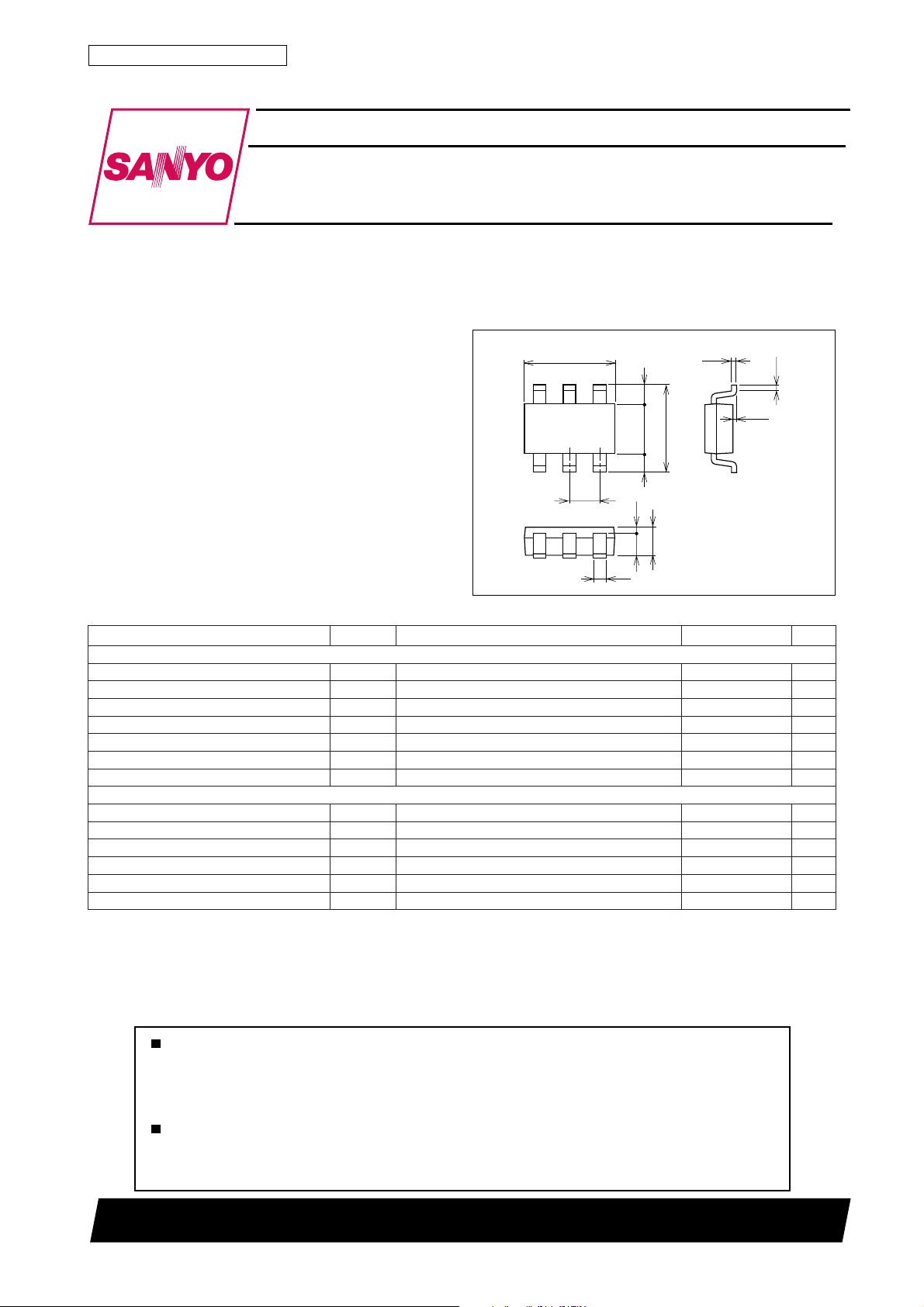
Package Dimensions
unit:mm
2172
4
[CPH6801]
1.6 0.60.6
0.9
0.7 0.2
0.4
2.9
5
6
1
23
0.95
WP ≤ elcycytud,sµ01 ≤ %14–A
elcyc1,evaweniszH05 01A
0.15
0.2
0.05
2.8
1 : Gate
2 : Source
3 : Anode
4 : Drain (Cathode Common)
5 : Drain (Cathode Common)
6 : Drain (Cathode Common)
SANYO : CPH6
02–V
01±V
1–A
9.0W
˚C
˚C
51V
51V
1A
˚C
˚C
31000TS (KOTO) TA-2492 No.6419–1/5
CPH6801
Electrical Characteristics at Ta = 25˚C
retemaraPlobmySsnoitidnoC
]TEFSOM[
egatloVnwodkaerBecruoS-ot-niarDV
tnerruCniarDegatloVetaG-oreZI
tnerruCegakaeLecruoS-ot-etaGI
egatloVffotuCV
ecnattimdArefsnarTdrawroF|sfy|VSDI,V01–=
R
ecnatsiseRetatS-nOecruoS-ot-niarDcitatS
R
ecnaticapaCtupnIssiCV
ecnaticapaCtuptuOssoCV
ecnaticapaCrefsnarTesreveRssrCV
emiTyaleDNO-nruTt
emiTesiRt
emiTyaleDFFO-nruTt
emiTllaFt
egrahCetaGlatoTgQVSDV,V01–=
egrahCecruoS-ot-etaGsgQVSDV,V01–=
egrahC"relliM"niarD-ot-etaGdgQVSDV,V01–=
egatloVdrawroFedoiDV
]DBS[
egatloVesreveRV
egatloVdrawroF
tnerruCesreveRI
ecnaticapaClanimretretnICV
emiTyrevoceResreveRt
ecnatsiseRlamrehTa-jhtR 011
Marking : QB
I
SSD)RB(
D
V
SSD
V
SSG
)ffo(VSDI,V01–=
SG
1)no(IDV,Am005–=
SD
2)no(IDV,Am003–=
SD
)no(d
r
)ffo(d
f
I
DS
S
IRAm1=51V
R
VF1IFA5.0=03.053.0V
VF2IFA1=53.004.0V
VRV6= 005Aµ
R
IFI=
rr
V,Am1–=
0=02–V
SG
V,V02–=
SD
SG
SD
SD
SD
R
R
0=01–Aµ
SG
V,V8±=
0=01±Aµ
SD
Am1–=4.0–4.1–V
D
D
V,A0.1–=
Am005–=0.14.1S
V4–=024055mΩ
SG
V5.2–=036098mΩ
SG
zHM1=f,V01–=001Fp
zHM1=f,V01–=06Fp
zHM1=f,V01–=52Fp
tiucriCtseTdeificepseeS01sn
tiucriCtseTdeificepseeS52sn
tiucriCtseTdeificepseeS72sn
tiucriCtseTdeificepseeS23sn
I,V01–=
SG
I,V01–=
SG
I,V01–=
SG
0=9.0–5.1–V
SG
elcyczHM1=f,V01=24Fp
sgnitaR
nimpytxam
A0.1=5Cn
D
A0.1=1Cn
D
A0.1=1Cn
D
.tiucriCtseTdeificepseeS,Am001= 51sn
tinU
˚C/WMounted on a ceramic board (600mm2×0.8mm)
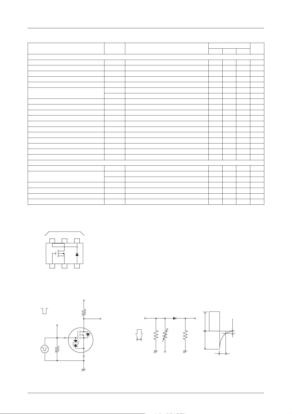
Electrical Connection (Top view)
Cathode Common
D
D
GSA
D
Switching Time Test Circuit trr Test Circuit
[MOSFET] [SBD]
VDD=--10V
V
0V
--4V
PW=10µs
D.C.≤1%
P.G
IN
V
IN
G
50Ω
ID=--500mA
RL=20Ω
D
S
V
OUT
CPH6801
Duty≤10%
50Ω 100Ω 10Ω
10µs
--5V
100mA100mA
10mA
t
rr
No.6419–2/5
 Loading...