


SANYO CPH5702 Datasheet
Any and all SANYO products described or contained herein do not have specifications that can handle
applications that require extremely high levels of reliability, such as life-support systems, aircraft’s
control systems, or other applications whose failure can be reasonably expected to result in serious
physical and/or material damage. Consult with your SANYO representative nearest you before using
any SANYO products described or contained herein in such applications.
SANYO assumes no responsibility for equipment failures that result from using products at values that
exceed, even momentarily, rated values (such as maximum ratings, operating condition ranges,or other
parameters) listed in products specifications of any and all SANYO products described or contained
herein.
TR : NPN Silicon Epitaxial Planar Transistor
SBD : Schottky Barrier Diode
DC/DC Converter Applications
Ordering number:ENN6091
CPH5702
SANYO Electric Co.,Ltd. Semiconductor Company
TOKYO OFFICE Tokyo Bldg., 1-10, 1 Chome, Ueno, Taito-ku, TOKYO, 110-8534 JAPAN
2.9
Features
· Composite type with a NPN transistor and a Schottky
barrier diode contained in one package facilitating
high-density mounting.
· The CPH5702 consists of two chips encapsulated in a
package which are equivalent to the CPH3209 and
the SB07-03C, respectively.
· Ultrasmall-sized package permitting applied sets to
be made small and slim (0.9mm).
Specifications
Absolute Maximum Ratings at Ta = 25˚C
retemaraPlobmySsnoitidnoCsgnitaRtinU
]RT[
egatloVesaB-ot-rotcelloCV
egatloVrettimE-ot-rotcelloCV
egatloVesaB-ot-rettimEV
tnerruCrotcelloCI
)esluP(tnerruCrotcelloCI
tnerruCesaBI
noitapissiDrotcelloCP
erutarepmeTnoitcnuJjT 051
erutarepmeTegarotSgtsT 521+ot55–
]DBS[
egatloVesreveRkaePevititepeRV
egatloVegruSesreveRkaePevititeper-noNV
tnerruCtuptuOegarevAI
tnerruCegruSI
erutarepmeTnoitcnuJjT 521+ot55–
erutarepmeTegarotSgtsT 521+ot55–
OBC
OEC
OBE
C
PC
B
Mounted on a ceramic board (600mm2×0.8mm)
C
MRR
MSR
O
MSF
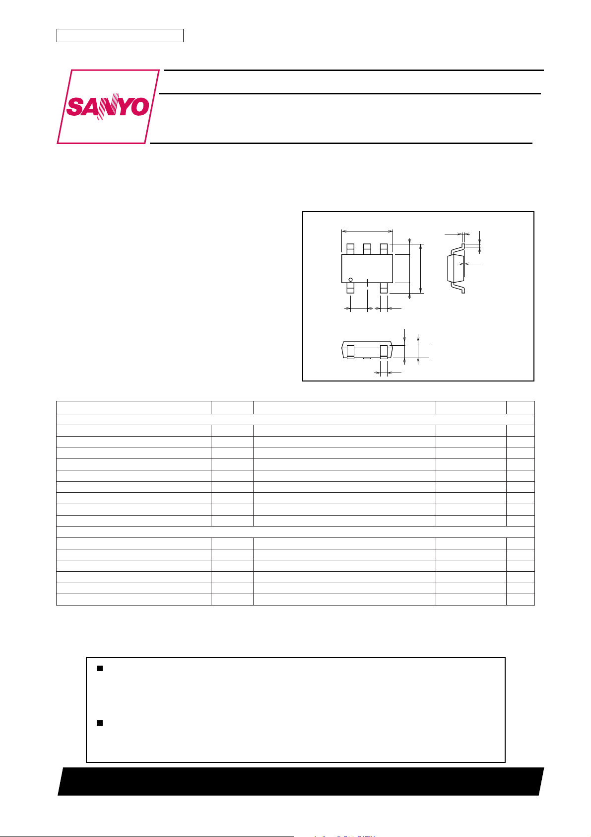
Package Dimensions
unit:mm
2156
[CPH5702]
345
1.6 0.60.6
12
0.40.95
0.2
0.7
0.4
elcyc1,evaweniszH05 5A
0.15
2.8
0.9
0.2
0.05
1 : Cathode
2 : Collector
3 : Base
4 : Emitter
5 : Anode
SANYO : CPH5
04V
03V
5V
3A
5A
006Am
9.0W
˚C
˚C
03V
53V
007Am
˚C
˚C
71299TS (KOTO) TA-1726 No.6091–1/5
Electrical Characteristics at Ta = 25˚C
retemaraPlobmySsnoitidnoC
]RT[
tnerruCffotuCrotcelloCI
tnerruCffotuCrettimEI
niaGtnerruCCD
tcudorPhtdiwdnaB-niaGf
ecnaticapaCtuptuOboCV
egatloVnoitarutaSrettimE-ot-rotcelloC
egatloVnoitarutaSrettimE-ot-esaBV
egatloVnwodkaerBesaB-ot-rotcelloCV
egatloVnwodkaerBrettimE-ot-rotcelloCV
egatloVnwodkaerBesaB-ot-rettimEV
emiTNO-nruTt
emiTegarotSt
emiTFFO-nruTt
]DBS[
egatloVesreveRV
egatloVdrawroFV
tnerruCesreveRI
ecnaticapaClanimretretnICV
emiTyrevoceResreveRt
ecnatsiseRlamrehTa-jhtR 151
V
V
Electrical Connection (Top view)
54
CPH5702
sgnitaR
nimpytxam
V
OBC
V
OBE
h
3
V
EF
V
T
1ICI,A5.1=
)tas(EC
2ICI,A5.1=
)tas(EC
I
)tas(EB
C
I
OBC)RB(
C
I
OEC)RB(
C
I
OBE)RB(
E
no
gts
f
I
R
R
I
F
F
VRV51= 08Aµ
R
R
IFI=
rr
I,V02=
BC
BE
EC
EC
BC
R
0=1.0Aµ
E
I,V4=
0=1.0Aµ
C
I,V2=
Am005=
C
I,V01=
Am005=
C
zHM1=f,V01=
Am03=
B
Am57=
B
I,A5.1=
Am03=38.02.1V
B
I,Aµ01=
0=04V
E
R,Am1=
=∞ 03V
EB
I,Am1=
0=5V
C
Aµ003=03V
Am007= 55.0V
.tiucriCtseTdeificepseeS03sn
.tiucriCtseTdeificepseeS003sn
.tiucriCtseTdeificepseeS51sn
elcyczHM1=f,V01=82Fp
.tiucriCtseTdeificepseeS,Am001= 01sn
002065
054zHM
02Fp
021581Vm
501551Vm
tinU
˚C/WMounted on a ceramic board (600mm2×0.8mm)
1
Switching Time Test Circuit
(TR)
PW=20µs
D.C.≤1%
20I
(For PNP, the polarity is reversed.)
(SBD)
Duty≤10%
INPUT
50Ω
=–20IB2=IC=500mA
B1
VBE=–5V
2
I
B1
I
B2
R
B
V
R
++
100µF 470µF
1 : Cathode
2 : Collector
3 : Base
4 : Emitter
5 : Anode
R
L
VCC=12V
OUTPUT
10µs
50Ω
–5V
100Ω
10Ω
100mA
100mA
10mA
t
rr
No.6091–2/5
 Loading...