

Page 1
Service Manual
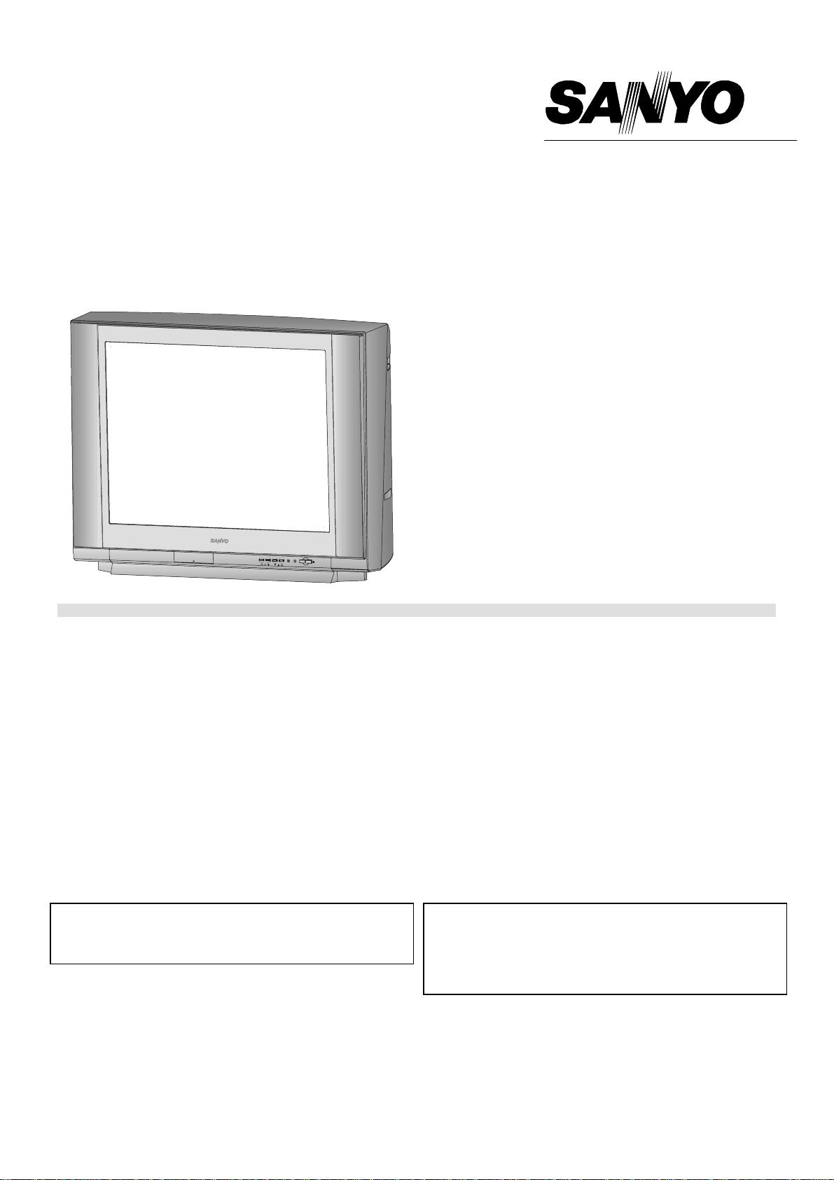
Colour Television True Flat
Indice
1.
Safety instructions..................................................................................................................................1
2.
WARNING.............................................................................................................................................. 1
3.
Precaution against X-Rays...................................................................................................................... 1
4.
Recommendations to protect our environment........................................................................................1
5.
TECHNICAL CHARATERISTICS. .......................................................................................................... 2
6.
Safety..................................................................................................................................................... 2
7.
EMC (Electromagnetic Compati bility) ..................................................................................................... 2
8.
Factory special mode ............................................................................................................................. 2
9.
Automat ic channel search reactiv ating ...................................................................................................3
10. Service Menu......................................................................................................................................... 3
11. CONNECTED DOCUMENTS................................................................................................................. 3
12. MOUNTED CIRCUITS CODES. ............................................................................................................. 3
13. CABINET PARTS LIST .......................................................................................................................... 4
13.1. CABINET PARTS LIST OF CHASSIS CE29FFV2-F........................................................................ 4
13.2. CABINET PARTS LIST OF CE29FFV2-F........................................................................................5
14. PARTS LIST...........................................................................................................................................6
Model:
CE29FFV2-F
CRT 29” Philips A68ERF012X013
CRT 29” Samsung A68QCP993X001
CHASSIS 2114
EB5-C 21"/25" / 28" /29"
Give complete “SERVICE PART No” for parts order or
servi cing, it i s shown on the rating sheet on the cabi net
back of t he TV set.
30-09-2003
Note
This TV receiver will not work properly in foreign
countries where the television transmission system and
power source diff er fr om the design specif icat ions. Refer
to the specifications for the design specifications.
Ref. Nº
MS CE29FFV2-F
Page 2
Serv ice Manual SM CE 29FFV2-F
1. Safety instructions
Read this page befor e doing any operation of adjustm ent, maintenance or repair the TV set described.
Only ski lled personnel of Sanyo Technical Serv ice should do the adjustment, m aintenance or repair of TV set.
2. WARNING
For the corr ect and safe use of the T V set, it is essential that the serv ice personnel follow the process of safety
generally ac c epted and the safety pr ec autions specified in this m anual.
An isolation transformer should be connected in the power line between the receiver and the AC line when a
servi c e is performed on the prim ar y si de of the converter tr ansformer of the set.
The deflection heat si nk is connected to -12V.
3. Precaution against X-Rays
The prim ary source of X-RADIATI ON in the telev ision receiv er is the picture t ube. The picture tube is speciall y
constructed t o li m i t X-RADI AT IO N em i ssions. For conti nued X-RADI ATI ON pr otect i on, t he repl acem ent tube m ust
be the sam e type as the or igi nal i ncl uding suf f i x l ett er. Ex cessive high v ol t age m ay produce pot ent ial l y hazar dous
X-RADIATIO N. T o av oi d such hazards, the high v ol tage m ust be mai ntained wit hin specif i ed lim i t. If hi gh v oltage
exceeds specified limits, take necessary correctiv e action. Follow the instructions carefully for +B1 v olt power
supply adjustment, and high voltage adjustment to maintain the high v oltage within the specifi ed limits.
COMPL IANCE TO STANDARDS
All of those marked with
Replaced with original part s
or must be
WARNING! This TV set contains components which
are particularly sensitive to static electricity (ESD).
It is recommended that all due precaution be taken
handling integrated circuits and semiconductors.
4. Recommendations to protect our environment
Stand-by m ode: In order to sav e energy and to maint ain an optim um picture quali ty, it is advi sable to switch off
the TV using the ON/OFF button located at the front of TV set.
Used batteri es: The batteries in the remote control of these m odels do not contain merc ury. However, SANYO
recommends that you do not dispose of used batteries in domestic refuse. Please, contact your dealer or your
local aut hor ities f or information regardi ng the disposal of used batter ies or your nearest collection point.
Recomm endati on about t he end- of -l i f e: T hese SANY O T V sets hav e been desi gned and m anuf act ured using hi gh
quality materials which can be recycled and reused. In the fut ure, when the life cycle of these sets come to an end,
specialised com panies can disassemble it and reuse cer tain material s. This reduces the impac t of waste in our
environment. Please, contact with your local authori ties for inform ation regarding t he disposal of your set when the
tim e ar r ives. Help us to conserve t he environment we live in!
1
Page 3

Serv ice Manual SM CE 29FFV2-F
5. TECHNICAL CHARATERISTICS.
Cathode-ray tubes
Tuning-system
Reception channels
Reception system
Colour syst em
Program selection
Audio
Speakers
Aerial
Jack for headphones
Clock and alarm Function
Timer Function
AV connectors
Power supply
Consumption
Stereo/Du al Systems
Sound Effects
Auto volume
Clock function
Alarm function
Timer function
TXT
Hotel Mode
Remore ON/OFF
Options by means of Technical Service:
NTSC-M
In-Line, gun Type. Black M atrix. 29” ( 68 c m) True Flat, Invar Plus m ask.
Voltage synthesi s, 100 pr ogr ams in non-volatile memor y , A FT, automatic,
semiautomatic and manual channel-search.
Band I, channel s 2-4 (V HF)=E2-E4
Cable channels S1-S10
Hyperband channels S21-S41
Band III, channels 5-12 (VHF)=E5-E12
Band IV-V, c hannels 21-69 (UHF)=E21-E 69
B/G, D/K, I, L, L' system
PAL, SECAM, (NTSC 4.43, NTSC 3,58) ONLY AV
Sequential sel ec tion fr om the controls on the set. Direct sel ec tion to any program
from the remot e- c ontrol device.
Power-rating 2x8,9 W rms. (10% distortion)
Ω
2 of 8
External aerial sockets 75 Ωs. IEC
Stereo jack 3,5mm. (with independent control)
Switch on and of f of CT V pr ogrammable in real time.
1 Scart connect or 21 pin CENELEC standard AV, RGB and S_Video.
1 Scart connect or 21 pin CENELEC standard AV, RGB
1 RCA Video input (frontal)
2 RCA Audio input (frontal)
220 – 240 VAC 50Hz
83 W ( IEC 107-1)
2,9 W (Stand-by
NICAM and Stereo/Dual (A2)
Pseudo Stereo. Bass boost. Actv. 3D sorround, BBE, spatial stereo
Programmable over 24 hours
Switch on and of f are programmable aver 24 hours.
1,5 Flot and list. 10 Teletext pages memory
It can be programmed in Hotel Mode and Rental Hotel Mode
Tis TV can be switc hed ON/OFF Through the blue scart connec tor.
.
)
6. Safety
It f ulfils the safety requirements established in the regulat ion:
EN 60065:98
7. EMC (Electromagnetic Compatibility)
It f ulfils the EMC requirements established in the regulation:
EN 55013:2001
EN 55020:1994/A11:1996/A13:1999/A14:1999
EN 61000-3-2:1995+A 1:19998+A2:98/A14:2000
EN 61000-3-3:1995
8. Factory special mode
The factory mode i s a special TV working mode intended to hel p in the manufacturing proc ess and it is identified
on the screen with the message “FAC”. This mode is never sui ted for customer use.
The mai n differences respect to norm al mode are:
1- The standby mode is always disabled.
2- The Blue-back (no sync. si gnal present) is disabled.
3- The customer adjustments ( volume, contrast …) work faster.
4- The timer off works but i t does not change to Stand-by mode.
5- Change of programs and TV/AV swithing f aster . Cancelled mute.
In case of finding the TV set in Fact or y mode, it must be taken out of this state. To do so, enter the cloc k setting
menu on the customer OSD and then exit.
2
Page 4

Serv ice Manual SM CE 29FFV2-F
9. Automatic channel search reactivating
In order to reset t he i nit i al aut om ati c c hannel search function, start a channel search i n AUTO m ode f rom the user
tuning m enu and switch-of f t he TV set bef ore any stati on is f ound. The nex t t im e the TV set i s switched on, it will
start an automatic channel - search.
10. Service Menu
The service menu al lows to acces to de relationel parameter s with the TV setting.
The service menu i s accessed by holding down the front k ey ( vol-) and si multaneously pr essing t he teletex t green
key from the remote control. An very detaill explication is in the Service Manual of chassis 2114 (EB5-C).
11. CONNECTED DOCUMENTS.
This Service Manual provides the particul ar information of the model CE 29FFV2-F and it is compl emented with:
1. Serv ice Manual of the CHASIS 2114 (E B 5- C) .
2. Serv ice Electrical schem e of the model CE29FFV1-F .
3. Instruction manual.
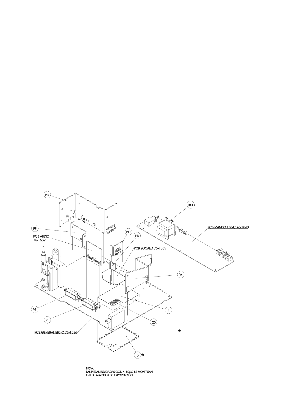
12. MOUNTED CIRCUITS CODES.
CE29FFV2-F
Assy 6110391908 Main + Socket TRC +Audio + Mandos
Subassy 7040004207 Socket TRC PCB
Subassy 7140002135 Audio PCB
Subassy 7200002512 PCB Mandos
A68ERF012X013
CE29FFV2-F
Assy 6110391940 Main + Socket TRC +Audio + Mandos
Subassy 7040005949 Socket TRC PCB
Subassy 7140002135 Audio PCB
Subassy 7200003049 PCB Mandos
A68QCP993X001
Note : T he follo wing abb reviations i ndicate:
PHI
SAM
Excl usi ve parts for
Excl usi ve parts for
CTR PHILIPS
CRT SAMSUNG
3
Page 5
13. CABINET PARTS LIST
13.1. CABINET PART S LIST OF CHASSIS CE29FFV2-F
Ref. No. Part No. Description
YG4 0080113111 COMP. Side I F Shield EB5-C
YG5 0080113202 Copper Side IF Shield EB5-C
YG1800 0200826402 LED Holder
Assy PA (Audio)
IC300 0360517304 TDA 8946 J N 1
YR300 0200226108 Heatsink AUDI O EB5-C 25-28-29
YR301 0970200804 Silicon Grease YG6260
YR302 0010106300 Spring CLIP 56379
Assy PD (Defletion)
IC701 0360517007 LA7846N
Q650 0360306708 S 2055 N
Q750 0360309009 BD242BFP
YR650 0200226009 Heatsink Deflec t ion EB5-C
YR651 0970200804 Silicon Grease YG6260
YR652 0010106300 Spring CLIP 56379
YR653 0010106300 Spring CLIP 56379
YR654 0010110401 Spring CLIP 56363
YR655 0970200804 Silicon Grease YG6260
YR656 0970200804 Silicon Grease YG6260
Assy PB
D851 0360378905 Sc hot t k y F M B-G19L 90V 4ATO220
YR851 0200224905 Heatsink TO-220-F
Localiz. Código Descripción
Assy PF(Power supply)
Q800 0360311302 MOS 2SK2545 600V/6A
YR800 0200225811 Heatsink Power Supply EB5-C
YR801 0010110401 Spring CLIP 56363
Assy PT
S901 0330162702 Scart Connector 21 PIN BLU E
YR901 0200420602 MOUNTING-BRKT F2WV
YR902 0890115603 Selftapping Screws DI N 7981F 2, 9X8
Assy PS
S900 0330162603 Scart Connector 21 PIN BLAC K
YR900 0200420602 MOUNTING-BRKT F2WV
YR903 0890115603 Selftapping Screws DI N 7981F 2, 9X8
Assy PC (Zocket CRT)
IC500 0360514228 TDA 6107JF/N3
YR500 0200224806 Heatsink RGB EB5-A
YR501 0970200804 Silicon Grease YG6260
YR502 0050709104 Washer
YR503 0890121106 Screw M3X6 FE/ZN D I N 7985
Serv ice Manual SM CE 29FFV2-F
4
Page 6
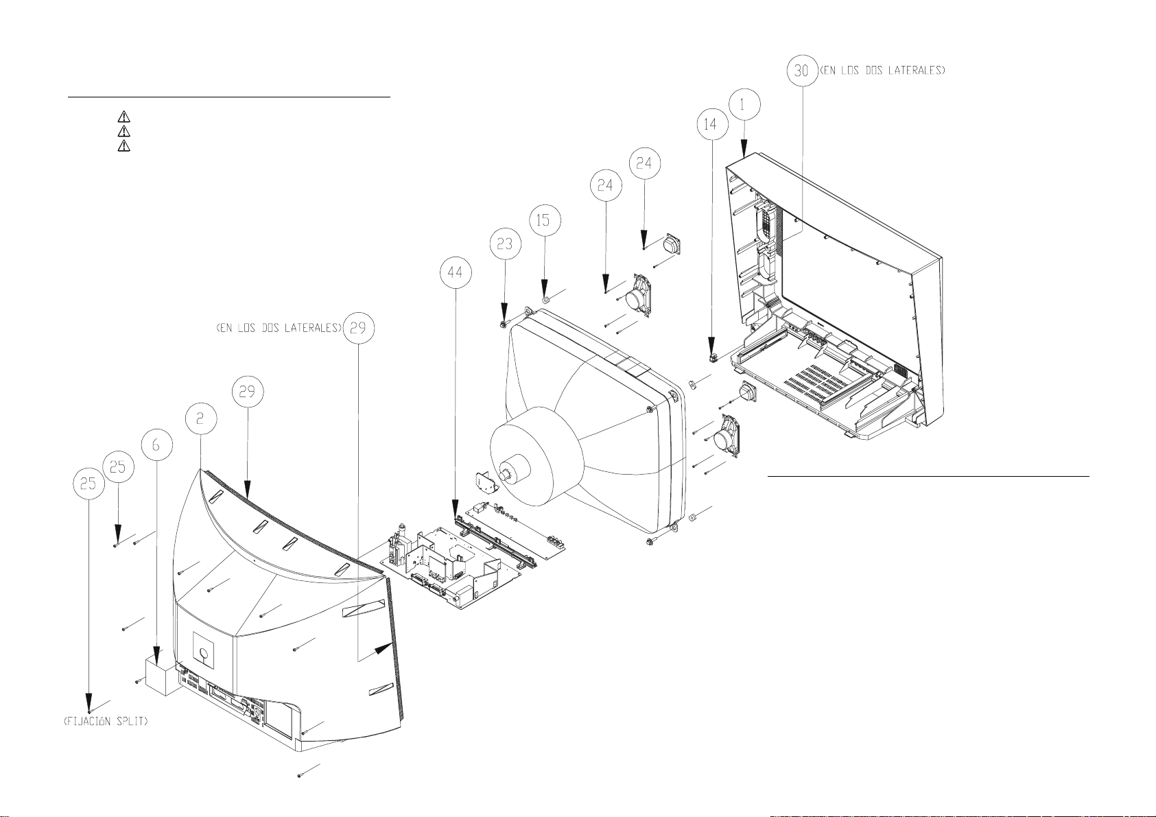
13.2. CABINET PARTS LIST OF CE29FFV2-F
Ref. No. Part. No. Description
YF 1
YF 2
YF 6
YF14 0200819910 AC C ord H older
YF15 0050202316 TRC Cushion 5 mm. (HARDENESS 64)
YF23 0890161508 Screw C L 6, 1X27
YF24 0890191315 Screw AR 4X15
YF25 0890190903 Screw 4X13
YF29 0970141305 Adhesiv e T APE 19 m m . BLACK
YF30 0970136008 Adhesiv e T APE PS
2700054014 Front Cabinet Assy 29" FLAT ATS
0590274809 Back Cov er 29" F LAT
0390258804 Rating Place C E29F F V2-F
"
Serv ice Manual SM CE 29FFV2-F
5
Ref. No. Part. No. Description
(2700054014)
YP 4 0020125225 SAN YO Badge 46, 2X13, 5/SILVER
YP 5 0340208404 T rans .DEC.BOARD 29" F LAT
YP 6 0970304010 R ubber Band 600X2800 M M
YP12 0010111003 Key Spring 21" C2GA
YP13 2130010800 Button Power Assy 29" FLAT
YP13-1 0130216500 Button UNITED BASE 29" FLAT
YP13-2 0130216609 Button Power 29" FLAT
YP14 2130010701 Button Base Assy 29"FLAT
YP14-1 0130216401 Button Unit 29" FLAT
YP14-2 0130216302 Button United BASE 29" FLAT
YP16 0200628410 RAIL Lateral PCB 29" F LAT
YP19 0590275103 Door 29" FLAT
Page 7

Serv ice Manual SM CE 29FFV2-F
Ref. No. Part No. Description Ref. No. Part No. Description
14. PARTS LIST
PCB SOCKET TRC
CONNECTORS
CON_FD 0160220729 Polarized Band 4P 520+6+6
CON_FH 0160230819 Polarized Band Gray 5P. 450+6+ 6
CAPACITORS
C500 0270341324 Poly es t er 100 nF . 10% 250V.
C501 0250322815 Elec t roly t ic 10 µF . 250V.
C503 0240590901 C eram ic 2200 pF + 80-20% 2KV.
DIODES
D500 0360007215 BAV21 DIODE
D501 0360007215 BAV21 DIODE
D502 0360007215 BAV21 DIODE
E500 0640705117 Eyelet 2,5-3
FD1 0330144205 Ribbon Wire Holder 4 P.
FH1 0330144304 Ribbon Wire Holder 5 P.
FK 0640300604 Earth Wire 340 mm .
INTEGRATED CIRCUITS
IC500 0360514228 TDA 6107JF/N3
J117 0470040007 Jumper Lead 0,6 mm.
L502 0090304924 Choke R.F. 470 µH. 10%
L506 PHI 0090208307 Coil 75 µH. 10% 1,5 A. R -7, 5
L506 SAM 0090209305 Coil 59 µH. 10% 1,5 A.
PCB04
RESISTORS
R500 0790741409 Solid 1, 5 KΩ 10% 1/2W.
R501 0790741409 Solid 1, 5 KΩ 10% 1/2W.
R502 0790741409 Solid 1, 5 KΩ 10% 1/2W.
R503 0790741409 Solid 1, 5 KΩ 10% 1/2W.
R504 0790741409 Solid 1, 5 KΩ 10% 1/2W.
R505 0790239008 R . M . G. SMD 1 KΩ T<=5%
R506
R507 0790227003 R . M . G. SMD 100 Ω T<=5%
R508 0790227003 R . M . G. SMD 100 Ω T<=5%
R509 0790227003 R . M . G. SMD 100 Ω T<=5%
R510 0790242002 R . M . G. SMD 1,8 KΩ 5% 1/10W.
R511 0790242002 R . M . G. SMD 1,8 KΩ 5% 1/10W.
R512 0790242002 R . M . G. SMD 1,8 KΩ 5% 1/10W.
ZOCALO
0750153520 Socket PC B 5-C
0790535702 Fuse 10 Ω 5% 0,33W.
0330162108 Socket T R C D iam et er 22, 5 m m .
MAIN PCB
CN_G2 0640706503 BLUE G2 Wire WITH T W O T erm inalS
CN_KV 0330272204 2P. Connector Shield CABLE 400MM
CN_NA 0330193608 4P. Connector
CN_NB 0330198706 10 P. Connect or
CN_NC 0330196601 7P. Connector
RESISTORS
C100 0230600702 C eram ic SM D 100 nF. 10% 25V.
C102 0230600702 C eram ic SM D 100 nF. 10% 25V.
C103 0230360604 C eram ic SM D 1000 pF. 10% 50V.
C104 0250321072 Elec t roly t ic 10 µF . 63V.
C105 0230480808 C eram ic SM D 10 nF. 10% 50V.
C106 0270101322 Poly es t er 1000 pF . 5% 400V.
C107 0230480808 C eram ic SM D 10 nF. 10% 50V.
C108 0230180309 C eram ic SM D 33 pF. 1% 50V.
C109 0230180309 C eram ic SM D 33 pF. 1% 50V.
C112 0230600801 C eram ic SM D 100 nF. +80-20% 25V.
C113 0230360604 C eram ic SM D 1000 pF. 10% 50V.
C114 0230360604 C eram ic SM D 1000 pF. 10% 50V.
C115 0230360604 Ceramic SMD 1000 pF. 10% 50V.
C116 0230360604 Ceramic SMD 1000 pF. 10% 50V.
C118 0230360604 C eram ic SM D 1000 pF. 10% 50V.
C120 0230480808 C eram ic SM D 10 nF. 10% 50V.
C190 0230600702 C eram ic SM D 100 nF. 10% 25V.
C191 0230640401 C eram ic SM D 220 nF. 10% 16V.
C200 0250321072 Elec t roly t ic 10 µF . 63V.
C201 0230360604 C eram ic SM D 1000 pF. 10% 50V.
C202 0230360604 C eram ic SM D 1000 pF. 10% 50V.
C203 0230600702 C eram ic SM D 100 nF. 10% 25V.
C204 0230600702 C eram ic SM D 100 nF. 10% 25V.
C207 0250321072 Elec t roly t ic 10 µF . 63V.
C209 0230480808 C eram ic SM D 10 nF. 10% 50V.
C210 0230600801 C eram ic SM D 100 nF. +80-20% 25V.
C250 0230600801 C eram ic SM D 100 nF. +80-20% 25V.
C251 0250461217 Elec t roly t ic 100 µF . 25V.
C252 0270341480 Poly es t er 100 nF . 10% 63V.
C256 0230480808 C eram ic SM D 10 nF. 10% 50V.
C257 0270341480 Poly es t er 100 nF . 10% 63V.
C258 0230480808 C eram ic SM D 10 nF. 10% 50V.
C259 0230600801 C eram ic SM D 100 nF. +80-20% 25V.
C260 0250410859 Elec t roly t ic 47 µF . 25V.
C261 0230600801 C eram ic SM D 100 nF. +80-20% 25V.
C300 0250572310 Elec t roly t ic 1000 µF . 25V.
C301 0230600702 C eram ic SM D 100 nF. 10% 25V.
C302 0230360604 C eram ic SM D 1000 pF. 10% 50V.
C303 0230360604 C eram ic SM D 1000 pF. 10% 50V.
C304 0230640401 C eram ic SM D 220 nF. 10% 16V.
C305 0230640401 C eram ic SM D 220 nF. 10% 16V.
C306 0230640401 C eram ic SM D 220 nF. 10% 16V.
C307 0230640401 C eram ic SM D 220 nF. 10% 16V.
C308 0250321072 Elec t roly t ic 10 µF . 63V.
C309 0250321072 Elec t roly t ic 10 µF . 63V.
C310 0240551309 C eram ic 1000 pF . 10% 50V.
C311 0270341324 Poly es t er 100 nF . 10% 250V.
C312 0270341324 Poly es t er 100 nF . 10% 250V.
C352 0250410859 Elec t roly t ic 47 µF . 25V.
C353 0250410859 Elec t roly t ic 47 µF . 25V.
C354 0230600801 C eram ic SM D 100 nF. +80-20% 25V.
C355 0230600801 C eram ic SM D 100 nF. +80-20% 25V.
C356 0250500618 Elec t roly t ic 220 µF . 16V.
C357 0250461217 Elec t roly t ic 100 µF . 25V.
C359 0230480808 C eram ic SM D 10 nF. 10% 50V.
C361 0250461217 Elec t roly t ic 100 µF . 25V.
C362 0230160400 Ceramic SMD 22 pF. 1% 50V.
C363 0230160400 Ceramic SMD 22 pF. 1% 50V.
C364 0230240400 Ceramic SMD 100 pF. 5% 50V.
C365 0230240400 Ceramic SMD 100 pF. 5% 50V.
C400 0250461217 Elec t roly t ic 100 µF. 25V.
C401 0230600801 C eram ic SM D 100 nF. +80-20% 25V.
C402 0230740003 C eram ic SM D 2,2 µF. 10V. +80-20%
C403 0230520504 C eram ic SM D 22 nF. 10% 50V.
C404 0230640401 C eram ic SM D 220 nF. 10% 16V.
C405 0230360604 C eram ic SM D 1000 pF. 10% 50V.
C406 0230600702 C eram ic SM D 100 nF. 10% 25V.
C407 0230740003 C eram ic SM D 2,2 µF. 10V. +80-20%
C408 0230600702 C eram ic SM D 100 nF. 10% 25V.
C409 0230600702 C eram ic SM D 100 nF. 10% 25V.
C410 0230600702 C eram ic SM D 100 nF. 10% 25V.
C411 0230180309 C eram ic SM D 33 pF. 1% 50V.
C412 0230180309 C eram ic SM D 33 pF. 1% 50V.
C413 0230740003 C eram ic SM D 2,2 µF. 10V. +80-20%
C414 0230520504 C eram ic SM D 22 nF. 10% 50V.
C415 0250461217 Elec t roly t ic 100 µF. 25V.
C416 0230520504 C eram ic SM D 22 nF. 10% 50V.
C417 0230400202 C eram ic SM D 2200 pF. 10% 50V.
C418 0230240400 Ceramic SMD 100 pF. 5% 50V.
C419 0230200503 Ceramic SMD 47 pF. 5% 50V.
C420 0230680308 C eram ic SM D 470 nF. 10% 16V.
C421 0230440406 C eram ic SM D 4700 pF. 10% 50V.
C422 0230240400 Ceramic SMD 100 pF. 5% 50V.
C423 0230360604 Ceramic SMD 1000 pF. 10% 50V.
C424 0230600702 Ceramic SMD 100 nF. 10% 25V.
C425 0260340906 Poly propy lene 100 nF . 5% 100V.
C426 0230360604 Ceramic SMD 1000 pF. 10% 50V.
C427 0230600702 C eram ic SM D 100 nF. 10% 25V.
6
Page 8

Serv ice Manual SM CE 29FFV2-F
Ref. No. Part No. Description Ref. No. Part No. Description
C428 0230240400 Ceramic SMD 100 pF. 5% 50V.
C429 0230240400 C eram ic SM D 100 pF. 5% 50V.
C430 0230240400 C eram ic SM D 100 pF. 5% 50V.
C431 0230240400 C eram ic SM D 100 pF. 5% 50V.
C432 0230360604 C eram ic SM D 1000 pF. 10% 50V.
C433 0230240400 C eram ic SM D 100 pF. 5% 50V.
C434 0230680308 C eram ic SM D 470 nF. 10% 16V.
C435 0250280856 Elec t roly t ic 4, 7 µF . 100V.
C436 0230600801 C eram ic SM D 100 nF. +80-20% 25V.
C437 0230360604 Ceramic SMD 1000 pF. 10% 50V.
C438 0230360604 C eram ic SM D 1000 pF. 10% 50V.
C439 0230480808 Ceramic SMD 10 nF. 10% 50V.
C442 0250321072 Elec t roly t ic 10 µF . 63V.
C443 0230440406 C eram ic SM D 4700 pF. 10% 50V.
C450 0230240400 Ceramic SMD 100 pF. 5% 50V.
C451 0230240400 Ceramic SMD 100 pF. 5% 50V.
C452 0230240400 Ceramic SMD 100 pF. 5% 50V.
C453 0230520504 C eram ic SM D 22 nF. 10% 50V.
C454 0230520504 C eram ic SM D 22 nF. 10% 50V.
C455 0230520504 C eram ic SM D 22 nF. 10% 50V.
C600A 0270341324 Polyester 100 nF. 10% 250V.
C601 0270140122 Poly es t er 2200 pF . 10% 400V.
C603 0230520504 C eram ic SM D 22 nF. 10% 50V.
C604 0230720203 C eram ic SM D 1 µF. 16V. +80-20%
C650B 0260260500 Polypropylene 22 nF. 3,5% 630V
C651
C652A PHI 0260400908 Poly propy lene 330 nF . 5% 250V.
C652B SAM 0260393004 Polypropylene 300 nF. 5% 250V.
C653
C654A PHI 0260140504 Poly propy lene 2200 pF . 3, 5% 1,6 KV.
C654B SAM 0260123500 Polypropylene 1500 pF. 3, 5% 1600V
C655A PHI 0270290802 Poly es t er 39 nF . 5% 400V.
C655A SAM 0270281231 Polyester 33 nF . 10% 400V.
C656 0250115318 Elec t roly t ic 2, 2 µF. 160V. 6,3X11
C657 0240132035 C eram ic 470 pF . 10% 1KV.
C658 0230260705 C eram ic SM D 150 pF. 10% 630V. 1206
C659A 0250504107 Electrolytic 220 µF. 200V. 18x 35, 5
C660 0230340408 C eram ic SM D 680 pF. 10% 630V. 1206
C661 0250283835 Elec t roly t ic 4, 7 µF . 250V.
C663 0230600702 C eram ic SM D 100 nF. 10% 25V.
C668 0250283835 Elec t roly t ic 4, 7 µF . 250V.
C669 0230340408 C eram ic SM D 680 pF. 10% 630V. 1206
C670 0270341324 Poly es t er 100 nF . 10% 250V.
C674 0230520504 C eram ic SM D 22 nF. 10% 50V.
C675 0230600702 C eram ic SM D 100 nF. 10% 25V.
C680 0250220472 Elec t roly t ic 1 µF . 100V.
C700 0250463718 Elec t roly t ic 100 µF . 50V. 8X11,5
C701 0250463718 Elec t roly t ic 100 µF . 50V. 8X11,5
C703 0270370588 Poly es t er 180 nF . 10% 63V.
C704 0250463718 Elec t roly t ic 100 µF . 50V. 8X11,5
C710 0270341480 Poly es t er 100 nF . 10% 63V.
C711 0230360604 Ceramic SMD 1000 pF. 10% 50V.
C712 0270220726 Poly es t er 10 nF . 10% 250V.
C750 0230360604 C eram ic SM D 1000 pF. 10% 50V.
C751 0230480808 Ceramic SMD 10 nF. 10% 50V.
C753 0250284023 Elec t roly t ic 4, 7 µF . 160V.
C802 0240134767 C eram ic 1000 pF . + -20% 1KV.
C803 0240134767 C eram ic 1000 pF . + -20% 1KV.
C806 0230240400 C eram ic SM D 100 pF. 5% 50V.
C807 0230200503 C eram ic SM D 47 pF. 5% 50V.
C809 0230300709 C eram ic SM D 330 pF. 5% 50V.
C810 0250503661 Elec t roly t ic . 220 µF. 385V. 30X35
C811 0250412970 Elec t roly t ic 47 µF . 50V.
C812
C813 0230360505 C eram ic SM D 1000 pF 5% 100V.0805
C814 0230260309 C eram ic SM D 150 pF. 10% 1KV. 1206
C816
C817 0230300303 C eram ic SM D 330 pF. 10% 630V. 1206
C818 0230300303 C eram ic SM D 330 pF. 10% 630V. 1206
C850 0230280505 C eram ic SM D 220 pF. 10% 1KV. 1206
C851 0230360604 C eram ic SM D 1000 pF. 10% 50V.
C852 0230360604 C eram ic SM D 1000 pF. 10% 50V.
C855 0230600801 C eram ic SM D 100 nF. +80-20% 25V.
C856 0250465218 Elec t roly t ic 100 µF . 200V.
C857 0250601515 Elec t roly t ic 2200 µF . 25V. R-7,5
C858 0250531910 Elec t roly t ic 470µF . 25V. 10X12,5
0260223003 Polypropylene 15 nF . 3, 5% 1600V.
0260433065 Polypropylene 820nF . 5% 250V
0240136135 Ceramic Capacitor 1000 pF. 20% 4KV.
0240136135 Ceramic Capacitor 1000 pF. 20% 4KV.
C859 0250531910 Elec t roly t ic 470µF . 25V. 10X12,5
C860 0250572419 Elec t roly t ic 1000 µF . 16V.
C861 0250572419 Elec t roly t ic 1000 µF . 16V.
C862 0230640401 C eram ic SM D 220 nF. 10% 16V.
C863 0230360604 C eram ic SM D 1000 pF. 10% 50V.
C866 0230360604 C eram ic SM D 1000 pF. 10% 50V.
C868 0250321072 Elec t roly t ic 10 µF . 63V.
C870 0250321072 Elec t roly t ic 10 µF . 63V.
C871 0230360604 Ceramic SMD 1000 pF. 10% 50V.
C874 0250461217 Elec t roly t ic 100 µF . 25V.
C875 0230400202 C eram ic SM D 2200 pF. 10% 50V.
C876 0230360604 C eram ic SM D 1000 pF. 10% 50V.
C900 0230320608 Ceramic SMD 470 pF. 5% 50V.
C901 0230320608 Ceramic SMD 470 pF. 5% 50V.
C902 0230320608 Ceramic SMD 470 pF. 5% 50V.
C903 0230320608 Ceramic SMD 470 pF. 5% 50V.
C904 0230320608 Ceramic SMD 470 pF. 5% 50V.
C905 0230320608 Ceramic SMD 470 pF. 5% 50V.
C906 0230320608 Ceramic SMD 470 pF. 5% 50V.
C907 0250321072 Elec t roly t ic 10 µF . 63V.
C913 0230240400 Ceramic SMD 100 pF. 5% 50V.
C914 0230240400 Ceramic SMD 100 pF. 5% 50V.
C917 0230240400 Ceramic SMD 100 pF. 5% 50V.
C918 0230600801 C eram ic SM D 100 nF. +80-20% 25V.
C920 0250321072 Elec t roly t ic 10 µF . 63V.
C921 0250321072 Elec t roly t ic 10 µF . 63V.
C923 0250321072 Elec t roly t ic 10 µF . 63V.
C925 0230320608 Ceramic SMD 470 pF. 5% 50V.
C926 0250410859 Elec t roly t ic 47 µF . 25V.
C928 0250410859 Elec t roly t ic 47 µF . 25V.
C930 0250410859 Elec t roly t ic 47 µF . 25V.
C931 0250410859 Elec t roly t ic 47 µF . 25V.
C934 0250410859 Elec t roly t ic 47 µF . 25V.
C935 0250410859 Elec t roly t ic 47 µF . 25V.
C936 0250410859 Elec t roly t ic 47 µF . 25V.
C938 0250321072 Elec t roly t ic 10 µF . 63V.
C939 0230720203 C eram ic SM D 1 µF. 16V. +80-20%
C940 0230720203 C eram ic SM D 1 µF. 16V. +80-20%
DIODE
D102 0360601512 SM D LS4148
D105 0360130819 1N 4148
D106 0360601512 SM D LS4148
D107 0360130819 1N 4148
D108 0360102602 Zener BZX79C3V3
D190 0360130819 1N 4148
D200 0360601512 SM D LS4148
D201 0360601512 SM D LS4148
D250 0360706014 HZT33-02 RE
D251 0360601512 SM D LS4148
D300 0360103204 Zener BZX79C5V1
D301 0360103204 Zener BZX79C5V1
D350 0360601512 SM D LS4148
D351 0360601512 SM D LS4148
D401 0360602411 Z ener SM D BZ T 55C 6V2
D402 0360601512 SM D LS4148
D600 0360605604 SM D BAV103 200V 0, 25A
D650 0360118608 ERD07-15L
D651 0360007215 BAV21 DIODE
D652A 0360380109 RU3AM
D653 0360377006 ERB44-04
D654 0360601512 SM D LS4148
D655 0360603914 Z ener SM D BZ T 55C 33
D658 0360601512 SM D LS4148
D659 0360130819 1N 4148
D660 0360601512 SM D LS4148
D661 0360603914 Z ener SM D BZ T 55C 33
D663 0360377006 ERB44-04
D672 0360601512 SM D LS4148
D674 0360603310 Z ener SM D BZ T 55C 15
D675 0360601512 SM D LS4148
D683 0360601512 SM D LS4148
D700 0360601512 SM D LS4148
D701 0360130629 1N 4007 R L
D702 0360130819 1N 4148
D703 0360603914 Z ener SM D BZ T 55C 33
7
Page 9

Serv ice Manual SM CE 29FFV2-F
Ref. No. Part No. Description Ref. No. Part No. Description
D704 0360130819 1N 4148
D705 0360135107 Zener BZX79C8V2
D750 0360601512 SM D LS4148
D751 0360105100 Zener BZX79C11
D752 0360130819 1N 4148
D753 0360130819 1N 4148
D754 0360607006 Z ener SM D M M SZ 56T1
D800 PHI 0360372411 ERC05-10B V1
D800 SAM 0360379705 1R5NH41 1000V 1.5A
D801 PHI 0360372411 ERC05-10B V1
D801 SAM 0360379705 1R5NH41 1000V 1.5A
D802 PHI 0360372411 ERC05-10B V1
D802 SAM 0360379705 1R5NH41 1000V 1.5A
D803 PHI 0360372411 ERC05-10B V1
D803 SAM 0360379705 1R5NH41 1000V 1.5A
D804 0360602411 Z ener SM D BZ T 55C 6V2
D806 0360376909 ERB44-02
D850 0360374409 RU4B LF-T3
D851 0360378905 Sc hot t k y F M B-G19L 90V 4ATO220
D852A 0360379606 1R5GH45 400V 1.5A
D853A 0360379606 1R5GH45 400V 1.5A
D854 0360376909 ERB44-02
D855A 0360376701 Schottky RK 19 V1 90V 1, 5A
D857 0360606115 Z ener SM D BZ T 55C 4V3
D859 0360606115 Z ener SM D BZ T 55C 4V3
D860 0360602213 Z ener SM D BZ T 55C 5V1
D861 0360603914 Z ener SM D BZ T 55C 33
D862 0360130819 1N 4148
D863 0360104202 Zener BZX79C6V2
D866 0360601512 SM D LS4148
D867 0360130819 1N 4148
D870 0360130819 1N 4148
D871 0360130819 1N 4148
D900 0360602213 Z ener SM D BZ T 55C 5V1
D901 0360602213 Z ener SM D BZ T 55C 5V1
D902 0360602213 Z ener SM D BZ T 55C 5V1
D903 0360602213 Z ener SM D BZ T 55C 5V1
D904 0360602213 Z ener SM D BZ T 55C 5V1
D905 0360602213 Z ener SM D BZ T 55C 5V1
D906 0360602213 Z ener SM D BZ T 55C 5V1
D908 0360602213 Z ener SM D BZ T 55C 5V1
D909 0360602213 Z ener SM D BZ T 55C 5V1
D910 0360602213 Z ener SM D BZ T 55C 5V1
D911 0360602213 Z ener SM D BZ T 55C 5V1
D912 0360602213 Z ener SM D BZ T 55C 5V1
D914 0360602213 Z ener SM D BZ T 55C 5V1
D917 0360602213 Z ener SM D BZ T 55C 5V1
D918 0360601512 SM D LS4148
D919 0360601512 SM D LS4148
D920 0360601512 SM D LS4148
D921 0360130819 1N 4148
CONNECTORS
FA 0330271305 2P. Socket W / C LIP
FB1 0330191701 2P. Socket
FB2 0330270109 2 P. Socket
FD 0330144205 Ribbon Wire Holder 4 P.
FF1 0330190000 2P. Connector
FF2 0330270109 2 P. Soc k et
FH 0330144304 Ribbon Wire Holder 5 P.
INTEGRATED CIRCUITS
IC100 0360519003 SAA 5564PS
IC125 0360712012 SMD M24C08-WMN6T
IC300 0360517304 TDA 8946 J N 1
IC350 0360472609 KA2209B
IC400 0360516900 TDA 8874PS N 1
IC701 0360517007 LA7846N
IC800 0360517205 MC44603ADW SMD
IC801
IC850 0360378764 KA431LZTA TO-92
IC852 0360473409 LD1117V33C TO220
IC853 0360472708 KA78R08TU
IC854 0360472807 KA78R05-STU
IC900 0360708804 LA 7221
0360491203 OPTO TCET1101G
JUMPERS
JO104 0790701106 R . M . G. SM D 0 Ω 1/10W.
JO1050 0790701106 R.M. G. SM D 0 Ω 1/10W.
JO1051 0790701106 R.M. G. SM D 0 Ω 1/10W.
JO1052 0790701106 R.M. G. SM D 0 Ω 1/10W.
JO202 0790701106 R . M . G. SM D 0 Ω 1/10W.
JO252 0790701106 R . M . G. SM D 0 Ω 1/10W.
JO253 0790701106 R . M . G. SM D 0 Ω 1/10W.
JO701 0790701106 R.M.G. SMD 0 Ω 1/10W.
JO702 0790701106 R.M.G. SMD 0 Ω 1/10W.
J129 0790701106 R.M.G. SM D 0 Ω 1/10W.
J159 0790126700 Carbon 100 Ω 5% 1/6W.
J198 0790701106 R.M.G. SM D 0 Ω 1/10W.
J235 0790701106 R.M.G. SM D 0 Ω 1/10W.
J236 0790701106 R.M.G. SM D 0 Ω 1/10W.
J237 0790701106 R.M.G. SM D 0 Ω 1/10W.
J242 0790701106 R.M.G. SM D 0 Ω 1/10W.
J248 0790701106 R.M.G. SM D 0 Ω 1/10W.
J250 0790701106 R.M.G. SM D 0 Ω 1/10W.
J251 0790701106 R.M.G. SM D 0 Ω 1/10W.
J255 0790701106 R.M.G. SM D 0 Ω 1/10W.
J256 0790701106 R.M.G. SM D 0 Ω 1/10W.
J264 0790701106 R.M.G. SM D 0 Ω 1/10W.
J267 0790701106 R.M.G. SM D 0 Ω 1/10W.
KVBM 0330191701 2P. Socket
K300 0330330002 8P. Connector
K301 0330330002 8P. Connector
K302 0330490301 Connector Assy 10P W/WireS 260 MM
COILS
L100 0090305327 Peaking C oil 10 µH . 10%
L101 0620005801 Ferrit e SM D 0805 1K/ 100M H z 0,2A
L102 0620005801 Ferrit e SM D 0805 1K/ 100M H z 0,2A
L104 0620005801 Ferrit e SM D 0805 1K/ 100M H z 0,2A
L250 0090305665 Peaking C oil 4, 7 µH 10% I MAX= 930M A
L251 0090317157 Peaking C oil 0, 39 µH . 10% RADI AL
L252 0090319229 Peaking C oil 4, 7 µH . 10%
L300 0090817305 Axial I nduc t or 12 µH . 10% 1,8A.
L301 0620005900 F errit e SM D 1206 600 Ω/100MH 1,5A
L302 0620005900 F errit e SM D 1206 600 Ω/100MH 1,5A
L303 0620005900 F errit e SM D 1206 600 Ω/100MH 1,5A
L304 0620005900 F errit e SM D 1206 600 Ω/100MH 1,5A
L305 0090817305 Axial I nduc t or 12 µH . 10% 1,8A.
L350 0470040007 J um per Lead 0, 6 mm.
L351 0470040007 J um per Lead 0, 6 mm.
L400 0090319229 Peaking C oil 4, 7 µH . 10%
L401 0470040007 Jum per Lead 0, 6 mm.
L404 0620011502 F errit e SM D 0603 600 Ω/100MHz
L405 0090319229 Peaking C oil 4, 7 µH . 10%
L410 0470040007 Jum per Lead 0, 6 mm.
L600 0090817206 Axial I nduc t or 3, 3 µH . 10% 2,6A.
L651A 0090804105 Coil 1,3 MH . + -10% 2A. CU 20
L652 0090209115 Fix ed Linealit y C oil
L654 0090817305 Axial I nduc t or 12 µH . 10% 1,8A.
L656 0090207200 Coil 3, 3 M H . 10% 0,175 A.
L661 0620005900 F errit e SM D 1206 600 Ω/100MH 1,5A
L668 0620005900 F errit e SM D 1206 600 Ω/100MH 1,5A
L700 0090305327 Peaking C oil 10 µH . 10%
L703 0090305327 Peaking C oil 10 µH . 10%
L750A 0090502907 E/W Correc t ion C oil 5, 5M H . 14X15
L802 0620005702 F errit e Bead 3, 180 Ω/100MHz
L803 0790109300 Carbon 3,3 Ω 5% 1/4W.
L850 0620005116 Pipe Core 3, 5X4, 5
L851 0620005116 Pipe Core 3, 5X4, 5
L852 0620005116 Pipe Core 3, 5X4, 5
L853 0620005116 Pipe Core 3, 5X4, 5
L854 0620005116 Pipe Core 3, 5X4, 5
L855 0620005116 Pipe Core 3, 5X4, 5
L856 0620005702 Ferrit e Bead 3, 180 Ω/100MHz
L857 0620005900 Ferrit e SM D 1206 600 Ω/100MH 1,5A
L858 0620005900 Ferrit e SM D 1206 600 Ω/100MH 1,5A
L859 0620005900 Ferrit e SM D 1206 600 Ω/100MH 1,5A
L860 0620005900 Ferrit e SM D 1206 600 Ω/100MH 1,5A
L861 0620005702 Ferrit e Bead 3, 180 Ω/100MHz
8
Page 10

Serv ice Manual SM CE 29FFV2-F
Ref. No. Part No. Description Ref. No. Part No. Description
L862 0620005900 Ferrit e SM D 1206 600 Ω/100MH 1,5A
L863 0620005900 Ferrit e SM D 1206 600 Ω/100MH 1,5A
L864 0090817305 Axial I nduc t or 12 µH . 10% 1,8A.
L865 0090817305 Axial I nduc t or 12 µH . 10% 1,8A.
L866 0090319765 Peaking C oil 22 µH . 10% I MAX= 130M A
L900 0470040007 J um per Lead 0, 6 m m .
L901 0470040007 J um per Lead 0, 6 m m .
L902 0470040007 J um per Lead 0, 6 m m .
L903 0090319229 Peaking C oil 4, 7 µH . 10%
L905 0620011502 F errit e SM D 0603 600 Ω/100MHz
PCB11
TRANSISTORS
Q100 0360320501 BRT SMD PD T A124ET
Q101 0360320501 BRT SMD PD T A124ET
Q102 0360320303 SMD BC 847 B
Q104 0360320303 SMD BC 847 B
Q105 0360320303 SMD BC 847 B
Q106 0360320600 BRT SMD PD T C 124ET
Q107 0360321301 SMD BC 857 B
Q190 0360320303 SMD BC 847 B
Q200 0360320303 SMD BC 847 B
Q201 0360320600 BRT SMD PD T C 124ET
Q202 0360321301 SMD BC 857 B
Q203 0360320303 SMD BC 847 B
Q204 0360320303 SMD BC 847 B
Q207 0360320600 BRT SMD PD T C 124ET
Q250 0360320303 SMD BC 847 B
Q251 0360308803 SMD PMBT 2369
Q252 0360320501 BRT SMD PD T A124ET
Q253 0360320501 BRT SMD PD T A124ET
Q254 0360320501 BRT SMD PD T A124ET
Q255 0360320410 SMD BF 570
Q257 0360320600 BRT SMD PD T C 124ET
Q300 0360320600 BRT SMD PD T C 124ET
Q301 0360320600 BRT SMD PD T C 124ET
Q350 0360320600 BRT SMD PD T C 124ET
Q351 0360320600 BRT SMD PD T C 124ET
Q352 0360320600 BRT SMD PD T C 124ET
Q400 0360320303 SMD BC 847 B
Q401 0360320303 SMD BC 847 B
Q600 0360309108 2SC2271D-CTV-AE
Q604 0360321301 SMD BC 857 B
Q650 0360306708 S 2055 N
Q651 0360320303 SMD BC 847 B
Q652 0360320303 SMD BC 847 B
Q653 0360308605 KSP 92 TO-92
Q672 0360308506 KSP 42 TO-92
Q673 0360320303 SMD BC 847 B
Q674 0360321301 SMD BC 857 B
Q750 0360309009 BD242BFP
Q751 0360320600 BRT SMD PD T C 124ET
Q752 0360308605 KSP 92 TO-92
Q753 0360308605 KSP 92 TO-92
Q754 0360308506 KSP 42 TO-92
Q800 0360311302 MOS 2SK2545 600V/6A
Q850 0360311203 MOS 2SK2964 30V/2A SMD
Q851 0360320600 BRT SMD PD T C124ET
Q852 0360311203 MOS 2SK2964 30V/2A SMD
Q853 0360320303 SMD BC 847 B
Q854 0360320303 SMD BC 847 B
Q855 0360320303 SMD BC 847 B
Q856 0360320303 SMD BC 847 B
Q857 0360320600 BRT SMD PD T C124ET
Q858 0360320501 BRT SMD PD T A124ET
Q859 0360320303 SMD BC 847 B
Q861 0360320600 BRT SMD PD T C124ET
Q862 0360308605 KSP 92 TO-92
Q863 0360308506 KSP 42 TO-92
Q900 0360320303 SMD BC 847 B
Q901 0360320303 SMD BC 847 B
Q904 0360308803 SMD PMBT 2369
Q905 0360308803 SMD PMBT 2369
Q906 0360308803 SMD PMBT 2369
Q907 0360321301 SMD BC 857 B
0750153629 MAIN PC B EB5-C
Q908 0360320303 SMD BC 847 B
RESISTORS
R100 0790239008 R . M . G. SMD 1 KΩ T<=5%
R101 0790239008 R . M . G. SMD 1 KΩ T<=5%
R102 0790239008 R . M . G. SMD 1 KΩ T<=5%
R103 0790239008 R . M . G. SMD 1 KΩ T<=5%
R105 0790580203 M et al F ilm 22 KΩ 1% 0,4W.
R106 0790138804 C arbon 1 KΩ 5% 1/6W.
R107 0790138804 C arbon 1 KΩ 5% 1/6W.
R108 0790239008 R . M . G. SMD 1 KΩ T<=5%
R109 0790239008 R . M . G. SMD 1 KΩ T<=5%
R110 0790138804 C arbon 1 KΩ 5% 1/6W.
R112 0790141600 C arbon 1, 5 KΩ 5% 1/6W.
R113 0790146401 C arbon 3, 9 KΩ 5% 1/6W.
R114 0790756001 R . M . G. SMD 24 KΩ 1% 1/8W.
R118 0790239008 R . M . G. SMD 1 KΩ T<=5%
R119 0790239008 R . M . G. SMD 1 KΩ T<=5%
R120 0470040007 J um per Lead 0, 6 mm.
R121 0470040007 J um per Lead 0, 6 mm.
R122 0790237002 R . M . G. SMD 680 Ω T<=5%
R123 0790239008 R . M . G. SMD 1 KΩ T<=5%
R125 0790723506 R . M . G. SMD 47 Ω 1% 1/10W.
R126 0790723506 R . M . G. SMD 47 Ω 1% 1/10W.
R127 0790723506 R . M . G. SMD 47 Ω 1% 1/10W.
R128 0790247001 R . M . G. SMD 4,7 KΩ T<=5%
R129 0790155600 C arbon 22 KΩ 5% 1/6W.
R130 0790741805 R . M . G. SMD 1,5 KΩ T<=5%
R131 0790755706 R . M . G. SMD 23,7 KΩ 1% 1/8W.
R132 0790758304 R . M . G. SMD 39 KΩ 1% 1/8W.
R133 0790255004 R . M . G. SMD 22 KΩ T<=5%
R134 0790255004 R . M . G. SMD 22 KΩ T<=5%
R135 0790239008 R . M . G. SMD 1 KΩ T<=5%
R136 0790138804 C arbon 1 KΩ 5% 1/6W.
R137 0790138804 C arbon 1 KΩ 5% 1/6W.
R138 0790138804 C arbon 1 KΩ 5% 1/6W.
R140 0790239008 R . M . G. SMD 1 KΩ T<=5%
R141 0790126700 Carbon 100 Ω 5% 1/6W.
R142 0790126700 Carbon 100 Ω 5% 1/6W.
R143 0790247001 R . M . G. SMD 4,7 KΩ T<=5%
R144 0790247001 R . M . G. SMD 4,7 KΩ T<=5%
R145 0790138804 C arbon 1 KΩ 5% 1/6W.
R146 0790138804 C arbon 1 KΩ 5% 1/6W.
R148 0790251003 R . M . G. SMD 10 KΩ T<=5%
R149 0790247001 R . M . G. SMD 4,7 KΩ T<=5%
R150 0790130504 Carbon 180 Ω 5% 1/6W
R152 0790749808 R . M . G. SMD 7,5 KΩ T<=5%
R153 0790749808 R . M . G. SMD 7,5 KΩ T<=5%
R156 0790138804 C arbon 1 KΩ 5% 1/6W.
R157 0790143606 C arbon 2, 2 KΩ 5% 1/6W.
R158 0790243000 R . M . G. SMD 2,2 KΩ T<=5%
R160 0790263008 R . M . G. SMD 100 KΩ T<=5%
R162 0790255004 R . M . G. SMD 22 KΩ T<=5%
R163 0790255004 R . M . G. SMD 22 KΩ T<=5%
R165 0790239008 R . M . G. SMD 1 KΩ T<=5%
R167 0790239008 R . M . G. SMD 1 KΩ T<=5%
R168 0790251003 R . M . G. SMD 10 KΩ T<=5%
R169 0790251003 R . M . G. SMD 10 KΩ T<=5%
R170 0790251003 R . M . G. SMD 10 KΩ T<=5%
R174 0790126700 Carbon 100 Ω 5% 1/6W.
R179 0470040007 J um per Lead 0, 6 mm.
R182 0790126700 Carbon 100 Ω 5% 1/6W.
R190 0790251003 R . M . G. SMD 10 KΩ T<=5%
R191 0790263008 R . M . G. SMD 100 KΩ T<=5%
R192 0790235006 R . M . G. SMD 470 Ω T<=5%
R193 0790239008 R . M . G. SMD 1 KΩ T<=5%
R194 0790328603 M et al F ilm 75 Ω 1% 0,6W.
R195 0790239008 R . M . G. SMD 1 KΩ T<=5%
R196 0790328603 M et al F ilm 75 Ω 1% 0,6W.
R197 0790239008 R . M . G. SMD 1 KΩ T<=5%
R198 0790328603 M et al F ilm 75 Ω 1% 0,6W.
R200 0790239008 R . M . G. SMD 1 KΩ T<=5%
R201 0790131106 Carbon 220 Ω 5% 1/4W.
R202 0790239008 R . M . G. SMD 1 KΩ T<=5%
9
Page 11

Serv ice Manual SM CE 29FFV2-F
Ref. No. Part No. Description Ref. No. Part No. Description
R203 0470040007 J um per Lead 0, 6 m m .
R204 0790864102 R . M . G. SMD 1,2 KΩ T<=5%
R205 0790239008 R . M . G. SMD 1 KΩ T<=5%
R207 0790223002 R.M.G. SMD 47 Ω T<=5%
R208 0790223002 R.M.G. SMD 47 Ω T<=5%
R209 0790239008 R . M . G. SMD 1 KΩ T<=5%
R210 0790239008 R . M . G. SMD 1 KΩ T<=5%
R211 0790239008 R . M . G. SMD 1 KΩ T<=5%
R212 0790234009 R . M . G. SMD 390 Ω T<=5%
R213 0790235006 R . M . G. SMD 470 Ω T<=5%
R214 0790234009 R . M . G. SMD 390 Ω T<=5%
R215 0790846109 R . M . G. SMD 220 Ω T<=5%
R216 0790239008 R . M . G. SMD 1 KΩ T<=5%
R217 0790235006 R . M . G. SMD 470 Ω T<=5%
R218 0790133607 Carbon 330 Ω 5% 1/6W.
R219 0790133607 Carbon 330 Ω 5% 1/6W.
R220 0790131908 Carbon 220 Ω 5% 1/6W.
R250
R251 0790138804 C arbon 1 KΩ 5% 1/6W.
R252 0790235006 R . M . G. SMD 470 Ω T<=5%
R253 0790263008 R . M . G. SMD 100 KΩ T<=5%
R254 0790126700 Carbon 100 Ω 5% 1/6W.
R255 0790153605 C arbon 15 KΩ 5% 1/6W
R256 0790753909 R . M . G. SMD 15 KΩ T<=5%
R258 0790259006 R . M . G. SMD 47 KΩ T<=5%
R259 0790874101 R . M . G. SMD 2,7 KΩ T<=5%
R260 0790239008 R . M . G. SMD 1 KΩ T<=5%
R261 0790251003 R . M . G. SMD 10 KΩ T<=5%
R262 0790251003 R . M . G. SMD 10 KΩ T<=5%
R263 0790246003 R . M . G. SMD 3,9 KΩ T<=5%
R264 0790753909 R . M . G. SMD 15 KΩ T<=5%
R265 0790701106 R . M . G. SMD 0 Ω 1/10W.
R266 0790242002 R . M . G. SMD 1,8 KΩ 5% 1/10W.
R267 0790874101 R . M . G. SMD 2,7 KΩ T<=5%
R268 0790223002 R . M . G. SMD 47 Ω T<=5%
R269 0790229009 R . M . G. SMD 150 Ω T<=5%
R300 0790750004 C arbon 7, 5 KΩ 5% 1/6W.
R301 0790245005 R . M . G. SMD 3,3 KΩ T<=5%
R302 0790750004 C arbon 7, 5 KΩ 5% 1/6W.
R303 0790245005 R . M . G. SMD 3,3 KΩ T<=5%
R304 0790251003 R . M . G. SMD 10 KΩ T<=5%
R305 0790251003 R . M . G. SMD 10 KΩ T<=5%
R309 0790239008 R . M . G. SMD 1 KΩ T<=5%
R310
R311 0790111207 Carbon 4,7 Ω 5% 1/4W.
R312 0790111207 Carbon 4,7 Ω 5% 1/4W.
R350 0790123103 Carbon 47 Ω 5% 1/4W.
R351 0790123103 Carbon 47 Ω 5% 1/4W.
R352 0790711204 R . M . G. SMD 4,7 Ω T<=5%
R353 0790711204 R . M . G. SMD 4,7 Ω T<=5%
R354 0790318000 R . M . G. SMD 10 Ω T<=5%
R355 0790247001 R . M . G. SMD 4,7 KΩ T<=5%
R356 0790247001 R . M . G. SMD 4,7 KΩ T<=5%
R357 0790255004 R . M . G. SMD 22 KΩ T<=5%
R359 0790741805 R . M . G. SMD 1,5 KΩ T<=5%
R360 0790159503 C arbon 47 KΩ 5% 1/6W
R361 0790741805 R . M . G. SMD 1,5 KΩ T<=5%
R362 0790259006 R . M . G. SMD 47 KΩ T<=5%
R363 0790239008 R . M . G. SMD 1 KΩ T<=5%
R364 0790239008 R . M . G. SMD 1 KΩ T<=5%
R400 0790126700 Carbon 100 Ω 5% 1/6W.
R401 0790126700 Carbon 100 Ω 5% 1/6W.
R402 0790151500 C arbon 10 KΩ 5% 1/6W.
R403 0790227003 R . M . G. SMD 100 Ω T<=5%
R404 0790227003 R . M . G. SMD 100 Ω T<=5%
R405 0790227003 R . M . G. SMD 100 Ω T<=5%
R408 0790126700 Carbon 100 Ω 5% 1/6W.
R409 0790126700 Carbon 100 Ω 5% 1/6W.
R410 0790126700 Carbon 100 Ω 5% 1/6W.
R411 0790126700 Carbon 100 Ω 5% 1/6W.
R412 0790243000 R . M . G. SMD 2,2 KΩ T<=5%
R413 0790227003 R . M . G. SMD 100 Ω T<=5%
R414 0790756308 C arbon 27 KΩ 5% 1/6W.
R415 0790239008 R . M . G. SMD 1 KΩ T<=5%
0790579437 Metal F ilm 18 KΩ 5% 2W.
0790200000 Fuse 0,1 Ω 10% 0,5W
R416 0790288005 R . M . G. SMD 10 MΩ 5% 1/10W.
R417 0790288005 R . M . G. SMD 10 MΩ 5% 1/10W.
R418 0790753909 R . M . G. SMD 15 KΩ T<=5%
R419 0790753909 R . M . G. SMD 15 KΩ T<=5%
R420 0790251003 R . M . G. SMD 10 KΩ T<=5%
R423 0790263008 R . M . G. SMD 100 KΩ T<=5%
R424 0790757603 R . M . G. SMD 33 KΩ T<=5%
R425 PHI 0790181408 R.M . G. SM D 2,7 MΩ T<=5%
R425 SAM 0790779102 R.M.G. SM D 1,8 MOHM 5% 1/10W.
R426 0790758304 R . M . G. SMD 39 KΩ 1% 1/8W.
R427 0790137707 Carbon 680 Ω 5% 1/6W
R428 0790123400 Carbon 47 Ω 5% 1/6W.
R429 0790227003 R . M . G. SMD 100 Ω T<=5%
R431 0790126700 Carbon 100 Ω 5% 1/6W.
R432 0790126700 Carbon 100 Ω 5% 1/6W.
R433 0790126700 Carbon 100 Ω 5% 1/6W.
R440 0790184402 C arbon 4, 7 M Ω 5% 1/4W.
R442 0790239008 R . M . G. SMD 1 KΩ T<=5%
R443 0790239008 R . M . G. SMD 1 KΩ T<=5%
R444 0790227003 R . M . G. SMD 100 Ω T<=5%
R450 0790126700 Carbon 100 Ω 5% 1/6W.
R451 0790126700 Carbon 100 Ω 5% 1/6W.
R452 0790126700 Carbon 100 Ω 5% 1/6W.
R453 0790126700 Carbon 100 Ω 5% 1/6W.
R454 0790126700 Carbon 100 Ω 5% 1/6W.
R455 0790126700 Carbon 100 Ω 5% 1/6W.
R456 0790126700 Carbon 100 Ω 5% 1/6W.
R457 0790227003 R . M . G. SMD 100 Ω T<=5%
R458 0790126700 Carbon 100 Ω 5% 1/6W.
R459 0790126700 Carbon 100 Ω 5% 1/6W.
R601A 0790147300 Carbon 4,7 KΩ 5% 1/2W.
R602 0790248009 R . M . G. SMD 5,6 KΩ T<=5%
R603
R604 0790239008 R . M . G. SMD 1 KΩ T<=5%
R605 0790243000 R . M . G. SMD 2,2 KΩ T<=5%
R606 0470040007 J um per Lead 0, 6 mm.
R607 0790223002 R . M . G. SMD 47 Ω T<=5%
R608
R612
R651 0790331201 M et al F ilm 120 Ω 5% 2W.
R652 0790559223 M et al F ilm 820 Ω 5% 1W.
R653 0470040007 J um per Lead 0, 6 mm.
R654 0790701106 R . M . G. SMD 0 Ω 1/10W.
R655 PHI 0790300008 Metal F ilm 0, 68 Ω 5% 1,2W
R655 SAM 0790526818 Metal Film R es . 1, 5 OH M 5% 2W.
R656 0790260004 R . M . G. SMD 56 KΩ T<=5%
R657 0790259006 R . M . G. SMD 47 KΩ T<=5%
R658 0790259006 R . M . G. SMD 47 KΩ T<=5%
R660 0790251003 R . M . G. SMD 10 KΩ T<=5%
R661 0790251003 R . M . G. SMD 10 KΩ T<=5%
R662 0790131908 Carbon 220 Ω 5% 1/6W.
R663 0790151500 C arbon 10 KΩ 5% 1/6W.
R666A 0790512313 Metal Film 0,33 Ω 5% 1W.
R667 0790239008 R . M . G. SMD 1 KΩ T<=5%
R668 0790163000 C arbon 100 KΩ 5% 1/6W
R669 0790255004 R . M . G. SMD 22 KΩ T<=5%
R670 0790701106 R . M . G. SMD 0 Ω 1/10W.
R675 0470040007 J um per Lead 0, 6 mm.
R676 0790263008 R . M . G. SMD 100 KΩ T<=5%
R677 0790159503 C arbon 47 KΩ 5% 1/6W
R678 0790888101 R . M . G. SMD 9,1 KΩ T<=5%
R679 0790156103 C arbon 27 KΩ 5% 1/4W.
R680 0790263008 R . M . G. SMD 100 KΩ T<=5%
R681 0790255103 R . M . G. SMD 22 KΩ 1% 1/10W.
R682 0790259006 R . M . G. SMD 47 KΩ T<=5%
R683 0790259006 R . M . G. SMD 47 KΩ T<=5%
R684 0790143606 C arbon 2, 2 KΩ 5% 1/6W.
R685 0790260004 R . M . G. SMD 56 KΩ T<=5%
R688 0790767503 R . M . G. SMD 220 KΩ T<=5%
R689 0790151500 C arbon 10 KΩ 5% 1/6W.
R690 0790255004 R . M . G. SMD 22 KΩ T<=5%
R691 0790127104 Carbon 100 Ω 5% 1/4W.
R694 0790247001 R . M . G. SMD 4,7 KΩ T<=5%
R696 0790261002 R . M . G. SMD 68 KΩ T<=5%
0790344030 Metal F ilm 1, 2 KΩ 5% 2W.
0790578132 Metal F ilm 15 KΩ 5% 2W.
0790518807 Metal F ilm 0, 56 Ω 5% 1,2W.
10
Page 12

Serv ice Manual SM CE 29FFV2-F
Ref. No. Part No. Description Ref. No. Part No. Description
R698 0790145106 C arbon 3, 3 KΩ 5% 1/6W
R700 0790151500 C arbon 10 KΩ 5% 1/6W.
R702 0790524003 M et al F ilm 1 Ω 2% 0,6W.
R703 0790526701 M et al F ilm 1, 5 Ω 1% 0,6W.
R705A PHI 0790139307 C arbon 1 KΩ 5% 1/2W.
R705B SAM 0790552418 Metal Film R es . 220 OH M 5% 2W.
R706 0790251003 R . M . G. SMD 10 KΩ T<=5%
R708 0790251003 R . M . G. SMD 10 KΩ T<=5%
R711 0790349203 M et al F ilm 1, 82 KΩ 1% 0,4W.
R712 0790349203 M et al F ilm 1, 82 KΩ 1% 0,4W.
R750A
R751 0790251003 R . M . G. SMD 10 KΩ T<=5%
R752 0790248009 R . M . G. SMD 5,6 KΩ T<=5%
R753 0790163000 C arbon 100 KΩ 5% 1/6W
R754 0790586309 M et al F ilm 68 KΩ 1% 0,6W
R755 0790239008 R . M . G. SMD 1 KΩ T<=5%
R756 0790127104 Carbon 100 Ω 5% 1/4W.
R757 0790255004 R . M . G. SMD 22 KΩ T<=5%
R758 0790255004 R . M . G. SMD 22 KΩ T<=5%
R759 0790155600 C arbon 22 KΩ 5% 1/6W.
R760A
R761 0790138804 C arbon 1 KΩ 5% 1/6W.
R762 0790251003 R . M . G. SMD 10 KΩ T<=5%
R763 0790126700 Carbon 100 Ω 5% 1/6W.
R803 0790255004 R . M . G. SMD 22 KΩ T<=5%
R804 PHI 0790741805 R.M . G. SM D 1,5 KΩ T<=5%
R804 SAM 0790243000 R.M.G. SM D 2,2 KOHM T<=5%
R805 0790590111 M et al F ilm 150 KΩ 5% 2W.
R806 0790255004 R . M . G. SMD 22 KΩ T<=5%
R808 0790243000 R . M . G. SMD 2,2 KΩ T<=5%
R810
R811
R812
R813 PHI 0790765408 R.M . G. SM D 150 KΩ T<=5%
R813 SAM 0790764005 R.M.G. SM D 120 KOHM T<=5%
R814 PHI 0790888101 R.M . G. SM D 9,1 KΩ T<=5%
R814 SAM 0790151203 R.M.G. SM D 11 KOHM 5% 1/10W
R815 0790153605 C arbon 15 KΩ 5% 1/6W
R816 0790138002 Carbon 750 Ω 5% 1/4W.
R817 0790121206 Carbon 33 Ω 5% 1/4W.
R818 0790135206 Carbon 470 Ω 5% 1/4W.
R819 0790247001 R . M . G. SMD 4,7 KΩ T<=5%
R820 0790206502 M et al F ilm 0, 36 Ω 5% 1,2W.
R821 0790206502 M et al F ilm 0, 36 Ω 5% 1,2W.
R851 0790239008 R . M . G. SMD 1 KΩ T<=5%
R852 0790247001 R . M . G. SMD 4,7 KΩ T<=5%
R853 0790237002 R . M . G. SMD 680 Ω T<=5%
R854 0790239008 R . M . G. SMD 1 KΩ T<=5%
R855 0790593909 M et al F ilm 267 KΩ 1% 0,6W
R856 0790353007 R . M . G. SMD 4,87 KΩ 1% 1/8W
R857 0790592307 M et al F ilm 220 KΩ 1% 0,6W.
R858 0790239008 R . M . G. SMD 1 KΩ T<=5%
R859 0790256002 R . M . G. SMD 27 KΩ T<=5%
R860 0790363105 R . M . G. SMD 18 KΩ T<=5%
R861 0790255004 R . M . G. SMD 22 KΩ T<=5%
R862 0790255004 R . M . G. SMD 22 KΩ T<=5%
R863 0790251003 R . M . G. SMD 10 KΩ T<=5%
R864 0790251003 R . M . G. SMD 10 KΩ T<=5%
R865 0790251003 R . M . G. SMD 10 KΩ T<=5%
R866 0790239008 R . M . G. SMD 1 KΩ T<=5%
R867 0790741805 R . M . G. SMD 1,5 KΩ T<=5%
R868 0790583603 M et al F ilm 62 KΩ 5% 2W.
R869 0790363105 R . M . G. SMD 18 KΩ T<=5%
R870 0790127104 Carbon 100 Ω 5% 1/4W.
R871 0790767008 C arbon 220 KΩ 5% 1/6W.
R872 0790178602 C arbon 1, 6 M Ω 5% 1/6W.
R873 0790251003 R . M . G. SMD 10 KΩ T<=5%
R874 0790255004 R . M . G. SMD 22 KΩ T<=5%
R876 0790259006 R . M . G. SMD 47 KΩ T<=5%
R877 0790239008 R . M . G. SMD 1 KΩ T<=5%
R878 0790000103 SMD 0,33 Ω 5% 0,25W.
R879 0790000103 SMD 0,33 Ω 5% 0,25W.
R880 0790597108 M et al F ilm 470 KΩ 5% 0,6W
R881 0790155600 C arbon 22 KΩ 5% 1/6W.
0790539662 Metal F ilm 22 Ω 5% 2W.
0790536437 Metal F ilm 10 Ω 5% 2W.
0790513014 Fuse 0,33 Ω 5% 0,5W.
0790609002 Metal GLAZ E 8, 2 M Ω 5% 1W.
0470040007 Jumper Lead 0, 6 m m .
R885 0790239008 R . M . G. SMD 1 KΩ T<=5%
R886 0790255004 R . M . G. SMD 22 KΩ T<=5%
R900 0790026207 Carbon 560 Ω 5% 1/4W.
R901 0790126700 Carbon 100 Ω 5% 1/6W.
R902 0790036305 C arbon 2, 2 KΩ 5% 1/4W.
R903 0790026207 Carbon 560 Ω 5% 1/4W.
R904 0790126700 Carbon 100 Ω 5% 1/6W.
R905 0790036305 C arbon 2, 2 KΩ 5% 1/4W.
R906 0790155105 C arbon 22 KΩ 5% 1/4W.
R907 0790749402 R . M . G. SMD 6,8 KΩ T<=5%
R908 0790225502 R . M . G. SMD 75 Ω T<=5%
R909 0790725907 SMD 75 Ω 5% 0,25W.
R910 0790155105 C arbon 22 KΩ 5% 1/4W.
R911 0790749402 R . M . G. SMD 6,8 KΩ T<=5%
R912 0790026207 Carbon 560 Ω 5% 1/4W.
R913 0790227003 R . M . G. SMD 100 Ω T<=5%
R914 0790026207 Carbon 560 Ω 5% 1/4W.
R915 0790227003 R . M . G. SMD 100 Ω T<=5%
R916 0790036305 C arbon 2, 2 KΩ 5% 1/4W.
R917 0790036305 C arbon 2, 2 KΩ 5% 1/4W.
R918 0790141600 C arbon 1, 5 KΩ 5% 1/6W.
R919 0790141600 C arbon 1, 5 KΩ 5% 1/6W.
R920 0790141600 C arbon 1, 5 KΩ 5% 1/6W.
R921 0790134001 Carbon 390 Ω 5% 1/6W
R922 0790225502 R . M . G. SMD 75 Ω T<=5%
R923 0790225502 R . M . G. SMD 75 Ω T<=5%
R924 0790225502 R . M . G. SMD 75 Ω T<=5%
R925 0790225502 R . M . G. SMD 75 Ω T<=5%
R926 0790125900 Carbon 75 Ω 5% 1/6W.
R927 0790725907 SMD 75 Ω 5% 0,25W. 1206
R928 0790146401 C arbon 3, 9 KΩ 5% 1/6W.
R929 0790246003 R . M . G. SMD 3,9 KΩ T<=5%
R930 0790246003 R . M . G. SMD 3,9 KΩ T<=5%
R931 0790227003 R . M . G. SMD 100 Ω T<=5%
R932 0790227003 R . M . G. SMD 100 Ω T<=5%
R933 0790227003 R . M . G. SMD 100 Ω T<=5%
R934 0790135701 Carbon 470 Ω 5% 1/6W.
R935 0790550701 M et al F ilm 150 Ω 1% 0,6W.
R936 0790135701 Carbon 470 Ω 5% 1/6W.
R938 0470040007 J um per Lead 0, 6 mm.
R939 0470040007 J um per Lead 0, 6 mm.
R940 0790225502 R . M . G. SMD 75 Ω T<=5%
R941 0790328603 M et al F ilm 75 Ω 1% 0,6W.
R942 0790239008 R . M . G. SMD 1 KΩ T<=5%
R943 0790239008 R . M . G. SMD 1 KΩ T<=5%
R945 0790225502 R . M . G. SMD 75 Ω T<=5%
R946 0790225502 R . M . G. SMD 75 Ω T<=5%
R947 0790225502 R . M . G. SMD 75 Ω T<=5%
R948 0790251003 R . M . G. SMD 10 KΩ T<=5%
R949 0790239008 R . M . G. SMD 1 KΩ T<=5%
R950 0790255004 R . M . G. SMD 22 KΩ T<=5%
SF200 0090413204 SAW Filter K3953M
SF201 0090414806 SAW Filter K9456M
SF250 0090413600 Ceramic Filter MKT 40. 4M A110P
S900 0330162603 Scart Connector 21 PIN BLAC K
S901 0330162702 Scart Connector 21 PIN BLU E
TUNER
TU250 0850102617 Tuner UV1315/AI-2
TRANSFORMERS
T600 0940200801 Driver Transf orm er 800T / 20T
T650C
T650CF
T800
VR850 0770512408 VR 470 Ω
X100 0090122706 Quartz Crystal 12 MH z 20pF
X400 0090122706 Quartz Crystal 12 MH z 20pF
0940109903 FBT 29" M BO EB5-C HFT2307
0330160508 FOCU S W ire F BT SAN YO
0930108600 Switch MODE Transf orm er EB5-C 29"
11
Page 13

Serv ice Manual SM CE 29FFV2-F
Ref. No. Part No. Description Ref. No. Part No. Description
AUDIO PCB
CAPACITORS
C1301 0230720203 C eram ic SM D 1 µF . 16V. +80-20%
C1302 0230480808 C eram ic SM D 10 nF . 10% 50V.
C1303 0230600702 C eram ic SM D 100 nF . 10% 25V.
C1304 0230480808 C eram ic SM D 10 nF . 10% 50V.
C1305 0230720203 C eram ic SM D 1 µF . 16V. +80-20%
C1306 0230480808 C eram ic SM D 10 nF . 10% 50V.
C1307 0230720203 C eram ic SM D 1 µF . 16V. +80-20%
C1308 0230720203 C eram ic SM D 1 µF . 16V. +80-20%
C1309 0230720203 C eram ic SM D 1 µF . 16V. +80-20%
C1310 0230720203 C eram ic SM D 1 µF . 16V. +80-20%
C1311 0230720203 C eram ic SM D 1 µF . 16V. +80-20%
C1312 0230720203 C eram ic SM D 1 µF . 16V. +80-20%
C1313 0230240400 Ceramic SMD 100 pF. 5% 50V.
C1314 0230240400 Ceramic SMD 100 pF. 5% 50V.
C1319 0230720203 C eram ic SM D 1 µF . 16V. +80-20%
C1320 0250410859 Elec t roly t ic 47 µF . 25V.
C1323 0250410859 Elec t roly t ic 47 µF . 25V.
C1324 0230320707 C eram ic SM D 470 pF . 10% 50V.
C1326 0230320707 C eram ic SM D 470 pF . 10% 50V.
C1328 0230320707 C eram ic SM D 470 pF . 10% 50V.
C1330 0230320707 C eram ic SM D 470 pF . 10% 50V.
C1332 0250410859 Elec t roly t ic 47 µF . 25V.
C1333 0230480808 C eram ic SM D 10 nF . 10% 50V.
C1334 0230480808 C eram ic SM D 10 nF . 10% 50V.
C1335 0230480808 C eram ic SM D 10 nF . 10% 50V.
C1336 0230480808 C eram ic SM D 10 nF . 10% 50V.
C1338 0230480808 C eram ic SM D 10 nF . 10% 50V.
C1339 0230480808 C eram ic SM D 10 nF . 10% 50V.
C1340 0230480808 C eram ic SM D 10 nF . 10% 50V.
C1341 0250321072 Elec t roly t ic 10 µF . 63V.
C1342 0230480808 C eram ic SM D 10 nF . 10% 50V.
C1343 0230720203 C eram ic SM D 1 µF . 16V. +80-20%
C1344 0230720203 C eram ic SM D 1 µF . 16V. +80-20%
C1380 0230600702 C eram ic SM D 100 nF . 10% 25V.
C1381 0250410859 Elec t roly t ic 47 µF . 25V.
C1382 0250280856 Elec t roly t ic 4, 7 µF . 100V.
C1383 0250220472 Elec t roly t ic 1 µF . 100V.
C1384 0270241136 Poly es t er 15 nF . 5% 63V.
C1385 0230320608 C eram ic SM D 470 pF . 5% 50V.
C1386 0250280856 Elec t roly t ic 4, 7 µF . 100V.
C1387 0250280856 Elec t roly t ic 4, 7 µF . 100V.
C1388 0270222037 Poly es t er 10 nF . 5% 63V.
C1389 0270311137 Poly es t er 56 nF . 5% 63V.
C1390 0250410859 Elec t roly t ic 47 µF . 25V.
C1391 0270311137 Poly es t er 56 nF . 5% 63V.
C1392 0270222037 Poly es t er 10 nF . 5% 63V.
C1393 0250280856 Elec t roly t ic 4, 7 µF . 100V.
C1394 0250280856 Elec t roly t ic 4, 7 µF . 100V.
C1395 0230320608 C eram ic SM D 470 pF . 5% 50V.
C1396 0270241136 Poly es t er 15 nF . 5% 63V.
C1397 0250220472 Elec t roly t ic 1 µF . 100V.
C1398 0250280856 Elec t roly t ic 4, 7 µF . 100V.
C1399 0230600702 C eram ic SM D 100 nF . 10% 25V.
DIODES
D1301 0360602213 Z ener SM D BZ T 55C 5V1
D1302 0360602213 Z ener SM D BZ T 55C 5V1
D1303 0360602213 Z ener SM D BZ T 55C 5V1
D1304 0360602213 Z ener SM D BZ T 55C 5V1
CIRCUITOS INTEGRADOS
IC1300 0360517700 T D A 9875AH V2
IC1380 0360517403 BA3880AFS
K1300 0330330101 8P. Connector
K1301 0330330101 8P. Connector
K1302 0330198706 10 P. Connect or
COILS
L1300 0620011502 Ferrite SMD 0603 600 Ω/100MHz
L1301 0620011502 Ferrite SMD 0603 600 Ω/100MHz
L1302 0620011502 Ferrite SMD 0603 600 Ω/100MHz
L1303 0620011502 Ferrite SMD 0603 600 Ω/100MHz
L1304 0620005801 Ferrite SMD 0805 1K/ 100M H z 0, 2A
L1305 0090316506 Peaking Coil 2,2 µH . 10% RADI AL
L1306 0620005801 Ferrite SMD 0805 1K/ 100M H z 0, 2A
L1307 0620005801 Ferrite SMD 0805 1K/ 100M H z 0, 2A
L1308 0090316506 Peaking Coil 2,2 µH . 10% RADI AL
L1309 0620011502 Ferrite SMD 0603 600 Ω/100MHz
L1310 0620005801 Ferrite SMD 0805 1K/ 100M H z 0, 2A
PCB14
TRANSISTORS
Q1300 0360320600 BRT SMD PD T C 124ET
Q1301 0360320600 BRT SMD PD T C 124ET
RESISTORS
R1300 0790227003 R . M . G. SM D 100 Ω T<=5%
R1301 0790227003 R . M . G. SM D 100 Ω T<=5%
R1302 0790251003 R . M . G. SM D 10 KΩ T<=5%
R1303 0790255004 R . M . G. SM D 22 KΩ T<=5%
R1304 0790701106 R . M . G. SM D 0 Ω 1/10W.
R1305 0790701106 R . M . G. SM D 0 Ω 1/10W.
R1306 0790247001 R . M . G. SM D 4,7 KΩ T<=5%
R1309 0790239008 R . M . G. SM D 1 KΩ T<=5%
R1310 0790752208 R . M . G. SM D 12 KΩ T<=5%
R1311 0790752208 R . M . G. SM D 12 KΩ T<=5%
R1312 0790752208 R . M . G. SM D 12 KΩ T<=5%
R1313 0790752208 R . M . G. SM D 12 KΩ T<=5%
R1314 0790752208 R . M . G. SM D 12 KΩ T<=5%
R1315 0790752208 R . M . G. SM D 12 KΩ T<=5%
R1316 0790232003 R . M . G. SM D 270 Ω T<=5%
R1321 0790247001 R . M . G. SM D 4,7 KΩ T<=5%
X1300 0090121906 Quartz Cry s t al 24. 576 M Hz
0750153926 AUDI O PC B EB5-C
PWB ASSY FRONT
CN_FAF 0330272303 Connector Assy W/LEAD 110+5+5
CN_NAF 0330430000 Connector Assy 4P W/WireS 90 mm.
CN_NBF 0330490103 Connector Assy 10P W/WireS 90 mm.
CN_NCF 0330460007 Connector Assy 7P W/WireS 90 mm.
CAPACITORS
C1800
C1801
C1810 0250321072 Elec t roly t ic 10 µF . 63V.
C1830 0240143222 Ceramic 10 nF. +80-20% 100V.
C1831 0240143222 Ceramic 10 nF. +80-20% 100V.
C1832 0270341480 Poly es t er 100 nF . 10% 63V.
C1840 0240131524 Ceramic 470 pF. 2% 100V.
C1841 0240131524 C eram ic 470 pF . 2% 100V.
C1843 0240131524 Ceramic 470 pF. 2% 100V.
C1844 0240131524 C eram ic 470 pF . 2% 100V.
C1847 0250321072 Elec t roly t ic 10 µF . 63V.
C1849 0240131524 Ceramic 470 pF. 2% 100V.
DIODE
D1800 0360126205 R ed/ Green 3 m m .
D1801 0360130819 1N 4148
D1840 0360103204 Zener BZX79C5V1
D1841 0360103204 Zener BZX79C5V1
FAF 0330271305 2P. Socket W/ C LI P
FCF 0330270307 2P. Socket
FEF 0330271305 2P. Socket W/ C LI P
F1800
KVAF 0330191701 2P. Socket
COILS
L1800
L1801 SAM 0090413808 PF C C oil 65 M H 1, 05A 47X44X39
L1830 0090319765 Peaking Coil 22 µH . 10% I MAX= 130M A
L1831 0090319765 Peaking Coil 22 µH . 10% I MAX= 130M A
L1840 0090315029 Peaking Coil 10 µH . 10%
0260380324 Polypropylene 220 nF 10% 275V.
0260341003 Polypropylene 100 nF. 20% 275V
0330110503 Fuse T 2 A. / 250V. T I M E-LAG
0090412206 Mains Filter 2X27 MH 250VAC 1A
12
Page 14

Serv ice Manual SM CE 29FFV2-F
Ref. No. Part No. Description Ref. No. Part No. Description
L1841 0090315029 Peaking Coil 10 µH . 10%
L1842 0090315029 Peaking Coil 10 µH . 10%
PCB20
PF1800 0760100701 Fuse Term inal T aped
PL1802 0130209414 Pus h Sw it c h L-3, 85M M
PL1803 0130209414 Pus h Sw it c h L-3, 85M M
PL1804 0130209414 Pus h Sw it c h L-3, 85M M
PL1805 0130209414 Pus h Sw it c h L-3, 85M M
PT1801
RE1800
RI1800 0600123509 I nf rared R ec eiv er SPS-443-1-E
RESISTORS
R1800
R1801
R1802 0790135206 Carbon 470 Ω 5% 1/4W.
R1805 PHI 0780142006 Wirewound 1,5 Ω 10% 5W.
R1812 0790357024 M et al F ilm 7, 50 KΩ 1% 0,4W.
R1813 0790360705 M et al F ilm 12, 0 KΩ 1% 0,4W.
R1814 0790581201 T hin F ilm R ES. 33, 2 KΩ 1% 0,6W
R1815 0790583306 M et al F ilm 51, 1 KΩ 1% 0,4W.
R1840 0790036305 C arbon 2, 2 KΩ 5% 1/4W.
R1841 0790036305 C arbon 2, 2 KΩ 5% 1/4W.
R1842 0790125702 Carbon 75 Ω 5% 1/4W.
SW1800
S1800 0330729807 Phone Jack St ereo W / D isconnection
S1801 0330159708 3 RCA'S Ass em bly
0750154023 PWB Front EB5-C
0810101907 P.T.C. 18 Ω
0090117003 Degauss ing R ELE 250V/ 5A 5V/ 100_Ω
0790180111 Carbon 2,2 M Ω 5% 1/2W.
0790184113 Carbon 4,7 M Ω 5% 1/2W.
0140204306 Main AC Sw it c h W it hout W iper
TRC
PACKING
BAT 0660100611 2 Dry Bat t ery PAC K 1,5V. SUM-3F/2S
EM 1 0190206417 Packing Cartoon 29" F LAT
EM 2 0190162008 Upper Cushion Assy 29" FLAT
EM 3 0190162107 Bottom Cushion Assy 29" FLAT
EM 7
EM 7-1
EM 7-2
EM10 0600123707 R em ot e C ont rol EB5-C
Note: All the information of this manual is correct in the beginning of the
ser ies; SA NYO E spaña, S .A. reserves the right t o modif y componen ts
and procedures to maintain its policy of continuous improvement.
SAM 1000110807 C.R.T. 29" A68QCP993X001 SAMSUNG
0420247504 Inst . M anual C E29F F V2-F 29" (GB/ F / D )
0420247603 Inst . M anual C E29F F V2-F 29" (GR / N L/ I )
0420247702 Inst . M anual C E29F F V2-F 29" (SF / S/ D K)
ELECTRICAL ASSY
AM1 0010203909 Insulating RING H V C ABLE
BRDEFL 0010203503 Wire Band 98/2.5 Nat ural
BRDGA 0010204105 DC Holder-S4LF-C
BRDGB 0010204105 DC Holder-S4LF-C
BRDGC 0010204105 DC Holder-S4LF-C
BRDGI 0010203313 Holder DC GBR -H BZ
BRDGS 0010203313 Holder DC GBR-HBZ
BRDG1 0010204006 W ire Band 370/ 3, 6 N at ural
BRDG2 0010203503 W ire Band 98/ 2. 5 N at ural
BRFH 0200099406 W ire H OLDING HOOK G
BRSPK1 0010203503 Wire Band 98/2.5 Nat ural
BRSPK2 0010203503 Wire Band 98/2.5 Nat ural
CN_FB1 0330271701 2P Connector W/LEAD S 630+ 33 M M
CN_FB2 0330270901 2P Connector W/LEAD S 770+ 33 M M
CN_FE
CN_FF1 0330272402 Connector Assy W/LEAD 500mm.
CN_FF2 0330272501 Connector Assy W/LEAD 500mm.
CN_FT1 0160202404 Wire Red + Black 210/ 4/ 33
CN_FT2 0160202503 Wire Yellow + Black 210/ 4/ 33
CSPK3 0250248333 Electrolyt ic N . P. 2, 2µF 50V
CSPK4 0250248333 Electrolyt ic N . P. 2, 2µF 50V
LDG
SC001 0170200406 Shield Mesh 2 mm.
SC1001 0010110708 GroundING Spring
SPK1 0030118418 Speaker 8 Ω 12W. 120X60
SPK2 0030118418 Speaker 8 Ω 12W. 120X60
SPK3 0030118608 Speaker Dome T w eet er 8 Ω 10W
SPK4 0030118608 Speaker Dome T w eet er 8 Ω 10W
TRC
0330162918 Power Cord Assy L=2500 MM
0090257908 Degausing C oil 28"
PHI 1000110104 C.R.T. 29" A68ERF012X013 PHILIPS
13
Page 15

S
CE25FV2-E
11 Block diagram
ervice Manual MS
4
Page 16

S
ervice Manual MS
CE25FV2-E
12 Power supply
First, let’s define some TV states or working modes to clarify later explanations:
State Description
SMPS_B_LOW The power supply is in low consumption (low voltage). The deflection is stopped.
SMPS_B_HIGH The power supply works at nominal voltage. The deflection can be on or off.
STANDBY The micro stops “B_HIGH” port oscillation and the power supply is on “SMPS_B_LOW”.
ON The power supply is on “SMPS_B_HIGH” and deflections are on.
ERROR_N Protect situation. The power supply is on SMPS_B_LOW and the micro shows the error by the
led indicator. The TV is not allowed to switch-on (except ERROR_5).
The power supply works in switched mode with “flyback” self oscillating topology and with control in current
mode. The outputs of the source are shown in the block diagram. Also there are:
• B8: feeds the power supply controller. The initial source in switch-on situation is extracted through
R803+R816.
• B9: feeds the optocoupler primary part.
The power supply sends two signals to the micro processor:
• -PD&FAIL: Switch-off immediately (mains off).
• 16/9&BSYNC: Mains pulses synchronism and 16/9 control. The m icro analyses this line in order to switch
correctly from SMPS_B_LOW to SMPS_B_HIGH.
In STAND-BY mode all the voltage outputs are reduced ex c ept the microprocessor supply (it rem ains at 5 volts ).
The triac TR830 disconnects the PTC800 supply.
13 Microprocessor and Teletext
The microprocessor (IC100) main tasks are the following:
• video processor control
• audio processor control
• NVM access
• IR decoding
• Teletext processing and display
• OSD generation
• tuning and AFT
• failure checking
• …
14 Video processor/Comb filter
The video processor (IC400) has the f ollowing func tional blocks: video Intermediate f r equency, m ono s ound ( not
used), vertical and horizontal synchronism, geometry processor, video switching and filtering, colour decoder
and RGB processing. All the adjustments are performed by the microprocessor via the I2C bus.
14.1 Video Intermediate Frequency Section
• I.F Amplifier: The input signal comes from the tuner (TU250) through the S.A.W. filter SF200 (band pass f ilter
of the video information and the picture carrier.
• PLL Demodulator and VCO: The VCO does not need any adjust neither external coil. The frequency
adjustment is perform ed through the I2C bus. The com ponents as sociated with the PLL are connected to the
pin 5 (PLLLF).
• Video buffer: The demodulated video signal is present at pin 6 (IFVO) with a typical level of 2Vpp.
• AGC: It controls the IF amplifier gain in order to maintain its amplitude constant. T he capacitor connected to
the pin 53 (DECAGC) determines the AGC time constant.
• Tuner AGC: It reduces the gain when a high level aerial signal is received. The level at which this r eduction is
performed is I2C bus adjusted (AGC in the service menu).
• AFC: The AFC information is accessible via I2C bus.
• Video identification: The video identification information is accessible via I2C bus.
14.2 Horizontal and vertical synchronisation
• Horizontal sync separator
• Horizontal oscillator: it is internal and only needs the crystal oscillator X400 as a reference frequency.
• PHI-1 detector: It is a PLL that synchronises the horizontal oscillator with the video signal. The components
associated with the PHI-1 are connected to the pin 43 (PH1LF). The PHI-1 time constant and the noise
detector are controlled via I2C bus.
5
Page 17

S
ervice Manual MS
CE25FV2-E
• PHI-2 detector and Sandcastle generator: The PHI- 2 detector performs a stable picture. It synchronises the
horizontal oscillator with the horizontal flyback signal (pin 41, FBISO) to generate the horizontal output (pin
40, HOUT). . The components associated with the PHI-2 are connected to the pin 42 (PH2LF). T he picture
phase is adjusted via I2C (HOR SHIFT in the service menu) . The flyback input pin 41 (FBISO) is c ombined
with the sandcastle output and provides a three level sandcastle s ignal. T he levels are: 2V " vertical retrace;
3V" horizontal retrace; 5.3V "Burstkey.
• Horizontal output (pin 40, HOUT): It is a open collector type and the duty cycle in normal condition is 45%
high and 55% low. A built in slow start/stop circuit ensures a smooth start/stop behaviour of the line
deflection. Also during switching off via stand by the RGB drive is set to maximum to dis charge the EHT
CRT capacitance.
• Coincidence detector
• Vertical sync separator
• Vertical divider
14.3 Geometry
• Vertic al sawtooth generator: it delivers the reference s ignals for vertical and horizontal geometry process or.
An accurate reference current is used to charge the external capacitor during vertical scan. The resistor R426
in pin 52 (IREF) determines this reference current. It is a Metal Film resis tor with 1% tolerance in order to
provide a temperature stabilisation and lower dis persion. The ramp capacitor (C425) is connected to pin 51
(VCS). It is a polycarbon one in order to provide temperature stabilisation.
• Vertical geom etr y processor: it per for m s the sawtooth signal and it has a dif fer ential cur rent output in pins 47
(VDRA) and 46 (VDRB) for a DC coupled vertical output s tage (drive). Control functions accessible via I2C
are VERT SLOPE, VERT AMPL, S-CORREC, VERT SHIFT (see service menu).
• Horizontal geometry processor (E/W drive): it has a single-ended current output f or E-W drive (pin 45 EW D).
This current is amplified and applied to the diode m odulator of the horizontal deflec tion. The adjus tments are
accessible via I2C (EW AMPLIT, PARABOLA, CORNER PAR, TRAPEZIUM in the service menu).
• EHT tracking (pin 50, EHTO ): this tracking m akes the picture s ize independent of EHT variations due to the
beam current.
14.4 Filters and video switches
• Video signal s election: the input selector has CVBS_INT(pin 13), CVBS_EX T (pin 17), CVBS/Y (pin11) and
CHROMA (pin 10) as inputs which can be selected via I2C bus. The selected video signal is present at pin 38
(CVBSO).
• Filter calibration: it is an auto-tuning loop which calibr ates every field retrace. T he filters are the chrom inance
bandpass and the chrominance trap.
• Chrominance signal processing: this circuit keeps constant the colour saturation level.
• Luminance signal processing: the selected video signal is supplied to the chrominance trap. The output signal
is supplied to the peaking and coring stages. Both ar e c ontrolled via I2C bus . The output (pin 28 LUMOUT) is
fed through a band pass filter (L409, R439 and C440) as internal luminance signal (pin 27 LUMIN).
14.5 Colour decoder
• PLL/VCXO : The PLL operates during the burstkey period. In the lock condition the VCX O reference signal
(X400 in pin 35) and the burstkey become s ynchronous. An optimum tr ansient res ponse can be chos en with
the loop filter connected to pin 36 (DET). The reference output (4,43MHz in pin 33) can be used for comb
filter applications.
• PAL/NTSC Demodulation: The ref erence signals from the VCXO are supplied to the HUE phase rotator; its
outputs are supplied to the (R-Y) and (B-Y) demodulators. T he (B-Y)/(R-Y) baseband s ignals are filter ed and
supplied via the PAL/SECAM switch to the internal baseband delay line. The signals fr om the delay line are
RYO (pin 30) and BYO (pin 29).
• SECAM Demodulation: It is realised with a PLL type demodulator. The SECAM reference voltage is
generated at pin 16 (SECPLL). The demodulated s ignal is distributed to the (R-Y) and ( B-Y) amplifiers and
via de PAL/SECAM switch to the baseband delay line.
• Automatic system manager: it can identify PAL/SECAM/NTSC colour standards. The different possibilities
are controlled by the I2C bus.
14.6 RGB Processing
• (R-Y)/(B-Y) processing/m atrixing: The am plitude of this signals ( pins 32 (RYI) and 31 (BYI)) is controlled via
the I2C bus (colour saturation) and also this signals are supplied to dynamic sk in control. After the R-Y and
B-Y matrixing, the output signals are added with the luminance signal in order to generate the internal RGB
signals.
• RGB selector: it is controlled by the FB signal in signal 26 (RGBIN). The external RG B signals are pres ent in
pins 23 (RI), 24 (GI) and 25 (BI). The RGB selector output is fed to then RGB control.
6
Page 18

S
ervice Manual MS
CE25FV2-E
14.7 RGB Control
• Contrast and brightness control: There are I2C bus controlled. These adjustm ents can be reduced by the
beam current limiter stage. Furthermore, contrast is affected by the Peak Beam Limiter (Q670 and Q671
circuitry). This circuit’s output is the PBL signal to microprocessor’s pin 11 and must be 5V with a black
pattern on the screen.
• Beam curr ent limiter/vertical guard: The BCLIN (pin 22) input circuit functions as an average beam current
limiter as well as a peak white limiter. The vertical deflection works correctly when there is a pulse level above
3.7V during the vertical retrace. The vertical guard function can be I2C controlled. The contrast and
brightness reduction begins when BCLIN level is below 3.0V and 2.0V respectively.
• Continuous cathode calibr ation (AKB): it is divided into two loops: a black level stabilisation and a cathode
drive stabilisation. Each gun of the CRT is stabilised sequentially and independently and a f eedback cu rrent
flows to the black current input (pin 18 BLKIN) supplied by the RGB amplifier (IC500). In order to c hange the
cathode levels at the picture tube three I2C bits are available.
• White point adjust and blue stretcher.
14.8 Supply and bandgap decoupling
The IC400 has two supply pins 12 and 37. Both pins must be supplied simultaneously. The nominal supply
voltage is 8V. The pins 14 and 44 must be connected to ground.
The bandgap circuit provides a very stable and temper ature independent r efer ence voltage that ensures optim al
performance of the video processor. Short decoupling (pin 9 DECBG) to pin 14 of the external capacitor is
important for stable horizontal drive.
The comb-filter (IC1050) is only performed with a PAL signal. T o enhance the image quality its main features
are: cross colour reduction (only at vertical frequencies), cross luminance reduction and improved video
bandwidth.
The input signal is compos ite video. It com es from the IC400 (pin 38 CVBSO ) to the pin 17 (YEXT/CVBS). It is
processed internally and the resultant signals are Luminance (pin 14 Y0) and chrominance (pin 12 C0). T hese
signals return to the colour decoder in the video processor. The comb-f ilter is s witched on through the I
2
C bus by
writing a bit in the video processor. This one outputs a 4,43MHz signal on the REF0 port superposed to a high
level one.
With SECAM, NTSC or S-VHS signals the comb-filter is disabled. It bypasses the luminance (pin 17 YEXT/CVBS- to pin 14 -YO-) and chrominance (pin 10 -CEX T- to pin 12 -CO-) signals. The video processor
outputs a low level on pin 33.
In the models without the comb-filter, the jumpers JO1050 and JO1051 bypass the signals.
15 Audio processor/A3D Surround/Output amplifiers/Sound IF
The audio processor (IC1300) is controlled via I2C bus. It has 3 main sections : analog, digital and DSP (digital
signal processing).
• The analog part takes: audio input and output switching, A/D and D/A conversion of input/output sound
signals.
• The digital part: demodulates FM (multistandard) and decodes the two carrier signals, contr ols the sound IF
AGC, demodulates DQPSK (multistandard) and decodes NICAM.
• The DSP section takes: sound controls, sound effects for loudspeakers, mute for loudspeakers and
headphones, beeper (alarm function) and digital audio switching matrix.
The IC1380 produces the Active 3D Surround (A3DS) effect. The m odels without A3DS effec t use the jum pers
JO1381 and JO1382 to bypass the audio signals to the audio amplifier for loudspeakers.
IC300 is the stereo audio amplifier for loudspeakers, it has a variable gain through the resistive dividers
R303/R304 and R305/R306 (for channels L and R respectively). The power driven is approxim ately 8W rms . at
10% of distortion (each channel). The input pins (1 and 5) are connected to the audio proces sor (IC1300) or to
the Active 3D Surround in models that have this feature. Pins 10 and 8 are the loudspeakers power outputs
(channels L and R respectively). The m icroprocessor can mute the audio by setting high the MUTE signal. T his
pin is used only at TV set switch-on and off and in cas e of bad aerial reception. In all other situations the mute
function is performed by the IC1300.
A fixed gain stereo amplifier is used for headphones (IC350). The input pins (7 and 6 for channels L and R)
come from the audio processor headphones outputs . The headphones connector outputs ar e the pins 1 and 3.
The microprocess or detects the headphones presence via the HP_SW signal. The MUTE s ignal also aff ects the
headphones audio.
The FM or NICAM-modulated s ound IF signal, which inputs the audio processor, is produced by the sound IF
circuit, IC1350. This IC takes the signal fr om the tuner and conver ts it to the intercarrier f requency. The internal
VCO frequency is adjusted by means of L1351.
7
Page 19

S
ervice Manual MS
CE25FV2-E
16 Service menu
The service menu is accessed by holding down the front key “VOL-“ and simultaneously press ing the teletext
green key from the remote control. The service menu is a two level structure as shown in the diagram below.
The active keys (local or remote) in service mode are: VOL-, VOL+, P-, P+, MENU and the digits. The navigation
through this menu works the same than in the user menu.
* The P+ and P- keys allow to navigate through the options in the active menu.
* The VOL+ key opens the second level menu if available. If there is a highlighted adjustm ent, the VOL- and
VOL+ keys allow to change it.
* The MENU key goes back one level menu. If the active menu is the main one, it exits the service mode.
* The digit keys allow direct entry for adjustments.
* The SERVICE mode is exited by pressing any other key.
SERVICE
GEOMET
HOR SHIFT
EW AMPL IT
PARABOLA
CORNER PAR
TRAPEZIUM
VERT SLOP E
VERT AMPL
S-CORREC
VERT SHIFT
CONTR TXT
VIF
PLL
PLL L'
AGC
FFI
WHI TE
GREEN
BLUE
G2
BRI
ADJ
AKB
K-DRV
MORE
Y/C PAL
Y /C SECAM
Y/C NTSC
Y/C AV
PBL SPEED
CONTR OSD
CENTR TXT
SEMI MUTE
INI NVM
CONFIG
TXEAST
RCJAP
SCS
CMB
PAN
OSO
OEM
16:9
STANDARD
PAL BG
PAL DK
PAL I
SECAM BG
SECAM DK
SECAM L
NTSC BG
NTSC M
V-STAT S-STAT I2C BUS
8
Page 20

S
ervice Manual MS
CE25FV2-E
Adjustment Meaning Range Initial
value
HOR SHIFT Horizontal phase 0 to 63 37 EW AMPLIT Horizontal width 0 to 63 57 -
Irrelevant in 90º deflection models
PARABOLA E/W correction 0 to 63 38 -
Irrelevant in 90º deflection models
CORNER PAR E/W corner c orrection 0 to 63 30 -
Irrelevant in 90º deflection models
TRAPEZIUM Trapezium correction 0 to 63 21 -
Irrelevant in 90º deflection models
VERT SLOPE Ramp generator amplitude 0 to 63 36 VERT AMPL Vertical amplitude 0 to 63 40 S-CORREC Vertical S-correct i on 0 to 63 18 VERT SHIFT Vertical centre 0 to 63 36 PLL PLL of video IF 0 to 127 80 80 (i mperative)
PLL L’ PLL of video IF in L’ system 0 to 127 80 80 (i mperative)
AGC Automatic gain c ont rol 0 to 63 16 GREEN White point, green gai n 0 to 63 40 BLUE White point, bl ue gai n 0 to 63 36 BRI G2 adjust brightness level 0 to 63 32 0 if cut-off = 160V
5 if cut-off = 150V
32 if cut-off = 130V
ADJ Service Line Adjust - - AKB Enable/Disable AKB s ervo ON/OFF ON ON
K-DRV RGB Drive 0 to 7 5 5 in Ph110º
4 in 90º
Y/C PAL PAL Phase luma-croma 0 to 15 03 03 in models P A L B/G 110º
Irrelevant in 90º models
Y/C SECAM SECAM Phase luma-c roma 0 to 15 00 00
Irrelevant in 90º models
Y/C NTSC NTSC Phase luma-crom a 0 to 15 03 03
Irrelevant in 90º models
Y/C AV AV inputs Phase luma-croma 0 to 15 10 10
Irrelevant in 90º models
PBL SPEED Contrast reduction speed when PBL acts 0 to 63 9 9 in 100º models
18 in 90º models
CONTR OSD OSD Contrast 0 to 63 25 25
CONTR TXT TXT Contrast 0 to 63 18 18
CENTR TXT OSD and TXT Centre 0 to 3 1 0
SEMI MUTE Attenuation (dB) by pushing Mute once 0 to 63 15 15
INI NVM Non volatile memory initialisation - - FFI PLL constant time of IF ON/OFF OFF OFF
SCS SCART connectors interchange ON/OFF OFF Equals t he OSD with the back cover label
CMB Enable/Disable the Comb Filter ON/OFF OFF ON in models with Comb-Filter
OFF in models without Comb-Filter
TXEAST Eastern characters set ON/OFF ON ON
DSA Skin tone correction angle ON/OFF OFF OFF
OSO HV discharge mode ON/OFF OFF ON
OEM TV set trade-mark ON/OFF OFF OFF in SANYO models
ON in others models
16:9 16:9 picture configuration ON/OFF OFF OFF
PAL B/G PAL B/G Configuration ON/OFF ON ON
PAL D/K PAL D/K Configuration ON/OFF ON ON
PAL I PAL I Configuration ON/OFF OFF OFF
SECAM B/G SECAM B/G Configuration ON/OFF OFF OFF in PAL models
ON in SECAM models
SECAM D/K SECAM D/K Configuration ON/OFF OFF OFF
SECAM L SECAM L Configuration ON/OFF OFF OFF
NTSC BG NTSC 4.43MHz Configuration ON/OFF ON ON
NTSC M NTSC 3,58MHz Configuration ON/OFF OFF OFF (imperative)
V-STAT Video processor stat us - - S-STAT Sound processor status - - I2C BUS I2C Bus stop - - RCJAP Remote control ON/OFF ON O N
PAN Panoramic ON/OFF ON ON
Suggested value
9
Page 21

Service Manual MS CE25FV2-E
17 Adjustment and repair procedures
ADJUSTMEN
T
Power supply Philips pattern Picture: Normalised
AGC. UHF Band - mid
Sound IF Any picture Pin 5 of IC1350 L1351
Vertical slope Philips pattern Picture: Normalised CRT Screen SERVICE/GEOMETRY/VERT SLOPE Adjust to achieve that the centre line of the Philips pattern matches the
Vertical centre Philips pattern Picture: Normalised CRT Screen SERVICE/GEOMETRY/VERT SHIFT Adjust to centre the picture in vertical direction Visual adjustment
Vertical size Philips pattern Picture: Normalis ed CRT Screen SERVICE/ GEOMETRY/VERT AMPLIT Adjust just to get the check ed board hidden Visual adjustment
Horizontal centre Philips pattern Picture: Normalised CRT Screen SERVICE/ GEOMETRY/HOR SHIFT Adjust to centre the picture in horizontal direction Visual adjustment
Width (90º) Philips pattern Picture: Normalised CRT Screen L653 Adjust just to get the check ed board hidden Visual adjustment
Width (110º) Philips pattern Picture: Normalised CRT Screen SERVICE/ GEOMETRY/EW AMPLIT Adjust just to get the checked board hidden Visual adjustment
Pin Cushion
(110º)
Corner Pin
Cushion (110º)
Trapezium (110º) Philips pattern Picture: Normalised CRT Screen SERVICE/ GEOMETRY/TRAPEZIUM Adjust to obtain the lateral vertical lines parallel Visual adjustment
G2 Philips pattern Before SERVICE/G2/BRI must be:
White point Philips pattern Picture: Normalised CRT Screen SERVICE/WHITE/GREEN
SIGNAL CONDITIONS TEST POINTS ADJUS TMENT POIN T ADJUSTMENT PROCEDURE INSTRUMENTS
Sound: Minimum volume
Aerial signal level: 60dBuV (1mVrms) Pin 1 of TU250
channel (e.g.CH25)
Philips pattern Picture: Normalised CRT Screen SERVICE/ GEOMETRY/PARABOLA Adjust to correct the pin cushion distortion in the way that vertical lateral
Philips pattern Picture: Normalised CRT Screen SERVICE/ GEOMETRY/CORNER
32 en CRTs Philips A59/A66EAK071X11
0 en CRTs Philips A51EAL155X10/X11
B1
Cathode D850
(AGC)
CRT Screen SERVICE/G2/ADJ
VR800 Adjust to obtain:
SERVICE/VIF/AGC
PAR
SCREEN potentiometer
SERVICE/WHITE/RED
150V ± 0.5V in CRTs Philips A59/A66EAK071X11 if C651 = 12 nF
148V ± 0.5V in CRTs Philips A59/A66EAK071X11 if C651 = 11 nF
148V ± 0.5V in CRTs Videocolor A59/A66EHJ43X38
150V ± 0.5V in CRTs Panasonic A59/ A66ECF50X05
118V ± 0.5V in CRTs Philips A51EAL155X10/X11
Adjust to obtain 3,3V ±0,2V
Adjust to obtain 2,3V ±0,15V
beginning of the service blanking
lines become straight
Adjust to correct the pin cushion distortion in the corner in the way that
vertical lat eral lines become st raight
Adjust just to see the service l ine Visual adjustment
Adjust to obtain a whit e tone acceptable Visual adjustment
Voltmeter DC
Resolution >0,1V
Voltmeter DC
Resolution >0,1V
Voltmeter DC
Resolution >0,1V
Visual adjustment
Visual adjustment
Visual adjustment
Focus Philips pattern Picture: Normalised CRT Screen FOCUS potentiometer Adjust to obtain the best possible focusing in the centre of screen Visual adjustment
TXT centre Philips pattern Picture: Normalised CRT Screen SERVICE/MORE/CENTR TXT Adjust to centre the OSD in the screen Visual adjustment
Common condition to all adjustments (except AGC): The aerial signal level must be acceptable (the picture doesn’t present snow degradation)
17.1 Notes about the adjustment:
Normalised: Factory picture control normal has the following OSD positions:
•
Brightness:
•
Contrast:
•
Colour:
32 (Push key “+” 32 times starting at minimum position)
58
30
10
Page 22

S
ervice Manual MS
CE25FV2-E
17.2 Switch-on sequence.
In case of malfunction it is very important to know the switch-on procedure:
1. When the reset is at low level the microprocessor begins to work.
2. It recalls from NVM the last state before the switch-off.
3. If it is STAND BY, it remains in STAND BY. If it is ON, it continues the switch-on procedure.
4. It waits until a falling edge in the 16/9&BSYNC signal occurs.
5. The port B_HIGH is set (B_HIGH oscillating).
6. It waits until a rising edge in the 16/9&BSYNC signal occurs.
7. It reads the CTL1 signal. If this signal doesn’t rise before 160mS the process is stopped indicating
ERROR_4.
8. The Video processor is started via I2C bus. If there isn’t any answer the process is stopped indicating
ERROR_1.
9. There is a 1 second delay.
10. The deflections start. If there are failures the process is stopped indicating ERROR_2 or ERROR_3.
11. It waits until the cathode heater is warm by inspection of the video processor register bit AKB.
12. The picture and the sound are switched on and the procedure is finished.
17.3 Protect modes and failure indication
The microprocessor checks periodically the different parts of the circuit and if it detects any fault in a safety
defined part then it puts the TV set in PROTECTED mode. The found error code is indicated by the red LED.
The red indicator lamp flashes every 0,3 seconds and stops during 0,7 seconds. The number of flashes depends
on the error code (see table below).
Error indication Meaning
ERROR_1 The Video Processor does not answer
ERROR_2 Vertical Deflection Fault
ERROR_3 Horizontal Deflection Fault
ERROR_4 Power Supply Short-circuit.
ERROR_5 The Sound Processor does not answer
ERROR_6 The non volatile memory does not answer
ERROR_7 The ERROR_3 does not function
The 1, 2, 5 and 6 error codes are read via the I2C Bus.
The 3 and 4 error codes are read through the CTL1, CTL2 and -PD&FAIL signals.
In all cases except ERROR_5 the power supply is set in SMPS_B_LOW state.
17.4 Protect mode inhibition
In order to facilitate the TV set repair it is poss ible to dis able the protect m ode. By pushing the M key (PL100) in
a fault detection situation, the microprocessor res umes normal execution flow exc ept in ERROR_4 s tate ( Power
Supply Short-circuit). In this case the microprocessor keeps the power supply in SMPS_B_LOW state (the M key
does not act).
17.5 Power supply repair procedure
• W hen it is necessary to replace the IC800, it is strongly recomm ended to replace also the current sensor
resistors R804 and R805 (they may be also damaged or altered).
• Keep in m ind that when the power supply is forced to SMPS_B_HIG H s tate and without curr ent cons um ption
at the main output (deflection stopped) , B6 is the stabilised output. The minimum voltage circuit is working
and B6 can go down from the nom inal 10 volts to 7,5 volts approximately. Also, in this situation B1 goes up
until 160 - 180 volts in TV sets with 110º CRT.
17.6 Non-volatile memory (NVM) replacement, IC125
When the T V set starts up, the micr oprocessor check s the non volatile memory in order to k now if it has been
initialised. Even if it detects no initialisation it will continue the start up procedure with a minimum default
adjustment values stor ed in ROM. Then, in case of NVM replacement, it is nec es sar y to initialise the non volatile
memory from the SERVICE menu (it will load a complete set of default values) and afterwards adjust all the
controls to it s correct value.
11
Page 23

18 Failure location flow-charts
Service Manual MS CE25FV2-E
ERROR_1
Switch on the TV set with PL100
pushed (protect mode disabled)
Check the +8V supply
in pins 12 and 37 of IC400
OK
Check I2C bus path to
pins 7 and 8 of IC400
OK
Replace IC400
Check +B5
in pin 8 IC701
Replace IC701
NG
Are the retrace
lines visible?
*Check +B3 at IC500
*R506 is possibly fused
*IC500 is possibly damaged
Check TO478
(Output of IC701)
OK
Check the path of
V_GUARD signal
Probably:
*C425 failure
*IC400 failure
ERROR_2
No
Does it happen quickly
after switch on?
Yes
Check the vertical deflection
path to IC701
OK
Switch on the TV set with PL100
pushed (protect mode disabled)
Adjust G2 just to see the picture
Yes
NG
Is the vertical
size OK?
No
Check TO047
(Ramp generator)
OK
ERROR_5
Check +5Vin L1304 (audio PCB)
OK
Check I2C bus path to
pins 4 and 5 of IC1300 (audio PCB)
OK
Check +5V in pins
7, 15, 38, 59 and 64 of IC1300 (audio PCB)
OK
Check the crystal oscillador of IC1300
OK
Replace IC1300
ERROR_6
Check the path
of +V_DRIVE and -V_DRIVE
signals in IC400
OK
Replace IC400
NG
Check B4 in
pin 4 IC701
OK
Open the pins 1 and 2 of
IC701 and check the
+V_DRIVE and -V_DRIVE signals
OK
Replace IC701
12
Check +5VM in pin 8 of IC125
OK
Check I2C bus track continuity
in pins 5 and 6 of IC125
OK
Replace IC125
Page 24

ERROR_3
Service Manual MS CE25FV2-E
Are retrace lines visible ?
*Check +B3 at IC500
*R506 posibly fused
*IC500 posibly damaged
Does it happen quickly
No
after switch on?
Yes
Switch on the TV set with PL100
pushed (protect mode disabled)
Does it sound line
stage abnormal?
No
Is there picture ?
No
* Possible failure of T650
Yes
Yes Yes
E/W output to the diode modulator
With the TV set switched off
and the tester in ohms, does
it measure shortcircuit between
* Possible shortcircuit in
secondary of T650
* Check B10
Is the E/W
correction OK?
No
Check the path from the
OK
pins 11 and 7 of IC701?
Possible failure in protect circuits
(Q750, Q751, Q653, Q651, Q652)
Check that the voltage level
in -PD&FAIL is 5V.
OK
Probably:
Leakage in C402 or C403
(Bandgap capacitance)
Probably:
* IC701failure
Yes
* D750 failure
Check +B1 in
pin 2 of T650
OK
Check D663 and the
path of +B10
OK
Check the path of the
horizontal deflector
yoke to the circuit
OK
Check the horizontal
deflection path
OK
Probably:
*X400 damaged
*T650 failure
The pulses level
is low
There is an H_FLY
abnormal positive polarization
of H_FLY or H_SYNC signals
(Collector of Q600)
generator circuit
failure. There is an
Check TO585
The pulses are OK
Possible
heater shortcircuit
Connect the D660
anode to ground
Is there horizontal
Yes
drive?
No
There are not pulses
No
Probably:
*X400 damaged
*IC400 failure
*There is not +8V at R418
*R418 opened
Check the E/W signal
from the IC400 output
to the IC701 input
Check R701
OK
Check +B5 in
D600 cathode
OK
Check TO270
NG
(H_OUT)
OK
Check the Q600
signal at the base
OK
Probably:
*Primary T600 opened
*There is not B11 at T600
*Q600 damaged
NG
Probably IC701
is damaged
13
Page 25

ERROR_4
Put a jumper between B-E of Q850 (N.1)
Check +B4
(cathode of D852)
OK
In models with Active 3D Surround: Check +9V
In models without Active 3D Surround:Skip this step
OK
NG OK
Check the rectifier
diodes
Service Manual MS CE25FV2-E
Probably:
* IC701failure
* Shortcircuit or over consumptiom
* IC850 does not work OK
Check +8V
(N.2)
OK
Check +5V
OK
* Check the B_HIGH signal and his path until Q850
* Check the pull-up of the pin 52 of IC100
OK
Check with the oscilloscope that the rise time of B1 in the stand-by
to "ON" sequence is less than 160 ms (without the jumper in Q850)
NG Yes
NG
Is the voltage level
at pin 4 of IC853
greater than 2V?
Check the path of
Q853, Q854 and Q856.
Is the voltage level
at pin 4 of IC854
greater than 2V?
Check D875 and R869
No
No
NG
Yes
Probably:
*There is not +B6 at IC853
*Shortcircuit in +8V
*IC853 failure
Probably:
*There is not +B7at IC854
*Shortcircuit in +5V
*IC854 failure
OK
Check that the rise time of +8V is less than 20 ms
NG
Check Q856 and its components at the base
N.1: Once the power supply is repaired, remove the jumper. Without it, the deflection does not start
N.2: Consider in this situation that the +8V source could be at 7,5 volts
14
Check C809 and B8 source
Page 26

THE TV SET DOES NOT START
AND THERE IS NOT
AN ERROR INDICATION
Does the LED flash
only one time?
The power supply
powers on and then stops
Yes
oscillation (the over voltage
protection is working)
Check the winding continuity of
the B1generator
OK
Check D856
OK
Service Manual MS CE25FV2-E
No
- Verify SCR850 and its control circuit
Does the LED remain highlighted?
Yes
Put the TV set "ON" by pushing
front keys (P+ or P-)
The TV set remains stopped
Check TO396
(16/9&BSYNC in Stand_By mode)
OK
Check the path of
+5VM at pin 44 of IC100
- Force a B_LOW situation (put a jumper between C-E of Q850)
-SCR850 failure
Is the power supply in
No No
Check:
*Q650
*Shortcircuits in secundary windings
NG
protect mode?
(it sounds like a "grig"?)
Yes
Check that the power supply
is working in burst mode
Check the 16/9&BSYNC
signal generator circuit
OK
OK
Yes No
- Connect A-K of SCR850
Check B6 (15 volts aprox.)
Is there a voltage
level in secondary
windings?
No
Is R810 fused?
NG
Yes
Check:
*IC100 oscillator (X100, C108, C109)
*IC100 reset circuit (Q106 and perifery)
Probably there is a
failure in the control loop
Check +5VM
OK
OK
Replace IC100
Probably:
- IC800 failure (N.1)
- secondary diode failure
- N.1: If there is an IC800 failure, and R810 was openned, it is strongly recommended to replace also the resistors R804 and R805
19 Complete PCB codes for after sales service
CE28FV2-E CE25FV2-E CE21FV2-E
CRT (PHILIPS) A66EAK071X11 A59EAK071X11 A51EAL155X10
A51EAL155X11
General PCB
+ Socket CRT
+ Audio PCB
Socket PCB 7040002706 7040002706 7040002904
General PCB 7110017006 7110017006 7110017105
Audio PCB 7140001301 7140001301 7140001301
6110375000 6110375000 6110374904
Check:
*Main power supply (+BM)
*IC800 power supply (B8)
OK
Probably IC800 failure
15
Page 27

20 CHASSIS ELECTRICAL PARTS LIST
Ref. No. Part No. Description
YG 1 0200826402 LED Holder
YG 4 # 0080112519 COMP. Side IF Shield EB5-A
YG 5 # 0080112600 Copper Side IF Shield EB5-A
YG 6 0200627305 AUDIO MODULE Holder EB-2B
Assy PA (Audio)
IC300 0360512206 TDA 7263 M
YR300 0200224319 HEARSINK 'Z' 56,6X126,5
YR300A 0640705117 Eyelet 2,5-3
YR301 0970200804 Silicon Grease YG6260
YR302 0890005200 Screw M3X0,5X10
YR303 0990010316 HEXAGONAL NUT M3X0,5
YR304 0050709104 Washer
YR305 0050203207 SAFETY Washer M3
Assy PD (Deflection)
IC701 25” 28” 0360514616 TDA 8350Q N6
IC701 21” 0360514715 TDA 8351AQ N6
Q650 0360306708 S 2055 N
YR650 0200224624 Heatsink Deflection EB5-A
YR650A 0640705117 Eyelet 2,5-3
YR651 0970200804 Silicon Grease YG6260
YR652 0010106300 Spring CLIP 56379
Service Manual MS CE25FV2-E
Position Part No. Description
Assy PF(Power Supply)
IC800 0360467609 STR-F6653
YR800 0200224707 Heatsink SOURCE EB5-A
YR800A 0640705117 Eyelet 2,5-3
YR801 0970200804 Silicon Grease YG6260
YR802 0010106300 Spring CLIP 56379
Assy PL
IC854 0360472807 KA78R05-STU
YR854 0200224905 Heatsink TO-220-F
Assy PC (Socket TRC)
IC500 0360514210 TDA 6107 Q/N2
YR500 0200224806 Heatsink RGB EB5-A
YR500A 0640705117 Eyelet 2,5-3
YR501 0970200804 Silicon Grease YG6260
YR502 0050709104 Washer
YR503 0890121106 Screw M3X6 FE/ZN DIN 7985
16
Page 28

21 21CABINET PARTS LIST 21”
Service Manual MS CE25FV2-E
Location Part No. Description
17
YP 4 0020130514 Badge SANYO 53,5X12 SILVER
YF 1 2700024504 Front Cabinet Assy 21"
YF 2
YF 3 0130214406 Power BUTTON F7W
YF 4 0010106607 Key Spring
YF 6
YF 8-1 0590268561 Door F7WC Painted
YF14 0200819910 AC Cord Holder
YF14-1 0010110807 Wire Cord KLIP
YF15 0050709005 Spacer Cushion
YF16 0340207505 DEC IND-F7WC
YF18 0010108231 Cover CLIP
YF23 0890161326 Screw HI-LO 5,8X27 W/Washer
YF24 0890191315 Screw 4X15
YF25 0890190903 Screw 4X13
YF29 0970141305 Adhesive TAPE 19 mm. BLACK
YF29-1 0970137006 Spacer Cushion
YF30 0970136008 Adhesive Tape PS
YF30-1 0970136404 Adhesive Tape PS
0590270609 Back Cover 21"
0390245900 Rating Plate CE21FV2-E
Page 29

22 CABINET PARTS LIST 25”
Service Manual MS CE25FV2-E
Location Part No. Description
18
YP 4 0020130514 Badge SANYO 53,5X12 SILVER
YF 1 2700024108 Front Cabinet Assy 25" F7V
YF 2
YF 3 0130214406 Power BUTTON F7W
YF 4 0010106607 Key Spring
YF 6
YF 8-1 0590268553 DOOR F7WC PAINTED
YF14 0200819910 AC Cord Holder
YF14-1 0010110807 Wire Cord KLIP
YF15 0050708718 Washer
YF16 0340207505 DEC IND-F7WC
YF18 0010108231 Cover CLIP
YF23 0890161326 Screw HI-LO 5,8X27 W/Washer
YF24 0890191307 Screw 4X15
YF25 0890190903 Screw 4X13
YF29 0970141305 Adhesive TAPE 19 mm. BLACK
YF30 0970136404 Adhesive TAPE 25MX19MM
YF30-1 0970136008 Adhesive TAPE PS
0590268405 Back Cover 25" F7VA
0390245900 Rating Plate CE25FV2-E
Page 30

23 CABINET PARTS LIST 28”
Service Manual MS CE25FV2-E
Location Part No. Description
19
YP 4 0020130514 Badge SANYO 53,5X12 SILVER
YF 1 2700024207 Front Cabinet Assy 28"
YF 2
YF 3 0130214406 Power BUTTON F7W
YF 4 0010106607 Key Spring
YF 6
YF 8-1 0590268553 DOOR F7WC PAINTED
YF14 0200819910 AC Cord Holder
YF14-1 0010110807 Wire Cord KLIP
YF15 0200827905 Washer F7WC
YF16 0340207505 DEC IND-F7WC
YF18 0010108231 Cover CLIP
YF23 0890161409 Screw HI-LO 5,8X27 W/Washer
YF24 0890191307 Screw 4X15
YF25 0890190903 Screw 4X13
YF29 0970141305 Adhesive TAPE 19 mm. BLACK
YF30 0970136404 Adhesive TAPE 25MX19MM
YF30-1 0970136008 Adhesive TAPE PS
0590268702 Back Cover 28"
0390246007 Rating Plate CE28FV2-E
Page 31

S
ervice Manual MS
CE25FV2-E
Location Part No. Description Location Part No. Description
C103 0250320769 Electrolytic 10 µF. 16V.
24 Parts List
Note: 21 Exclusive component for CE21FV2-E
PCB SOCKET TRC
CONNECTORS
CON FD 0330144205 Ribbon Wire Holder 4 P.
CON FH 0330144304 Ribbon Wire Holder 5 P.
CON.FD 0160220711 Polarized Band Gray 4P. 520+6+6
CON.FH 0160230819 Polarized Band Gray 5P. 450+6+6
CON.FK 0640202610 Earth Wire 270 mm.
CAPACITORS
C500 0270341324 Polyester 100 nF. 10% 250V.
C501 0250322849 Electrolytic 10 µF. 250V.
C503 0240590901 Ceramic 2200pF +80-20% 2KV.
C504 21 0230320301 Ceramic SMD 470 pF. 10% 50V.
C504 25 28 0230390205 Ceramic SMD 1800 pF. 10% 50V.
DIODES
D500 0360007215 BAV21 DIODE
D501 0360007215 BAV21 DIODE
D502 0360007215 BAV21 DIODE
INTEGRATED CIRCUIT
IC500 0360514210 TDA 6107 Q/N2
COILS
L503 0790701106 SMD 0 Ω 1/10W.
L504 0790701106 SMD 0 Ω 1/10W.
L505 0090304924 Choke R.F. 470 µH. 10%
PCB04
RESISTORS
R500 0790741409 Solid 1,5 KΩ 10% 1/2W.
R501 0790741409 Solid 1,5 KΩ 10% 1/2W.
R502 0790741409 Solid 1,5 KΩ 10% 1/2W.
R503 0790741409 Solid 1,5 KΩ 10% 1/2W.
R504 0790741409 Solid 1,5 KΩ 10% 1/2W.
R506
R506
R507 0790227003 R.M.G. 100 Ω 5% 1/10W.
R508 0790227003 R.M.G. 100 Ω 5% 1/10W.
R509 0790227003 R.M.G. 100 Ω 5% 1/10W.
R510 0790242002 R.M.G. SMD 1,8 KΩ 5% 1/10W.
R511 0790242002 R.M.G. SMD 1,8 KΩ 5% 1/10W.
R512 0790242002 R.M.G. SMD 1,8 KΩ 5% 1/10W.
SOCKET
MAIN PCB
CF200 0090412701 Ceramic TRAP Filter 5,5/6,5 MHz
CN FB 0330193608 4P. Connector
CN FC 0330115106 2P. Socket X RTM 1/6/8
CN FD 0330144205 Ribbon Wire Holder 4 P.
CN FE 0330115106 2P. Socket X RTM 1/6/8
CN FF1 0330190000 2P. Connector
CN FF2 0330270109 2 P. Socket
CN FH 0330144304 Ribbon Wire Holder 5 P.
CN G2 25 28 0640706503 BLUE G2 Wire WITH TWO Terminals
CAPACITORS
C100 0230600504 Ceramic SMD 100 nF. 10% 25V.
C101 0230480600 Ceramic SMD 10 nF. +80-20% 50V
C102 0230600504 Ceramic SMD 100 nF. 10% 25V.
Exclusive component for CE25FV2-E
25
Exclusive component for CE28FV2-E
28
0750151037 Socket PCB EB5-A
21 0790535702 Fuse 10 Ω 5% 0,33W.
25 28 0790539704 Fuse 22 Ω 5% 0,3W.
0330162009 CRT Socket DIAMETER 22,5 mm.
C104 0230600504 Ceramic SMD 100 nF. 10% 25V.
C105 0230600603 Ceramic SMD 100 nF. +80-20% 25V.
C1050 25 28 0230600504 Ceramic SMD 100 nF. 10% 25V.
C1051 25 28 0250320769 Electroly tic 10 µF. 16V.
C1052 25 28 0230600603 Ceramic SMD 100 nF. +80-20% 25V.
C1053 25 28 0230600504 Ceramic SMD 100 nF. 10% 25V.
C1054 25 28 0230600504 Ceramic SMD 100 nF. 10% 25V.
C1055 25 28 0230600504 Ceramic SMD 100 nF. 10% 25V.
C1056 25 28 0250320769 Electroly tic 10 µF. 16V.
C1057 25 28 0230600603 Ceramic SMD 100 nF. +80-20% 25V.
C1058 25 28 0250461266 Electroly tic 100 µF. 16V.
C1059 25 28 0230600603 Ceramic SMD 100 nF. +80-20% 25V.
C106 0270101231 Polyester 1000pF. 5% 63V.
C1060 25 28 0250320769 Electroly tic 10 µF. 16V.
C1061 25 28 0230600603 Ceramic SMD 100 nF. +80-20% 25V.
C1062 !
C1063 !
C107 0230600603 Ceramic SMD 100 nF. +80-20% 25V.
C108 0230160327 Ceramic SMD 22 pF. 1% 50V.
C109 0230160327 Ceramic SMD 22 pF. 1% 50V.
C110 0230600603 Ceramic SMD 100 nF. +80-20% 25V.
C111 0250320769 Electrolytic 10 µF. 16V.
C112 0230600603 Ceramic SMD 100 nF. +80-20% 25V.
C113 0230480600 Ceramic SMD 10 nF. +80-20% 50V
C114 0230480600 Ceramic SMD 10 nF. +80-20% 50V
C115 ! 0230320301 Ceramic SMD 470 pF. 10% 50V.
C116 ! 0230320301 Ceramic SMD 470 pF. 10% 50V.
C117 0230360406 Ceramic SMD 1000 pF. 10% 50V.
C118 0230360406 Ceramic SMD 1000 pF. 10% 50V.
C119 0240131417 Ceramic 470 pF. 10% 100V.
C1351 0250320769 Electrolytic 10 µF. 16V.
C1352 0230480600 Ceramic SMD 10 nF. +80-20% 50V
C1353 0250280864 Electrolytic 4,7 µF. 25V.
C1354 0250280864 Electrolytic 4,7 µF. 25V.
C1355 0230680308 Ceramic SMD 470 nF. 10% 16V.
C1356 0230190704 Ceramic SMD 8 pF. +/- 0.5pF. 50V.
C1358 0230600603 Ceramic SMD 100 nF. +80-20% 25V.
C1359 0230480600 Ceramic SMD 10 nF. +80-20% 50V
C200 0250320769 Electrolytic 10 µF. 16V.
C201 0230190308 Ceramic SMD 39 pF. 5% 50V.
C202 0230360406 Ceramic SMD 1000 pF. 10% 50V.
C203 0230600504 Ceramic SMD 100 nF. 10% 25V.
C204 0230600504 Ceramic SMD 100 nF. 10% 25V.
C205 0230740003 Ceramic SMD 2,2 µF. 10V. +80-20%
C206 ! 0230190308 Ceramic SMD 39 pF. 5% 50V.
C207 0250320769 Electrolytic 10 µF. 16V.
C250 0230600603 Ceramic SMD 100 nF. +80-20% 25V.
C251 0250461266 Electrolytic 100 µF. 16V.
C252 0270341480 Polyester 100 nF. 10% 63V.
C256 0230480600 Ceramic SMD 10 nF. +80-20% 50V
C257 0270341480 Polyester 100 nF. 10% 63V.
C258 0230480600 Ceramic SMD 10 nF. +80-20% 50V
C259 0230600603 Ceramic SMD 100 nF. +80-20% 25V.
C260 0250360468 Electrolytic 22 µF. 16V.
C261 0230150229 Ceramic SMD 18 pF. 1% 50V.
C264 0230150229 Ceramic SMD 18 pF. 1% 50V.
C265 0230150229 Ceramic SMD 18 pF. 1% 50V.
C300 0250601069 Electrolytic 2200 µF. 35V.
C301 0230480600 Ceramic SMD 10 nF. +80-20% 50V
C303 0250410867 Electrolytic 47 µF. 16V.
C304 ! 0230360406 Ceramic SMD 1000 pF. 10% 50V.
C305 ! 0230360406 Ceramic SMD 1000 pF. 10% 50V.
C306 ! 0230360406 Ceramic SMD 1000 pF. 10% 50V.
C307 ! 0230360406 Ceramic SMD 1000 pF. 10% 50V.
C308 ! 0230360406 Ceramic SMD 1000 pF. 10% 50V.
C309 0250240462 Electrolytic 2,2 µF. 63V.
C310 0250240462 Electrolytic 2,2 µF. 63V.
C311 0250601663 Electrolytic 2200 µF. 16V.
C312 0250601663 Electrolytic 2200 µF. 16V.
C313 0230600603 Ceramic SMD 100 nF. +80-20% 25V.
C314 0230600603 Ceramic SMD 100 nF. +80-20% 25V.
C315 ! 0230320301 Ceramic SMD 470 pF. 10% 50V.
C316 ! 0230320301 Ceramic SMD 470 pF. 10% 50V.
C319 0250360468 Electrolytic 22 µF. 16V.
C320 0250360468 Electrolytic 22 µF. 16V.
C350 ! 0230360406 Ceramic SMD 1000 pF. 10% 50V.
25 28 0230190308 Ceramic SMD 39 pF. 5% 50V.
25 28 0230190308 Ceramic SMD 39 pF. 5% 50V.
20
Page 32

S
ervice Manual MS
CE25FV2-E
Location Part No. Description Location Part No. Description
C351 ! 0230360406 Ceramic SMD 1000 pF. 10% 50V.
C352 0250410867 Electrolytic 47 µF. 16V.
C353 0250410867 Electrolytic 47 µF. 16V.
C354 0230600603 Ceramic SMD 100 nF. +80-20% 25V.
C355 0230600603 Ceramic SMD 100 nF. +80-20% 25V.
C356 0250500667 Electrolytic 220 µF. 16V.
C357 0250461266 Electrolytic 100 µF. 16V.
C359 0230480600 Ceramic SMD 10 nF. +80-20% 50V
C360 0230360406 Ceramic SMD 1000 pF. 10% 50V.
C361 0250461266 Electrolytic 100 µF. 16V.
C362 0230160327 Ceramic SMD 22 pF. 1% 50V.
C363 0230160327 Ceramic SMD 22 pF. 1% 50V.
C364 ! 0230320301 Ceramic SMD 470 pF. 10% 50V.
C400 0250461266 Electrolytic 100 µF. 16V.
C401 0230600603 Ceramic SMD 100 nF. +80-20% 25V.
C402 0230740003 Ceramic SMD 2,2 µF. 10V. +80-20%
C403 0230520405 Ceramic SMD 22 nF. 10% 50V.
C405 0230360406 Ceramic SMD 1000 pF. 10% 50V.
C406 0230600504 Ceramic SMD 100 nF. 10% 25V.
C408 0230520405 Ceramic SMD 22 nF. 10% 50V.
C409 0230520405 Ceramic SMD 22 nF. 10% 50V.
C410 0230520405 Ceramic SMD 22 nF. 10% 50V.
C411 0230150229 Ceramic SMD 18 pF. 1% 50V.
C412 0230600504 Ceramic SMD 100 nF. 10% 25V.
C413 0230420119 Ceramic SMD 3300 pF.10% 63V.
C414 0230520405 Ceramic SMD 22 nF. 10% 50V.
C415 0250461266 Electrolytic 100 µF. 16V.
C416 0230600504 Ceramic SMD 100 nF. 10% 25V.
C417 0230400103 Ceramic SMD 2200 pF. 10% 50V.
C418 0230360406 Ceramic SMD 1000 pF. 10% 50V.
C420 0230720203 Ceramic SMD 1 µF. 16V. +80-20%
C421 0230440125 Ceramic SMD 4700 pF.10% 50V.
C423 ! 0230360406 Ceramic SMD 1000 pF. 10% 50V.
C424 ! 0230600504 Ceramic SMD 100 nF. 10% 25V.
C425 0270342603 Policarbonate 100 nF. 5% 63V.
C426 0230600603 Ceramic SMD 100 nF. +80-20% 25V.
C427 0230600504 Ceramic SMD 100 nF. 10% 25V.
C428 ! 0230240327 Ceramic SMD 100 pF. 5% 50V.
C430 0230480600 Ceramic SMD 10 nF. +80-20% 50V
C433 0230240327 Ceramic SMD 100 pF. 5% 50V.
C435 0230440125 Ceramic SMD 4700 pF.10% 50V.
C437 ! 0230360406 Ceramic SMD 1000 pF. 10% 50V.
C439 ! 0230480600 Ceramic SMD 10 nF. +80-20% 50V
C440 0230180226 Ceramic SMD 33 pF. 1% 50V.
C600 21 0250220464 Electrolytic 1 µF. 100V.
C600 25 28 0250248267 Electrolytic 2,2 µF. 160V.
C601 0270140122 Polyester 2200 pF. 10% 400V.
C603 0230480600 Ceramic SMD 10 nF. +80-20% 50V
C604 0230720203 Ceramic SMD 1 µF. 16V. +80-20%
C650 25 28 0260125273 Polypropylene 27 nF. 5% 1KV.
C651 21 0260217179 Polypropylene 9100 pF. 5% 1,6KV
C651 25 28 0260011374 Polypropylene 12 nF. 5% 1,6KV
C651A 0640850210 Eyelet 1,6-3
C652 25 28 0260420278 Polypropylene 470nF. 5% 400V.
C652A 25 28 0640850210 Eyelet 1,6-3
C653 21 0260420278 Polypropylene 470 nF. 5% 400V.
C653 25 28 0260433073 Polypropylene 820 nF. 5% 250V.
C653A 0640850210 Eyelet 1,6-3
C654 0260120472 Polypropylene 1000pF. 5% 2KV
C655 21 0270250582 Polyester 18 nF. 10% 250V.
C655 25 28 0270261720 Polyester 22 nF. 10% 100V.
C656 0250248267 Electrolytic 2,2 µF. 160V.
C657 0240132035 Ceramic 470 pF. 10% 1KV.
C659 25 28 0250132743 Electrolytic 100 µF. 200V.
C660 0230340408 Ceramic SMD 680 pF. 10% 630V.
C661 0250283868 Electrolytic 4,7 µF. 250V.
C663 0230600504 Ceramic SMD 100 nF. 10% 25V.
C664 0230200305 Ceramic SMD 47 pF. 5% 50V.
C666 21 0270450216 Polyester 820 nF. 5% 250V.
C667 0270100522 Polyester 1000 pF. 10% 400V.
C668 0250116761 Electrolytic 4,7 µF. 160V.
C669 0230340408 Ceramic SMD 680 pF. 10% 630V.
C670 0270341324 Polyester 100 nF. 10% 250V.
C671 0270220726 Polyester 10 nF. 10% 250V.
C672 25 28 0230360505 Ceramic SMD 1000 pF 5% 100V.
C673 0270220726 Polyester 10 nF. 10% 250V.
C674 0230520405 Ceramic SMD 22 nF. 10% 50V.
C675 0230600504 Ceramic SMD 100 nF. 10% 25V.
C676 0270381080 Polyester 220 nF. 10% 63V.
C677 21 0230260705 Ceramic SMD 150 pF. 10% 630V.
C679 0250210861 Electrolytic 0,47 µF. 50V.
C680 0230680308 Ceramic SMD 470 nF. 10% 16V.
C700 0250321064 Electrolytic 10 µF. 63V.
C701 0250412962 Electrolytic 47 µF. 50V.
C702 0230600603 Ceramic SMD 100 nF. +80-20% 25V.
C703 21 0270341480 Polyester 100 nF. 10% 63V.
C703 25 28 0270381080 Polyester 220 nF. 10% 63V.
C705 ! 0230360406 Ceramic SMD 1000 pF. 10% 50V.
C706 ! 0230360406 Ceramic SMD 1000 pF. 10% 50V.
C710 0270220726 Polyester 10 nF. 10% 250V.
C712 0270220726 Polyester 10 nF. 10% 250V.
C750 25 28 0270320732 Polyester 68 nF. 10% 63V.
C751 !
C752 !
C753 25 28 0250116761 Electrolytic 4,7 µF. 160V.
C800
C801
C802 0240134767 Ceramic 1000 pF. +-20% 1KV.
C803 0240134767 Ceramic 1000 pF. +-20% 1KV.
C804 0240134767 Ceramic 1000 pF. +-20% 1KV.
C805 0240134767 Ceramic 1000 pF. +-20% 1KV.
C807 0230560302 Ceramic SMD 47 nF. 10% 50V.
C809 0250362308 Electrolytic 22 µF. 20% 50V.
C810 0250503661 Electrolytic. 220 µF. 385V.
C810A 0640705117 Eyelet 2,5-3
C811 0230320525 Ceramic SMD 470 pF. 5% 50V.
C812
C812
C814 0230340309 Ceramic SMD 680 pF.10% 50V.
C815 0230600603 Ceramic SMD 100 nF. +80-20% 25V.
C816
C817 0230300303 Ceramic SMD 330 pF. 10% 630V.
C818 ! 0230300303 Ceramic SMD 330 pF. 10% 630V.
C819 0230300402 Ceramic SMD 330 pF. 10% 1KV.
C830 0250362308 Electrolytic 22 µF. 20% 50V.
C833 0230720302 Ceramic SMD 1µF. +80-20% 25V.
C850 21 0240470708 Ceramic 220 pF. 5% 1KV.
C850 25 28 0240460501 Ceramic 180 pF. 5% 1KV.
C852 0230600504 Ceramic SMD 100 nF. 10% 25V.
C853 0230600504 Ceramic SMD 100 nF. 10% 25V.
C854 0250220464 Electrolytic 1 µF. 100V.
C855 0230600603 Ceramic SMD 100 nF. +80-20% 25V.
C856 21 0250465044 Electrolytic 100 µF. 160V.
C856 25 28 0250132743 Electrolytic 100 µF. 200V.
C857 0250572260 Electrolytic 1000 µF. 35V.
C858 0250572369 Electrolytic 1000 µF. 25V.
C859 0250463767 Electrolytic 100 µF. 50V.
C860 0250150240 Electrolytic 3300 µF. 16V.
C861 0250141462 Electrolytic 470 µF. 16V.
C862 0230480600 Ceramic SMD 10 nF. +80-20% 50V
C863 0230360406 Ceramic SMD 1000 pF. 10% 50V.
C865 0240391102 Ceramic 47 pF. 5% 500V. SL
C866 0250320769 Electrolytic 10 µF. 16V.
C867 0230600603 Ceramic SMD 100 nF. +80-20% 25V.
C868 0230600603 Ceramic SMD 100 nF. +80-20% 25V.
C869 0250320769 Electrolytic 10 µF. 16V.
C870 0250320769 Electrolytic 10 µF. 16V.
C872 0230600603 Ceramic SMD 100 nF. +80-20% 25V.
C873 0250141462 Electrolytic 470 µF. 16V.
C874 0250461266 Electrolytic 100 µF. 16V.
C875 0230600603 Ceramic SMD 100 nF. +80-20% 25V.
C876 0230600504 Ceramic SMD 100 nF. 10% 25V.
C877 0250141462 Electrolytic 470 µF. 16V.
C890 0230360406 Ceramic SMD 1000 pF. 10% 50V.
C900 ! 0230320301 Ceramic SMD 470 pF. 10% 50V.
C901 ! 0230320301 Ceramic SMD 470 pF. 10% 50V.
C902 ! 0230320301 Ceramic SMD 470 pF. 10% 50V.
C903 ! 0230320301 Ceramic SMD 470 pF. 10% 50V.
C904 ! 0230320301 Ceramic SMD 470 pF. 10% 50V.
C905 ! 0230320301 Ceramic SMD 470 pF. 10% 50V.
C906 ! 0230320301 Ceramic SMD 470 pF. 10% 50V.
C907 0250320769 Electrolytic 10 µF. 16V.
C908 0230320301 Ceramic SMD 470 pF. 10% 50V.
25 28 0230320301 Ceramic SMD 470 pF. 10% 50V.
25 28 0230320301 Ceramic SMD 470 pF. 10% 50V.
! 0270342702 Polyester 100 nF. 20% 275V.AC
! 0270342702 Polyester 100 nF. 20% 275V.AC
!
21 0240590133 Ceramic 2200 pF. 20% 4KV
!25 28 0240136135 Ceramic 1000 pF. 20% 4KV
!25 28 0240136135 Ceramic 1000 pF. 20% 4KV
21
Page 33

S
ervice Manual MS
CE25FV2-E
Location Part No. Description Location Part No. Description
C909 ! 0230320301 Ceramic SMD 470 pF. 10% 50V.
C910 0230320301 Ceramic SMD 470 pF. 10% 50V.
C911 ! 0230320301 Ceramic SMD 470 pF. 10% 50V.
C913 ! 0230240327 Ceramic SMD 100 pF. 5% 50V.
C914 ! 0230240327 Ceramic SMD 100 pF. 5% 50V.
C917 ! 0230240327 Ceramic SMD 100 pF. 5% 50V.
C918 0230600603 Ceramic SMD 100 nF. +80-20% 25V.
C920 0250320769 Electrolytic 10 µF. 16V.
C921 0250320769 Electrolytic 10 µF. 16V.
C922 0250320769 Electrolytic 10 µF. 16V.
C923 0250320769 Electrolytic 10 µF. 16V.
C924 ! 0790701106 SMD 0 Ω 1/10W.
C925 ! 0230320301 Ceramic SMD 470 pF. 10% 50V.
C926 0250410867 Electrolytic 47 µF. 16V.
C927 0230720203 Ceramic SMD 1 µF. 16V. +80-20%
C928 0250410867 Electrolytic 47 µF. 16V.
C929 0250220464 Electrolytic 1 µF. 100V.
C930 0250410867 Electrolytic 47 µF. 16V.
C931 0250410867 Electrolytic 47 µF. 16V.
C932 0250220464 Electrolytic 1 µF. 100V.
C933 0250220464 Electrolytic 1 µF. 100V.
C934 0230720203 Ceramic SMD 1 µF. 16V. +80-20%
C935 0230720203 Ceramic SMD 1 µF. 16V. +80-20%
C936 0250410867 Electrolytic 47 µF. 16V.
C937 0250320769 Electrolytic 10 µF. 16V.
C938 0250410867 Electrolytic 47 µF. 16V.
C939 ! 0230320301 Ceramic SMD 470 pF. 10% 50V.
C940 ! 0230240327 Ceramic SMD 100 pF. 5% 50V.
DIODES
D100 0360126205 Red/Green 3 mm.
D101 0360602809 Zener SMD MMSZ6V2T1
D103 0360601603 SMD MMSD4148T1
D104 0360601603 SMD MMSD4148T1
D105 0360601603 SMD MMSD4148T1
D106 0360601603 SMD MMSD4148T1
D107 0360601603 SMD MMSD4148T1
D250 0360706014 HZT33-02 RE
D300 0360601603 SMD MMSD4148T1
D301 0360602502 Zener SMD MMSZ4V7T1
D350 0360601603 SMD MMSD4148T1
D400 0360130819 1N 4148
D600 0360130819 1N 4148
D650 25 28 0360011316 BY 228/40
D651 0360605604 SMD BAV103 200V 0,25A
D652 21 0470040007 Jumper Lead 0,6 mm.
D652 25 28 0360376404 ERB44-06
D653 0360376909 ERB44-02
D654 0360601603 SMD MMSD4148T1
D655 0360603807 Zener SMD MMSZ33T1
D656 0360603203 Zener SMD MMSZ15T1
D657 0360130819 1N 4148
D658 0360601603 SMD MMSD4148T1
D659 0360130819 1N 4148
D660 0360130819 1N 4148
D661 0360007215 BAV21 DIODE
D663 0360376909 ERB44-02
D665 0790701106 SMD 0 Ω 1/10W.
D670 0360601603 SMD MMSD4148T1
D671 0360377006 ERB44-04
D672 0360601603 SMD MMSD4148T1
D673 0360005805 Zener BZX79C4V7
D674 21 0360602601 Zener SMD MMSZ5V1T1
D674 25 28 0360602700 Zener SMD MMSZ8V2T1
D675 0360601603 SMD MMSD4148T1
D676 0360602700 Zener SMD MMSZ8V2T1
D677 0360130819 1N 4148
D678 0360130819 1N 4148
D681 0360130819 1N 4148
D700 0360130819 1N 4148
D701 0360130819 1N 4148
D702 0360130819 1N 4148
D703 0360134902 Zener BXZ79C33
D704 0360601603 SMD MMSD4148T1
D705 21 0360602601 Zener SMD MMSZ5V1T1
D705 25 28 0360602700 Zener SMD MMSZ8V2T1
D750 25 28 0360603807 Zener SMD MMSZ33T1
D751 25 28 0360603203 Zener SMD MMSZ15T1
D752 25 28 0360601603 SMD MMSD4148T1
D800 0360372411 ERC05-10B V1
D801 0360372411 ERC05-10B V1
D802 0360372411 ERC05-10B V1
D803 0360372411 ERC05-10B V1
D807 0360601603 SMD MMSD4148T1
D808 0360376909 ERB44-02
D809 0360601603 SMD MMSD4148T1
D811 0360601603 SMD MMSD4148T1
D812 0360377501 Schottky AK 03 V1 30V 1A
D830 0360601603 SMD MMSD4148T1
D831 0360376909 ERB44-02
D832 0360604409 Zener SMD MMSZ10T1
D850 21 0360378103 ERB44-08 800V 1A
D850 25 28 0360374409 RU4B LF-T3
D851 0360378202 ERD32-02L
D852 0360377303 Schottky ERB84-009 90V 2A
D853 0360377204 AU01 V1 400V 0,5A
D854 0360376909 ERB44-02
D855 0360377303 Schottky ERB84-009 90V 2A
D856 0360376404 ERB44-06
D857 0360604409 Zener SMD MMSZ10T1
D858 0360601603 SMD MMSD4148T1
D859 0360130819 1N 4148
D860 0360103204 Zener BZX79C5V1
D861 0360602601 Zener SMD MMSZ5V1T1
D863 0360601603 SMD MMSD4148T1
D864 0360605000 Zener SMD MMSZ18T1
D865 0360601603 SMD MMSD4148T1
D866 0360603500 Zener SMD MMSZ5V6T1
D868 0360130819 1N 4148
D869 0360601603 SMD MMSD4148T1
D870 0360130819 1N 4148
D871 0360601603 SMD MMSD4148T1
D872 0360605307 Zener SMD MMSZ9V1T1
D873 0360601603 SMD MMSD4148T1
D874 0360601603 SMD MMSD4148T1
D875 0360103204 Zener BZX79C5V1
D900 0360602809 Zener SMD MMSZ6V2T1
D901 0360602601 Zener SMD MMSZ5V1T1
D902 0360602601 Zener SMD MMSZ5V1T1
D903 0360602809 Zener SMD MMSZ6V2T1
D905 0360602601 Zener SMD MMSZ5V1T1
D906 0360602601 Zener SMD MMSZ5V1T1
D907 0360602601 Zener SMD MMSZ5V1T1
D908 0360602601 Zener SMD MMSZ5V1T1
D909 0360602601 Zener SMD MMSZ5V1T1
D910 0360602601 Zener SMD MMSZ5V1T1
D911 0360602601 Zener SMD MMSZ5V1T1
FUSES
F-800 0760100701 Fuse Terminal Taped
F800
INTEGRATED CI R C UITS
IC100 0360514418 SAA 5297 PS/250
IC1050 25 28 0360472401 SAA 4960 V3
IC125 0360711303 SMD SLA 24C08-SR
IC1350 0360472203 U4468B - M
IC300 0360512206 TDA 7263 M
IC350 0360472609 KA2209B
IC400 0360514301 TDA8843 N2
IC701 21 0360514715 TDA 8351AQ N6
IC701 25 28 0360514616 TDA 8350Q N6
IC800 0360467609 STR-F6653
IC801
IC830 0360711204 SMD TLP 165J
IC850 0360378715 KA431AZTA TO-92
IC851 0360472500 KA78L09AZTA TO92
IC852 0360472906 KA7805TU
IC853 0360472708 KA78R08TU
IC854 0360472807 KA78R05-STU
IC900 0360708804 LA 7221
J-115 25 28 0470040007 Jumper Lead 0,6 mm.
J-121 0790701106 SMD 0 Ω 1/10W.
0330161811 Fuse T 1.6 A./250V. TIME-LAG
0360491203 OPTO TCET1101G
22
Page 34

S
ervice Manual MS
CE25FV2-E
Location Part No. Description Location Part No. Description
J-140 0790701106 SMD 0 Ω 1/10W.
J-142 0790701106 SMD 0 Ω 1/10W.
J-143 0790701106 SMD 0 Ω 1/10W.
J-144 0790701106 SMD 0 Ω 1/10W.
J-147 0790701106 SMD 0 Ω 1/10W.
J-148 0790701106 SMD 0 Ω 1/10W.
J-149 0790701106 SMD 0 Ω 1/10W.
J-152 0790701106 SMD 0 Ω 1/10W.
J-156 0790701106 SMD 0 Ω 1/10W.
J-158 25 28 0470040007 Jumper Lead 0,6 mm.
J-197 25 28 0470040007 Jumper Lead 0,6 mm.
J-240 0790701106 SMD 0 Ω 1/10W.
J-246 0790701106 SMD 0 Ω 1/10W.
J-250 0790701106 SMD 0 Ω 1/10W.
J-251 25 28 0790701106 SMD 0 Ω 1/10W.
J-252 0790701106 SMD 0 Ω 1/10W.
J-263 25 28 0470040007 Jumper Lead 0,6 mm.
J-264 0790701106 SMD 0 Ω 1/10W.
J-265 0790701106 SMD 0 Ω 1/10W.
J-266 0790701106 SMD 0 Ω 1/10W.
JO101 0790701106 SMD 0 Ω 1/10W.
JO104 0790701106 SMD 0 Ω 1/10W.
JO1050 21 0790701106 SMD 0 Ω 1/10W.
JO1051 21 0790701106 SMD 0 Ω 1/10W.
JO251 21 0790701106 SMD 0 Ω 1/10W.
JO650 21 0470040007 Jumper Lead 0,6 mm.
CONNECTORS
K9A 0330330002 8P. Connector
K9B 0330380007 12P. Female Connector
K9C 0330490012 Connector Assy 10P W/Wires 260 MM
L652A1 25 28 0640850210 Eyelet 1,6-3
L652A2 0640705117 Eyelet 2,5-3
L652A3 21 0640850210 Eyelet 1,6-3
L653 21 0090310806 Adjustable Width Coil 27/130 µH.
L653A 21 0640850210 Eyelet 1,6-3
L654 25 28 0090817016 Choke Coil 12 µH. 1,2 A. 4X10
L655 0090304924 Choke R.F. 470 µH. 10%
L700 0090305665 Peaking Coil 4,7 µH 10% I MAX=930MA
L701 ! 0090305020 Choke R.F. 2,2 µH. 10%
L702 ! 0090305020 Choke R.F. 2,2 µH. 10%
L750 25 28 0090502600 E/W Coil 5,5 MH. 10%
L800 !
L802 ! 0620005504 Ferrite bead 3,5X6 80 Ω/100 MHz
L804 0620005504 Ferrite bead 3,5X6 80 Ω/100 MHz
L805 0620005504 Ferrite bead 3,5X6 80 Ω/100 MHz
L850 0620005116 Pipe Core 3,5X4,5
L851 0620005116 Pipe Core 3,5X4,5
L852 0620005116 Pipe Core 3,5X4,5
L853 0620005116 Pipe Core 3,5X4,5
L854 0620005116 Pipe Core 3,5X4,5
L855 0620005116 Pipe Core 3,5X4,5
L856 0620005116 Pipe Core 3,5X4,5
L857 0090305665 Peaking Coil 4,7 µH 10% I MAX=930MA
L858 0090305665 Peaking Coil 4,7 µH 10% I MAX=930MA
L859 0090305665 Peaking Coil 4,7 µH 10% I MAX=930MA
L860 0090305665 Peaking Coil 4,7 µH 10% I MAX=930MA
L861 0090315763 Peaking Coil 100 µH 10%
L900 ! 0090315029 Peaking Coil 10 µH. 10%
L901 ! 0090315029 Peaking Coil 10 µH. 10%
L902 ! 0090315029 Peaking Coil 10 µH. 10%
L903 0090319229 Peaking Coil 4,7 µH. 10%
L904 ! 0090315029 Peaking Coil 10 µH. 10%
L905 ! 0620011502 Ferrite SMD 0603 600 Ω/20 MHz
0090413105 Mains Filter 2X34 MH. 250 VAC. 1,4A
COILS
L100 0090319229 Peaking Coil 4,7 µH. 10%
L101 0090319229 Peaking Coil 4,7 µH. 10%
L102 0620011502 Ferrite SMD 0603 600 Ω/20 MHz
L103 0620005116 Pipe Core 3,5X4,5
L1050 25 28 0090319229 Peaking Coil 4,7 µH. 10%
L1051 25 28 0090319229 Peaking Coil 4,7 µH. 10%
L1052 25 28 0090319229 Peaking Coil 4,7 µH. 10%
L1053 !
L1054 !
L1054 !
L1055 !
L1055 !
L1350 0090319229 Peaking Coil 4,7 µH. 10%
L1351 0090206806 Adjustable Coil 292XNS-4051Z
L1352 0090319229 Peaking Coil 4,7 µH. 10%
L201 0090315029 Peaking Coil 10 µH. 10%
L250 0090305665 Peaking Coil 4,7 µH 10% I MAX=930MA
L251 0090318668 Peaking Coil 1 µH. 20% I MAX=270MA
L252 0090350307 Chip Coil 0,39µH. 10% 0805 Shielded
L300 0090817016 Choke Coil 12 µH. 1,2 A. 4X10
L301 ! 0620005504 Ferrite bead 3,5X6 80 Ω/100 MHz
L302 ! 0620005504 Ferrite bead 3,5X6 80 Ω/100 MHz
L303 ! 0620005504 Ferrite bead 3,5X6 80 Ω/100 MHz
L304 ! 0620005504 Ferrite bead 3,5X6 80 Ω/100 MHz
L350 ! 0090319765 Peaking Coil 22 µH. 10% I MAX=130MA
L351 ! 0090319765 Peaking Coil 22 µH. 10% I MAX=130MA
L400 0090319229 Peaking Coil 4,7 µH. 10%
L401 0090319229 Peaking Coil 4,7 µH. 10%
L402 0090319229 Peaking Coil 4,7 µH. 10%
L403 0090319229 Peaking Coil 4,7 µH. 10%
L404 ! 0620011502 Ferrite SMD 0603 600 Ω/20 MHz
L405 0090319229 Peaking Coil 4,7 µH. 10%
L406 ! 0090316605 Peaking Coil 10 µH. 10%
L407 ! 0790126700 Carbon 100 Ω 5% 1/6W.
L408 !
L409 0090319765 Peaking Coil 22 µH. 10% I MAX=130MA
L600 21 0090305269 Peaking Coil 6,8 µH 10% I MAX=860MA
L600 25 28 0090305665 Peaking Coil 4,7 µH 10% I MAX=930MA
L651 25 28 0090502709 Dynamic Correction Coil 0,85 MH.
L652 21 0090816711 Fixed Lineality Coil LH11J70SH-T10
L652 25 28 0090817107 Fixed Lineality Coil LH15J150SH
25 28 0790131908 Carbon 220 Ω 5% 1/6W.
21 0790701106 SMD 0 Ω 1/10W.
25 28 0620011502 Ferrite SMD 0603 600 Ω/20 MHz
21 0790701106 SMD 0 Ω 1/10W.
25 28 0620011502 Ferrite SMD 0603 600 Ω/20 MHz
25 28 0790126700 Carbon 100 Ω 5% 1/6W.
PCB11
PL102 0130209109 PUSH Switch L-8.35MM
PL103 0130209109 PUSH Switch L-8.35MM
PL104 0130209109 PUSH Switch L-8.35MM
PL105 0130209109 PUSH Switch L-8.35MM
PTC800
TRANSISTORS
Q100 0360320501 BRT SMD PDTA124ET
Q101 0360320501 BRT SMD PDTA124ET
Q102 0360320022 SMD BC 848 B
Q104 0360320022 SMD BC 848 B
Q105 0360320022 SMD BC 848 B
Q106 0360320022 SMD BC 848 B
Q1354 0360320022 SMD BC 848 B
Q200 0360320022 SMD BC 848 B
Q201 0360320121 SMD BC 858 B
Q202 0360320121 SMD BC 858 B
Q203 0360320022 SMD BC 848 B
Q250 0360320022 SMD BC 848 B
Q251 0360189112 PH2369
Q252 0360320501 BRT SMD PDTA124ET
Q253 0360320501 BRT SMD PDTA124ET
Q254 0360320501 BRT SMD PDTA124ET
Q255 0360161400 BF 370
Q256 0360320600 BRT SMD PDTC124ET
Q300 0360320022 SMD BC 848 B
Q350 0360320600 BRT SMD PDTC124ET
Q351 0360320600 BRT SMD PDTC124ET
Q400 0360320022 SMD BC 848 B
Q600 0360308506 KSP 42 TO-92
Q601 0360320121 SMD BC 858 B
Q650 0360306708 S 2055 N
Q650A 0640705117 Eyelet 2,5-3
Q651 0360320022 SMD BC 848 B
Q652 0360320022 SMD BC 848 B
Q653 0360308605 KSP 92 TO-92
Q670 0360308605 KSP 92 TO-92
Q671 0360308506 KSP 42 TO-92
Q672 0360320501 BRT SMD PDTA124ET
0750150831 Main PCB EB-5A
0810101212 Dual PTC 18 Ω +-25%
23
Page 35

S
ervice Manual MS
CE25FV2-E
Location Part No. Description Location Part No. Description
Q673 0360320022 SMD BC 848 B
Q700 0360320121 SMD BC 858 B
Q750 25 28 0360308605 KSP 92 TO-92
Q751 25 28 0360320600 BRT SMD PDTC124ET
Q830 0360320121 SMD BC 858 B
Q831 0360320121 SMD BC 858 B
Q832 0360320121 SMD BC 858 B
Q850 0360320022 SMD BC 848 B
Q851 0360320600 BRT SMD PDTC124ET
Q852 0360320022 SMD BC 848 B
Q853 0360320121 SMD BC 858 B
Q854 0360320121 SMD BC 858 B
Q855 0360320022 SMD BC 848 B
Q856 0360320022 SMD BC 848 B
Q857 0360320501 BRT SMD PDTA124ET
Q858 0360320600 BRT SMD PDTC124ET
Q900 0360320022 SMD BC 848 B
Q901 0360320022 SMD BC 848 B
Q902 0360320022 SMD BC 848 B
Q903 0360320121 SMD BC 858 B
RI100 0600121818 Infrared Receiver TSOP 1738SA1
RESISTORS
R100 0790126700 Carbon 100 Ω 5% 1/6W.
R101 0790227003 R.M.G. 100 Ω 5% 1/10W.
R102 0790227003 R.M.G. 100 Ω 5% 1/10W.
R103 0790227003 R.M.G. 100 Ω 5% 1/10W.
R104 0790227003 R.M.G. 100 Ω 5% 1/10W.
R105 0790255004 R.M.G. SMD 22 KΩ 5% 1/10W.
R1050 25 28 0790223002 R.M.G. SMD 47 Ω 5% 1/10W.
R106 0790227003 R.M.G. 100 Ω 5% 1/10W.
R107 0790126700 Carbon 100 Ω 5% 1/6W.
R108 0790227003 R.M.G. 100 Ω 5% 1/10W.
R109 0790227003 R.M.G. 100 Ω 5% 1/10W.
R110 0790126700 Carbon 100 Ω 5% 1/6W.
R111 0790126700 Carbon 100 Ω 5% 1/6W.
R112 0790126700 Carbon 100 Ω 5% 1/6W.
R113 0790126700 Carbon 100 Ω 5% 1/6W.
R114 0790256002 R.M.G. SMD 27 KΩ 5% 1/10W.
R115 0790255004 R.M.G. SMD 22 KΩ 5% 1/10W.
R116 0790255004 R.M.G. SMD 22 KΩ 5% 1/10W.
R117 0790255004 R.M.G. SMD 22 KΩ 5% 1/10W.
R118 0790126700 Carbon 100 Ω 5% 1/6W.
R120 0790233001 R.M.G. SMD 330 Ω 5% 1/10W.
R121 0790233001 R.M.G. SMD 330 Ω 5% 1/10W.
R122 0790753909 R.M.G. SMD 15 KΩ 5% 1/10W.
R123 0790126700 Carbon 100 Ω 5% 1/6W.
R124 0790864102 R.M.G. SMD 1,2 KΩ 5% 1/10W.
R125 0790247001 R.M.G. SMD 4,7 KΩ 5% 1/10W.
R126 0790230007 R.M.G. SMD 180 Ω 5% 1/10W.
R127 0790155600 Carbon 22 KΩ 5% 1/6W.
R129 0790259006 R.M.G. SMD 47 KΩ 5% 1/10W.
R130 0790741805 R.M.G. SMD 1,5 KΩ 5% 1/10W.
R131 0790580328 Metal Film 23,7 KΩ 1% 0,4W.
R132 0790758304 R.M.G. SMD 39 KΩ 1% 1/8W.
R133 0790247001 R.M.G. SMD 4,7 KΩ 5% 1/10W.
R134 0790227003 R.M.G. 100 Ω 5% 1/10W.
R135 0790227003 R.M.G. 100 Ω 5% 1/10W.
R1356 0790229009 R.M.G. SMD 150 Ω 5% 1/10W.
R136 0790227003 R.M.G. 100 Ω 5% 1/10W.
R1360 0790133607 Carbon 330 Ω 5% 1/6W.
R1361 0790233001 R.M.G. SMD 330 Ω 5% 1/10W.
R1362 0790235006 R.M.G. SMD 470 Ω 5% 1/10W.
R137 0790126700 Carbon 100 Ω 5% 1/6W.
R138 0790126700 Carbon 100 Ω 5% 1/6W.
R139 0790151500 Carbon 10 KΩ 5% 1/6W.
R140 0790126700 Carbon 100 Ω 5% 1/6W.
R141 0790126700 Carbon 100 Ω 5% 1/6W.
R142 0790126700 Carbon 100 Ω 5% 1/6W.
R143 0790247001 R.M.G. SMD 4,7 KΩ 5% 1/10W.
R144 0790247001 R.M.G. SMD 4,7 KΩ 5% 1/10W.
R145 0790126700 Carbon 100 Ω 5% 1/6W.
R146 0790126700 Carbon 100 Ω 5% 1/6W.
R147 0790255004 R.M.G. SMD 22 KΩ 5% 1/10W.
R148 0790251003 R.M.G. SMD 10 KΩ 5% 1/10W.
R149 0790846109 R.M.G. SMD 220 Ω 5% 1/10W.
R151 0790027502 Carbon 1 KΩ 5% 1/4W.
R152 0790138804 Carbon 1 KΩ 5% 1/6W.
R153 0790247001 R.M.G. SMD 4,7 KΩ 5% 1/10W.
R154 0790227003 R.M.G. 100 Ω 5% 1/10W.
R155 0790227003 R.M.G. 100 Ω 5% 1/10W.
R156 0790741805 R.M.G. SMD 1,5 KΩ 5% 1/10W.
R157 0790245005 R.M.G. SMD 3,3 KΩ 5% 1/10W.
R158 0790245005 R.M.G. SMD 3,3 KΩ 5% 1/10W.
R159 0790245005 R.M.G. SMD 3,3 KΩ 5% 1/10W.
R160 0790255004 R.M.G. SMD 22 KΩ 5% 1/10W.
R162 0790255004 R.M.G. SMD 22 KΩ 5% 1/10W.
R163 0790255004 R.M.G. SMD 22 KΩ 5% 1/10W.
R165 0790227003 R.M.G. 100 Ω 5% 1/10W.
R166 0790251003 R.M.G. SMD 10 KΩ 5% 1/10W.
R167 0790227003 R.M.G. 100 Ω 5% 1/10W
R168 0790251003 R.M.G. SMD 10 KΩ 5% 1/10W.
R170 0790741805 R.M.G. SMD 1,5 KΩ 5% 1/10W.
R172 0790227003 R.M.G. 100 Ω 5% 1/10W
R173 0790749402 R.M.G. SMD 6,8 KΩ 5% 1/10W.
R200 0790239008 R.M.G. SMD 1 KΩ 5% 1/10W.
R201 0790128201 Carbon 120 Ω 5% 1/4W.
R202 0790235006 R.M.G. SMD 470 Ω 5% 1/10W.
R203 0790846109 R.M.G. SMD 220 Ω 5% 1/10W.
R204 0790846109 R.M.G. SMD 220 Ω 5% 1/10W.
R205 0790247001 R.M.G. SMD 4,7 KΩ 5% 1/10W.
R206 0790846109 R.M.G. SMD 220 Ω 5% 1/10W.
R207 ! 0790223002 R.M.G. SMD 47 Ω 5% 1/10W.
R208 ! 0790223002 R.M.G. SMD 47 Ω 5% 1/10W.
R211 0790138804 Carbon 1 KΩ 5% 1/6W.
R212 0790234009 R.M.G. SMD 390 Ω 5% 1/10W.
R213 0790235006 R.M.G. SMD 470 Ω 5% 1/10W.
R214 0790235006 R.M.G. SMD 470 Ω 5% 1/10W.
R215 0790131908 Carbon 220 Ω 5% 1/6W.
R216 0790239008 R.M.G. SMD 1 KΩ 5% 1/10W.
R250 0790251003 R.M.G. SMD 10 KΩ 5% 1/10W.
R251 0790242002 R.M.G. SMD 1,8 KΩ 5% 1/10W.
R252 0790235006 R.M.G. SMD 470 Ω 5% 1/10W.
R253 0790263008 R.M.G. SMD 100 KΩ 5% 1/10W.
R254 0790227003 R.M.G. 100 Ω 5% 1/10W
R255 0790753909 R.M.G. SMD 15 KΩ 5% 1/10W.
R256 0790753909 R.M.G. SMD 15 KΩ 5% 1/10W.
R257 0790564009 Metal Film 1,8 KΩ 5% 2W.
R258 0790259006 R.M.G. SMD 47 KΩ 5% 1/10W.
R259 0790701106 SMD 0 Ω 1/10W.
R261 0790220602 R.M.G. SMD 22 Ω 5% 1/10W.
R262 0790701106 SMD 0 Ω 1/10W.
R263 0790246003 R.M.G. SMD 3,9 KΩ 5% 1/10W.
R264 0790753909 R.M.G. SMD 15 KΩ 5% 1/10W.
R265 0790126700 Carbon 100 Ω 5% 1/6W.
R266 0790239008 R.M.G. SMD 1 KΩ 5% 1/10W.
R267 0790874101 R.M.G. SMD 2,7 KΩ 5% 1/10W.
R268 0790123400 Carbon 47 Ω 5% 1/6W.
R269 0790223002 R.M.G. SMD 47 Ω 5% 1/10W.
R270 0790223002 R.M.G. SMD 47 Ω 5% 1/10W.
R271 0790245005 R.M.G. SMD 3,3 KΩ 5% 1/10W.
R272 0790223002 R.M.G. SMD 47 Ω 5% 1/10W.
R300 0790255004 R.M.G. SMD 22 KΩ 5% 1/10W.
R301 0790259006 R.M.G. SMD 47 KΩ 5% 1/10W.
R302 0790243000 R.M.G. SMD 2,2 KΩ 5% 1/10W.
R303 0790251003 R.M.G. SMD 10 KΩ 5% 1/10W.
R304 0790131908 Carbon 220 Ω 5% 1/6W.
R305 0790251003 R.M.G. SMD 10 KΩ 5% 1/10W.
R306 0790131908 Carbon 220 Ω 5% 1/6W.
R307 0790111413 Carbon 4,7 Ω 5% 1/2W.
R308 0790111413 Carbon 4,7 Ω 5% 1/2W.
R309 0790245005 R.M.G. SMD 3,3 KΩ 5% 1/10W.
R310 0790245005 R.M.G. SMD 3,3 KΩ 5% 1/10W.
R311 0790247001 R.M.G. SMD 4,7 KΩ 5% 1/10W.
R312 0790247001 R.M.G. SMD 4,7 KΩ 5% 1/10W.
R313 0470040007 Jumper Lead 0,6 mm.
24
Page 36

S
ervice Manual MS
CE25FV2-E
Location Part No. Description Location Part No. Description
R350 0790123103 Carbon 47 Ω 5% 1/4W.
R351 0790123103 Carbon 47 Ω 5% 1/4W.
R352 0790711204 R.M.G. SMD 4,7 Ω 5% 1/10W.
R353 0790711204 R.M.G. SMD 4,7 Ω 5% 1/10W.
R354
R355 0790247001 R.M.G. SMD 4,7 KΩ 5% 1/10W.
R356 0790247001 R.M.G. SMD 4,7 KΩ 5% 1/10W.
R359 0790741805 R.M.G. SMD 1,5 KΩ 5% 1/10W.
R360 0790757603 R.M.G. SMD 33 KΩ 5% 1/10W.
R361 0790741805 R.M.G. SMD 1,5 KΩ 5% 1/10W.
R362 0790757603 R.M.G. SMD 33 KΩ 5% 1/10W.
R363 0790239008 R.M.G. SMD 1 KΩ 5% 1/10W.
R364 0790239008 R.M.G. SMD 1 KΩ 5% 1/10W.
R400 0790126700 Carbon 100 Ω 5% 1/6W.
R401 0790126700 Carbon 100 Ω 5% 1/6W.
R402 0790151500 Carbon 10 KΩ 5% 1/6W.
R403 0790227003 R.M.G. 100 Ω 5% 1/10W
R404 0790227003 R.M.G. 100 Ω 5% 1/10W
R405 0790227003 R.M.G. 100 Ω 5% 1/10W
R407 0790227003 R.M.G. 100 Ω 5% 1/10W
R408 0790126700 Carbon 100 Ω 5% 1/6W.
R409 0790126700 Carbon 100 Ω 5% 1/6W.
R410 0790126700 Carbon 100 Ω 5% 1/6W.
R411 0790126700 Carbon 100 Ω 5% 1/6W.
R412 0790263008 R.M.G. SMD 100 KΩ 5% 1/10W.
R413 0790227003 R.M.G. 100 Ω 5% 1/10W
R414 0790256002 R.M.G. SMD 27 KΩ 5% 1/10W.
R415 0790239008 R.M.G. SMD 1 KΩ 5% 1/10W.
R416 0790784201 R.M.G. SMD 4,7 MΩ 5% 1/10W.
R417 0790784201 R.M.G. SMD 4,7 MΩ 5% 1/10W.
R418 0790753909 R.M.G. SMD 15 KΩ 5% 1/10W.
R419 0790753909 R.M.G. SMD 15 KΩ 5% 1/10W.
R423 0790263008 R.M.G. SMD 100 KΩ 5% 1/10W.
R424 0790256002 R.M.G. SMD 27 KΩ 5% 1/10W.
R425 0790773303 R.M.G. SMD 680 KΩ 5% 1/10W.
R426 0790758304 R.M.G. SMD 39 KΩ 1% 1/8W.
R427 0790137707 Carbon 680 Ω 5% 1/6W
R428 0790123400 Carbon 47 Ω 5% 1/6W.
R429 0790127104 Carbon 100 Ω 5% 1/4W.
R436 0790135701 Carbon 470 Ω 5% 1/6W.
R437 0790151500 Carbon 10 KΩ 5% 1/6W.
R438 0790180509 Carbon 2,2 MΩ 5% 1/4W.
R439 0790237002 R.M.G. SMD 680 Ω 5% 1/10W.
R600 21 0790350508 Metal Film 2,7 KΩ 1% 0,6W.
R600 25 28 0790569636 Metal Film 4,64 KΩ 1% 0,6W.
R601 0790148100 Carbon 5,6 KΩ 5% 1/4W.
R602 0790239008 R.M.G. SMD 1 KΩ 5% 1/10W.
R603 21 0470040007 Jumper Lead 0,6 mm.
R603 25 28 0790349005 Metal Film 2,2 KΩ 5% 2W.
R604 0790239008 R.M.G. SMD 1 KΩ 5% 1/10W.
R605 0790741805 R.M.G. SMD 1,5 KΩ 5% 1/10W.
R606 21 0790133102 Carbon 330 Ω 5% 1/4W
R606 25 28 0790343008 Metal Film 1 KΩ 5% 1W
R607 0790123400 Carbon 47 Ω 5% 1/6W.
R650 25 28 0790578140 Metal Oxide 15 KΩ 5% 2W.
R651 21 0790577142 Metal Oxide 12 KΩ 5% 2W.
R651 25 28 0790578140 Metal Oxide 15 KΩ 5% 2W.
R652 25 28 0790559223 Metal Film 820 Ω 5% 1W
R653 0790048607 Carbon 10 KΩ 5% 1/4W.
R654 0790766307 SMD 180 KΩ 5% 0,25W.
R655 21 0790532402 Metal Oxide 4,7 Ω 5% 1,5W.
R655 25 28 0790310015 Metal Film 3,9 Ω 5% 2W.
R656 0790255004 R.M.G. SMD 22 KΩ 5% 1/10W.
R657 0790259006 R.M.G. SMD 47 KΩ 5% 1/10W.
R658 0790766406 R.M.G. SMD 180 KΩ 5% 1/10W.
R659 0790138804 Carbon 1 KΩ 5% 1/6W.
R660 0790251003 R.M.G. SMD 10 KΩ 5% 1/10W.
R661 0790251003 R.M.G. SMD 10 KΩ 5% 1/10W.
R662 0790131908 Carbon 220 Ω 5% 1/6W.
R663 0790048607 Carbon 10 KΩ 5% 1/4W.
R664 21 0780163309 Wirewound Resistor 8,2 Ω 10% 5W.
R665 21 0790559223 Metal Film 820 Ω 5% 1W
R666
0790535702 Fuse 10 Ω 5% 0,33W.
21 0790512313 Fuse 0,33 Ω 5% 1W.
25 28 0790516702 Fuse 0,47 Ω 5% 0,5W.
R666
R667 0790239008 R.M.G. SMD 1 KΩ 5% 1/10W.
R668 0790163109 Carbon 100 KΩ 5% 1/4W.
R669 0790255004 R.M.G. SMD 22 KΩ 5% 1/10W.
R670 0790846109 R.M.G. SMD 220 Ω 5% 1/10W.
R671 21 0790766307 R.M.G. SMD 180 KΩ 5% 0,25W.
R671 25 28 0790259006 R.M.G. SMD 47 KΩ 5% 1/10W.
R672 0790238000 R.M.G. SMD 820 Ω 5% 1/10W.
R673 0790131106 Carbon 220 Ω 5% 1/4W.
R674 21 0790588529 Metal Film 100 KΩ 1% 0,4W
R674 25 28 0790157408 Carbon 33 KΩ 5% 1/6W.
R675 0470040007 Jumper Lead 0,6 mm.
R676 0790753909 R.M.G. SMD 15 KΩ 5% 1/10W.
R677 21 0790250005 R.M.G. SMD 8,2 KΩ 5% 1/10W.
R677 25 28 0790749402 R.M.G. SMD 6,8 KΩ 5% 1/10W.
R678 0790752208 R.M.G. SMD 12 KΩ 5% 1/10W.
R679 0790261002 R.M.G. SMD 68 KΩ 5% 1/10W.
R680 0790263008 R.M.G. SMD 100 KΩ 5% 1/10W.
R681 0790255004 R.M.G. SMD 22 KΩ 5% 1/10W.
R682 0790259006 R.M.G. SMD 47 KΩ 5% 1/10W.
R683 0790259006 R.M.G. SMD 47 KΩ 5% 1/10W.
R684 0790143606 Carbon 2,2 KΩ 5% 1/6W.
R685 0790363105 R.M.G. SMD 18 KΩ 5% 1/10W.
R686 21 0790232003 R.M.G. SMD 270 Ω 5% 1/10W.
R686 25 28 0790701106 SMD 0 Ω 1/10W.
R687 0790701106 SMD 0 Ω 1/10W.
R688 0790767503 R.M.G. SMD 220 KΩ 5% 1/10W.
R691 0790227003 R.M.G. 100 Ω 5% 1/10W
R695 0790741409 Solid 1,5 KΩ 10% 1/2W.
R700 0790351100 Metal Film 3 KΩ 1% 0,4W.
R701
R702 21 0790303408 Metal Film 1,33 Ω 1% 0,6W.
R702 25 28 0790520407 Metal Film 0,68 Ω 5% 0,61W.
R703 21 0790122303 Carbon 39 Ω 5% 1/2W.
R703 25 28 0790119200 Carbon 22 Ω 5% 1/2W.
R704 0790864102 R.M.G. SMD 1,2 KΩ 5% 1/10W.
R705 0790554828 Metal Film 330 Ω 5% 1W.
R706 0790243000 R.M.G. SMD 2,2 KΩ 5% 1/10W.
R707 0790539001 Metal Film 18 Ω 5% 1W.
R708 0790135701 Carbon 470 Ω 5% 1/6W.
R750 25 28 0790542518 Metal Film 33 Ω 5% 2W.
R753 25 28 0790247001 R.M.G. SMD 4,7 KΩ 5% 1/10W.
R754 25 28 0790586309 Metal Film 68 KΩ 1% 0,6W
R755 25 28 0790239008 R.M.G. SMD 1 KΩ 5% 1/10W.
R756 25 28 0790233001 R.M.G. SMD 330 Ω 5% 1/10W.
R757 25 28 0790255004 R.M.G. SMD 22 KΩ 5% 1/10W.
R758 25 28 0790255004 R.M.G. SMD 22 KΩ 5% 1/10W.
R759 25 28 0790251003 R.M.G. SMD 10 KΩ 5% 1/10W.
R800
R801
R802 0780145504 Wirewound 2,7 Ω 10% 5W.
R803 0790579411 Metal Film 18 KΩ 5% 2W.
R804 21 0790516819 Metal Film 0,51 Ω 5% 1W.
R804 25 28 0790514202 Metal Film 0,43 Ω 5% 1,2W.
R805 21 0790516819 Metal Film 0,51 Ω 5% 1W.
R805 25 28 0790514202 Metal Film 0,43 Ω 5% 1,2W.
R806 0790237002 R.M.G. SMD 680 Ω 5% 1/10W.
R807 0790115505 Carbon 10 Ω 5% 1/4W.
R808 21 0790243000 R.M.G. SMD 2,2 KΩ 5% 1/10W.
R808 25 28 0790242002 R.M.G. SMD 1,8 KΩ 5% 1/10W.
R809 0790245005 R.M.G. SMD 3,3 KΩ 5% 1/10W.
R810
R811
R812
R815 0790127104 Carbon 100 Ω 5% 1/4W.
R816 0790362107 Metal Film 15 KΩ 5% 1W.
R830
R831 0790757603 R.M.G. SMD 33 KΩ 5% 1/10W.
R832 0790259006 R.M.G. SMD 47 KΩ 5% 1/10W.
R833 0790136402 Carbon 560 Ω 5% 1/2W.
R834 0790248009 R.M.G. SMD 5,6 KΩ 5% 1/10W.
R835
R836 0790246003 R.M.G. SMD 3,9 KΩ 5% 1/10W.
0790538706 Fuse 15 Ω 5% 0,5W.
0790180111 Carbon 2,2 MΩ 5% 1/2W.
0790184113 Carbon 4,7 MΩ 5% 1/2W.
0790513014 Fuse 0,33 Ω 5% 0,5W.
0790185524 Solid 5,6 MΩ 10% 1/2W.
0790185524 Solid 5,6 MΩ 10% 1/2W.
0790339105 Fuse 390 Ω 5% 0,5W.
0790545404 Fuse 56 Ω 5% 0,5W.
25
Page 37

S
ervice Manual MS
CE25FV2-E
Location Part No. Description Location Part No. Description
R837 0790749402 R.M.G. SMD 6,8 KΩ 5% 1/10W.
R838 0790701106 SMD 0 Ω 1/10W.
R839 0790248009 R.M.G. SMD 5,6 KΩ 5% 1/10W.
R850 0790242002 R.M.G. SMD 1,8 KΩ 5% 1/10W.
R851 0790363105 R.M.G. SMD 18 KΩ 5% 1/10W.
R852 0790237002 R.M.G. SMD 680 Ω 5% 1/10W.
R853 0790238000 R.M.G. SMD 820 Ω 5% 1/10W.
R854 0790233001 R.M.G. SMD 330 Ω 5% 1/10W.
R855 21 0790588701 Metal Film 100 KΩ 1% 0,6W.
R855 25 28 0790588602 Metal Film 110 KΩ 1% 0,6W.
R856 21 0790348106 R.M.G. SMD 2,05 KΩ 1% 1/8W
R856 25 28 0790347009 R.M.G. SMD 1,78 KΩ 1% 1/8W
R857 0790766406 R.M.G. SMD 180 KΩ 5% 1/10W.
R858 0790135206 Carbon 470 Ω 5% 1/4W.
R859 0790159503 Carbon 47 KΩ 5% 1/6W
R861 0790583603 Metal Film 62 KΩ 5% 2W.
R862 0790245005 R.M.G. SMD 3,3 KΩ 5% 1/10W.
R863 0790229009 R.M.G. SMD 150 Ω 5% 1/10W.
R864 0790242002 R.M.G. SMD 1,8 KΩ 5% 1/10W.
R865 0790243000 R.M.G. SMD 2,2 KΩ 5% 1/10W.
R867 0790256002 R.M.G. SMD 27 KΩ 5% 1/10W.
R868 0790260004 R.M.G. SMD 56 KΩ 5% 1/10W.
R869 0790239008 R.M.G. SMD 1 KΩ 5% 1/10W.
R870 0790126700 Carbon 100 Ω 5% 1/6W.
R871 0790251003 R.M.G. SMD 10 KΩ 5% 1/10W.
R872 21 0790758007 Carbon 36 KΩ 5% 1/6W.
R872 25 28 0790157408 Carbon 33 KΩ 5% 1/6W.
R873 0790251003 R.M.G. SMD 10 KΩ 5% 1/10W.
R875 0790135206 Carbon 470 Ω 5% 1/4W.
R876 0790239008 R.M.G. SMD 1 KΩ 5% 1/10W.
R877 0790239008 R.M.G. SMD 1 KΩ 5% 1/10W.
R900 0790026207 Carbon 560 Ω 5% 1/4W.
R901 0790126700 Carbon 100 Ω 5% 1/6W.
R902 0790036305 Carbon 2,2 KΩ 5% 1/4W.
R903 0790026207 Carbon 560 Ω 5% 1/4W.
R904 0790126700 Carbon 100 Ω 5% 1/6W.
R905 0790036305 Carbon 2,2 KΩ 5% 1/4W.
R906 0790046403 Carbon 12 KΩ 5% 1/4W.
R907 0790888101 R.M.G. SMD 9,1 KΩ 5% 1/10W.
R908 0790125702 Carbon 75 Ω 5% 1/4W.
R909 0790125702 Carbon 75 Ω 5% 1/4W.
R910 0790046403 Carbon 12 KΩ 5% 1/4W.
R911 0790888101 R.M.G. SMD 9,1 KΩ 5% 1/10W.
R912 0790026207 Carbon 560 Ω 5% 1/4W.
R913 0790227003 R.M.G. 100 Ω 5% 1/10W
R914 0790026207 Carbon 560 Ω 5% 1/4W.
R915 0790227003 R.M.G. 100 Ω 5% 1/10W
R916 0790036305 Carbon 2,2 KΩ 5% 1/4W.
R917 0790036305 Carbon 2,2 KΩ 5% 1/4W.
R918 0790027502 Carbon 1 KΩ 5% 1/4W.
R919 0790027502 Carbon 1 KΩ 5% 1/4W.
R920 0790027502 Carbon 1 KΩ 5% 1/4W.
R921 0790027502 Carbon 1 KΩ 5% 1/4W.
R922 0790125702 Carbon 75 Ω 5% 1/4W.
R923 0790125702 Carbon 75 Ω 5% 1/4W.
R924 0790125702 Carbon 75 Ω 5% 1/4W.
R925 0790125702 Carbon 75 Ω 5% 1/4W.
R926 0790125702 Carbon 75 Ω 5% 1/4W.
R927 0790125702 Carbon 75 Ω 5% 1/4W.
R928 0790036305 Carbon 2,2 KΩ 5% 1/4W.
R929 0790036305 Carbon 2,2 KΩ 5% 1/4W.
R930 0790125702 Carbon 75 Ω 5% 1/4W.
R931 0790227003 R.M.G. 100 Ω 5% 1/10W
R932 0790227003 R.M.G. 100 Ω 5% 1/10W
R933 ! 0790234009 R.M.G. SMD 390 Ω 5% 1/10W.
R934 0790135701 Carbon 470 Ω 5% 1/6W.
R935 0790128201 Carbon 120 Ω 5% 1/4W.
R936 0790135701 Carbon 470 Ω 5% 1/6W.
R937 0790255004 R.M.G. SMD 22 KΩ 5% 1/10W.
R940 0790125702 Carbon 75 Ω 5% 1/4W.
R941 0790128201 Carbon 120 Ω 5% 1/4W.
R942 0790239008 R.M.G. SMD 1 KΩ 5% 1/10W.
R943 0790239008 R.M.G. SMD 1 KΩ 5% 1/10W.
R944 0790247001 R.M.G. SMD 4,7 KΩ 5% 1/10W.
R945 0790243000 R.M.G. SMD 2,2 KΩ 5% 1/10W.
R946 0790239008 R.M.G. SMD 1 KΩ 5% 1/10W.
R947 0790235006 R.M.G. SMD 470 Ω 5% 1/10W.
R948 ! 0620011502 Ferrite SMD 0603 600 Ω/20 MHz
SCR850 0360306807 Thyristor MCR22-6 400V/1,5A TO-92
SF1350 ! 0090410507 SAW Filter K9260M
SF200 ! 0090410408 SAW Filter G3964M
SW800
S300 0330729807 Phone Jack Stereo W/Disconnection
S900 0330161415 Scart Connector 21 PIN BLACK
S901 0330161506 Scart Connector 21 PIN BLUE
S902 0330159708 3 RCA'S Assembly
TR830 0360306914 Triac BT 137-600 Leadform 78-13
TUNER
TU250 !
TU250 !
TRANSFORMERS
T600 0940200801 Driver Transformer 800T/20T
T650
T650
T650A 0640705117 Eyelet 2,5-3
T650CF 0330160508 FOCUS Wire FBT SANYO
T650CG 21 0330160607 G2 Wire FBT SANYO
T800
T800
T800A 0640705117 Eyelet 2,5-3
VR850 0770511152 VR 220 Ω
X100 0090121708 Quartz Crystal 12 MHz
X400 0090121104 Quartz Crystal, 4,4336190 MHz.
0140204108 Power Switch S-95 WITHOUT WI PER
21 0850102906 Tuner CTT5045N
25 28 0850102617 Tuner UV1315/AI-2
21 0940108202 FBT 21" HFT867M
25 28 0940108707 FBT 25"/28" HFT426M
21 0930107206 Switch Transformer 90º 10603970
25 28 0930107008 Switch Transformer 110º 10592330
PCB DIGITAL AUDIO
CAPACITORS
C1301 0230720203 Ceramic SMD 1 µF. 16V. +80-20%
C1302 0230480600 Ceramic SMD 10 nF. +80-20% 50V
C1303 0230600504 Ceramic SMD 100 nF. 10% 25V.
C1304 0230480600 Ceramic SMD 10 nF. +80-20% 50V
C1305 0250320769 Electrolytic 10 µF. 16V.
C1306 0230480600 Ceramic SMD 10 nF. +80-20% 50V
C1307 0230720203 Ceramic SMD 1 µF. 16V. +80-20%
C1319 0230720203 Ceramic SMD 1 µF. 16V. +80-20%
C1320 0250410867 Electrolytic 47 µF. 16V.
C1323 0250410867 Electrolytic 47 µF. 16V.
C1324 0230320301 Ceramic SMD 470 pF. 10% 50V.
C1326 0230320301 Ceramic SMD 470 pF. 10% 50V.
C1328 0230320301 Ceramic SMD 470 pF. 10% 50V.
C1330 0230320301 Ceramic SMD 470 pF. 10% 50V.
C1332 0250410867 Electrolytic 47 µF. 16V.
C1333 0230480600 Ceramic SMD 10 nF. +80-20% 50V
C1334 0230480600 Ceramic SMD 10 nF. +80-20% 50V
C1335 0230480600 Ceramic SMD 10 nF. +80-20% 50V
C1336 0230480600 Ceramic SMD 10 nF. +80-20% 50V
C1338 0230480600 Ceramic SMD 10 nF. +80-20% 50V
C1339 0230480600 Ceramic SMD 10 nF. +80-20% 50V
C1340 0230480600 Ceramic SMD 10 nF. +80-20% 50V
C1341 0250320769 Electrolytic 10 µF. 16V.
C1342 0230480600 Ceramic SMD 10 nF. +80-20% 50V
C1343 0230720203 Ceramic SMD 1 µF. 16V. +80-20%
C1344 0230720203 Ceramic SMD 1 µF. 16V. +80-20%
C1380 0230600603 Ceramic SMD 100 nF. +80-20% 25V.
C1381 0250320769 Electrolytic 10 µF. 16V.
C1382 0230740003 Ceramic SMD 2,2 µF. 10V. +80-20%
C1383 0270222037 Polyester 10 nF. 5% 63V.
C1384 0270342835 Polyester 100 nF. 5% 63V.
C1385 0270101231 Polyester 1000pF. 5% 63V.
26
Page 38

S
ervice Manual MS
CE25FV2-E
Location Part No. Description Location Part No. Description
C1386 0270222037 Polyester 10 nF. 5% 63V.
C1387 0270222037 Polyester 10 nF. 5% 63V.
C1388 0270222037 Polyester 10 nF. 5% 63V.
C1389 0270222037 Polyester 10 nF. 5% 63V.
C1390 0250320769 Electrolytic 10 µF. 16V.
C1391 0250320769 Electrolytic 10 µF. 16V.
C1392 0230740003 Ceramic SMD 2,2 µF. 10V. +80-20%
C1393 0250410867 Electrolytic 47 µF. 16V.
C1394 0270101231 Polyester 1000pF. 5% 63V.
C1395 0270342835 Polyester 100 nF. 5% 63V.
C1396 0270222037 Polyester 10 nF. 5% 63V.
C1397 0230740003 Ceramic SMD 2,2 µF. 10V. +80-20%
C1398 ! 0230320301 Ceramic SMD 470 pF. 10% 50V.
C1399 ! 0230320301 Ceramic SMD 470 pF. 10% 50V.
DIODES
D1301 0360602601 Zener SMD MMSZ5V1T1
D1302 0360602601 Zener SMD MMSZ5V1T1
D1303 0360602601 Zener SMD MMSZ5V1T1
D1304 0360602601 Zener SMD MMSZ5V1T1
INTEGRATED CIRCUITS
IC1300 0360515100 TDA 9875A V2
IC1380 0360513907 MM 1369BD
CONNECTORS
K1300A 0330330101 8P. Connector
K1300B 0330380106 12P. Male Connector
K1300C 0330198706 10 P. Connector
COILS
L1300 0620011502 Ferrite SMD 0603 600 Ω/20 MHz
L1301 0620011502 Ferrite SMD 0603 600 Ω/20 MHz
L1302 0620011502 Ferrite SMD 0603 600 Ω/20 MHz
L1303 0620011502 Ferrite SMD 0603 600 Ω/20 MHz
L1304 0090316506 Peaking Coil 2,2 µH.10% RADIAL
L1308 0090316506 Peaking Coil 2,2 µH.10% RADIAL
PCB14
0750150930 Audio PCB EB5-A
BRSPK1 0010203503 Wire Band 98/2.5 Natural
BRSPK2 0010203503 Wire Band 98/2.5 Natural
CN.FB 0330256629 4P CONNEC. W/WireS 770+33/630+33 MM
CN.FE
CN.FF1 0330246901 2 WAY Connector CASE W/LEAD
CN.FF2 0330246802 2 WAY Connector CASE W/LEAD
L-800
L-800
L-800
SC001 0170200406 Shield Mesh 2 mm.
SC1000 0330100009 AM SPLICE
SPK 1 21 0030701916 Speaker 8 Ω 12W.
SPK 1 25 28 0030118103 Speaker 8 Ω 18W.
SPK 2 21 0030701916 Speaker 8 Ω 12W.
SPK 2 25 28 0030118103 Speaker 8 Ω 18W.
TRC
TRC
TRC
0330208208 Power Cord Assy 17-212 L=2500 MM
21 0090257106 Degaussing Coil 21"
25 0090257205 Degaussing Coil 25"
28 0090257304 Degaussing Coil 28”
21 1000107605 C.R.T. 21" A51EAL155X10
25 1000107118 C.R.T. 25" A59EAK071X11
28 1000107217 C.R.T. 28” A66EAK071X11
PACKING
BAT 0660100603 Dry Battery 1,5V. SUM-3F
EM 1 21 0190204016 Packing Cartoon 21”
EM 1 25 0190205005 Packing Cartoon 25”
EM 1 28 0190204214 Packing Cartoon 28”
EM 2 21 0190178806 Upper Cushion Assy 21"
EM 2 25 0190178004 Upper Cushion Assy 25"
EM 2 28 0190178202 Upper Cushion Assy 28”
EM 3 21 0190178905 Bottom Cushion Assy 21"
EM 3 25 0190178103 Bottom Cushion Assy 25"
EM 3 28 0190178301 Bottom Cushion Assy 28”
EM10 0600123103 Remote Control EB5-W / EB5-A
EM11 0010716116 Holder RC GBR-BLFAF
RESISTORS
R1300 0790227003 R.M.G. 100 Ω 5% 1/10W
R1301 0790227003 R.M.G. 100 Ω 5% 1/10W
R1302 0790251003 R.M.G. SMD 10 KΩ 5% 1/10W.
R1303 0790239008 R.M.G. SMD 1 KΩ 5% 1/10W.
R1304 0790701106 SMD 0 Ω 1/10W.
R1310 0790752208 R.M.G. SMD 12 KΩ 5% 1/10W.
R1311 0790752208 R.M.G. SMD 12 KΩ 5% 1/10W.
R1312 0790752208 R.M.G. SMD 12 KΩ 5% 1/10W.
R1313 0790752208 R.M.G. SMD 12 KΩ 5% 1/10W.
R1314 0790752208 R.M.G. SMD 12 KΩ 5% 1/10W.
R1315 0790752208 R.M.G. SMD 12 KΩ 5% 1/10W.
R1316 0790232003 R.M.G. SMD 270 Ω 5% 1/10W.
R1318 0790251003 R.M.G. SMD 10 KΩ 5% 1/10W.
R1381 0790749808 R.M.G. SMD 7,5 KΩ 5% 1/10W.
R1382 0790227003 R.M.G. 100 Ω 5% 1/10W.
R1383 0790251003 R.M.G. SMD 10 KΩ 5% 1/10W.
R1384 0790258008 R.M.G. SMD 39 KΩ 5% 1/10W.
X1300 0090121906 Quartz Crystal 24.576 MHz
ELECTRICAL ASSY
AM 1 0010203909 Insulating Ring HV Cable
BRDEFL 0010203503 Wire Band 98/2.5 Natural
BRDG 25 28 0010203503 Wire Band 98/2.5 Natural
BRDGI 21 0010203412 Wire Clamp 430X4,8
BRDGI 25 28 0010203313 Holder DC GBR-HBZ
BRDGS 0010203313 Holder DC GBR-HBZ
BRDY 0010203503 Wire Band 98/2.5 Natural
BRFEFC 0010203503 Wire Band 98/2.5 Natural
BRFH 0200099406 Wire Holding Hook G
BRK9C 0010203503 Wire Band 98/2.5 Natural
All information in this manual is correct at the start of
production. Sanyo reserves its right to modify
components and procedures in order to c omply with their
continuous improvement policy.
27
Page 39

 Loading...