

Page 1
Part No. SKSM0533 C2WYV JANUARY 2001
Colour Television
Service Manual
Model CE28DN7-C
Service Ref. No. CE28DN7-C-00
PRODUCT CODE: 111351318
ORIGINAL VERSION: Chassis No. EB6-B
Give complete "SERVICE REF. NO." for parts
order or servicing, it is shown on the rating sheet
on the cabinet back of the TV set.
Note
This TV receiver will not work properly in foreign
countries where the television transmission
system and power source differ from the design
specifications. Refer to the specifications for the
design specifications
CE28DN7-C
Contents
Safety precautions/Specifications . . . . . . . . . . . . . . . . . . . . . . . . . . . . . . . . . . . . . . . . . . . . . . . . . . 2
Block diagrams . . . . . . . . . . . . . . . . . . . . . . . . . . . . . . . . . . . . . . . . . . . . . . . . . . . . . . . . . . . . . . 3~5
Cabinet Disassembly. . . . . . . . . . . . . . . . . . . . . . . . . . . . . . . . . . . . . . . . . . . . . . . . . . . . . . . . . . . . 6
Adjustment and Repair Procedures . . . . . . . . . . . . . . . . . . . . . . . . . . . . . . . . . . . . . . . . . . . . . . 7~11
CPU Functions . . . . . . . . . . . . . . . . . . . . . . . . . . . . . . . . . . . . . . . . . . . . . . . . . . . . . . . . . . . . . . 12~13
Component Locations . . . . . . . . . . . . . . . . . . . . . . . . . . . . . . . . . . . . . . . . . . . . . . . . . . . . . . . 14~15
IC Block Diagrams . . . . . . . . . . . . . . . . . . . . . . . . . . . . . . . . . . . . . . . . . . . . . . . . . . . . . . . . . 16~20
Pin description of semiconductors . . . . . . . . . . . . . . . . . . . . . . . . . . . . . . . . . . . . . . . . . . . . . . . . . 21
Part Description and reading of schematic diagram . . . . . . . . . . . . . . . . . . . . . . . . . . . . . . . . . . . . 22
Cabinet Parts List . . . . . . . . . . . . . . . . . . . . . . . . . . . . . . . . . . . . . . . . . . . . . . . . . . . . . . . . . . . . . 23
Electric Parts List . . . . . . . . . . . . . . . . . . . . . . . . . . . . . . . . . . . . . . . . . . . . . . . . . . . . . . . . . . 24~31
Please use Schematic Diagram for CE28DN7-C-00.
Part no SKP20350.
Page 2

-2-
C2WYV
SAFETY PRECAUTION
X-RADIATION PRECAUTION
The primary source of X-RADIATION in the television receiver is the picture tube. The picture tube is specially
constructed to limit X-RADIATION emissions. For continued X-RADIATION protection, the replacement tube
must be the same type as the original including suffix letter. Excessive high voltage may produce potentially
hazardous X-RADIATION. To avoid such hazards, the high voltage must be maintained within specified limit.
Refer to this service manual, high voltage adjustment for specific high voltage limit. If high voltage exceeds
specified limits, take necessary corrective action. Carefully follow the instructions for +B1 volt power supply
adjustment, and high voltage adjustment to maintain the high voltage within the specified limits.
PRODUCT SAFETY NOTICE
SPECIFICATIONS
Product safety should be considered when a component replacement is made in any area of a receiver.
Components indicated by mark in the parts list and the schematic diagram designate components in which
safety can be of special significance. It is particularly recommended that only parts designated on the parts list in
this manual be used for component replacement designated by mark . No deviations from resistance wattage
or voltage ratings may be made for replacement items designated by mark .
1: An isolation transformer should be connected in the
power line between the receiver and the AC line
when a service is performed on the primary of the
converter transformer of the set.
2: Comply with all caution and safety-related notes
provided on the cabinet back, inside the cabinet, on
the chassis or the picture tube.
3: When replacing a chassis in the cabinet, always be
certain that all the protective devices are installed
properly, such as, control knobs, adjustment covers
or shields, barriers, isolation resistor-capacitor networks
etc. Before returning any television to the customer,
the service technician must be sure that it is completely
safe to operate without danger of electrical shock.
Power source AC 220~240V, 50Hz
Television system System BG, DK
Colour system PAL/NTSC4.43 (PAL/NTSC4.43/MTSC3.58 IN AV MODE)
Receiving channel UHF: 21~69
VHF: E2-E12, R1-R12
CATV: X, Y, Z, S1-S41
Aerial input impedance 75ohm
AV terminal
21 Pin SCART Terminal AV1:CENELEC standard with RGB
AV2:CENELEC standard with S-inputs
Front AV AV3:RCATerminal, Video and Audio (L/R)
Sound output(Music) 8W x 2
Dimensions (WxHxD) 854 x 701 x 601mm
Weight 32 Kg
!
!
!
Page 3
-3-
C2WYV
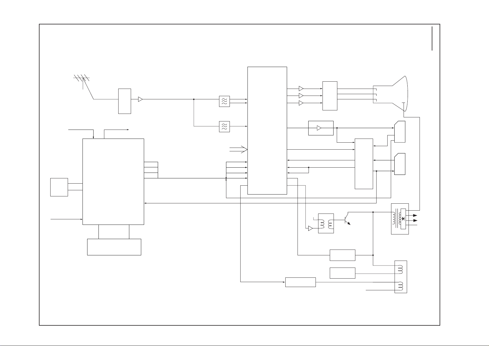
BLOCK DIAGRAM
This is a diagram for all models and therefore differs slightly from the actual block diagram.
Outline
IC803
MEMORY
PROTECT-IN
Aerial
PC-IN
SCL
SDA
Q701
Q711
Q721
Q242
Q243
Q244
VIDEO-OUT
R
G
B
R
G
B
CRT
A101
TUNER
Q141
X132
VIF
20
6
7
21
22
IC201
X131
SIF
POWER
26
25
I2C BUS
BLK
44
B
45
G
IC801
24
23
19
CPU
1 - 15
80 - 63
46
47
60
61
R
CVBS-IN
BLK
R
G
B
9
IF/VIDEO/
CHROMA/
34
35
15
16
17
18
26
DEF
54
3
43
39
40
41
32
C
Y
SYNC-IN
EW-OUT
H-OUT
Q431
Q121~Q133
T431
TV-IN
SIF-IN
C-OUT
Y-OUT
Refer also
to FIG.-2.
AV SELECTOR
NICAM DECODER
Q432
TV-OUT
AV1
13
8
15
18
SC-1
SC-2
AV2
MONTO
-OUT
T451
FBT
FOCUS
SCREEN
IC802
ROM
V-OUT IC501
6
PCC
CONTROL
CS
D.Y
H
CONTROL
3
V
Page 4
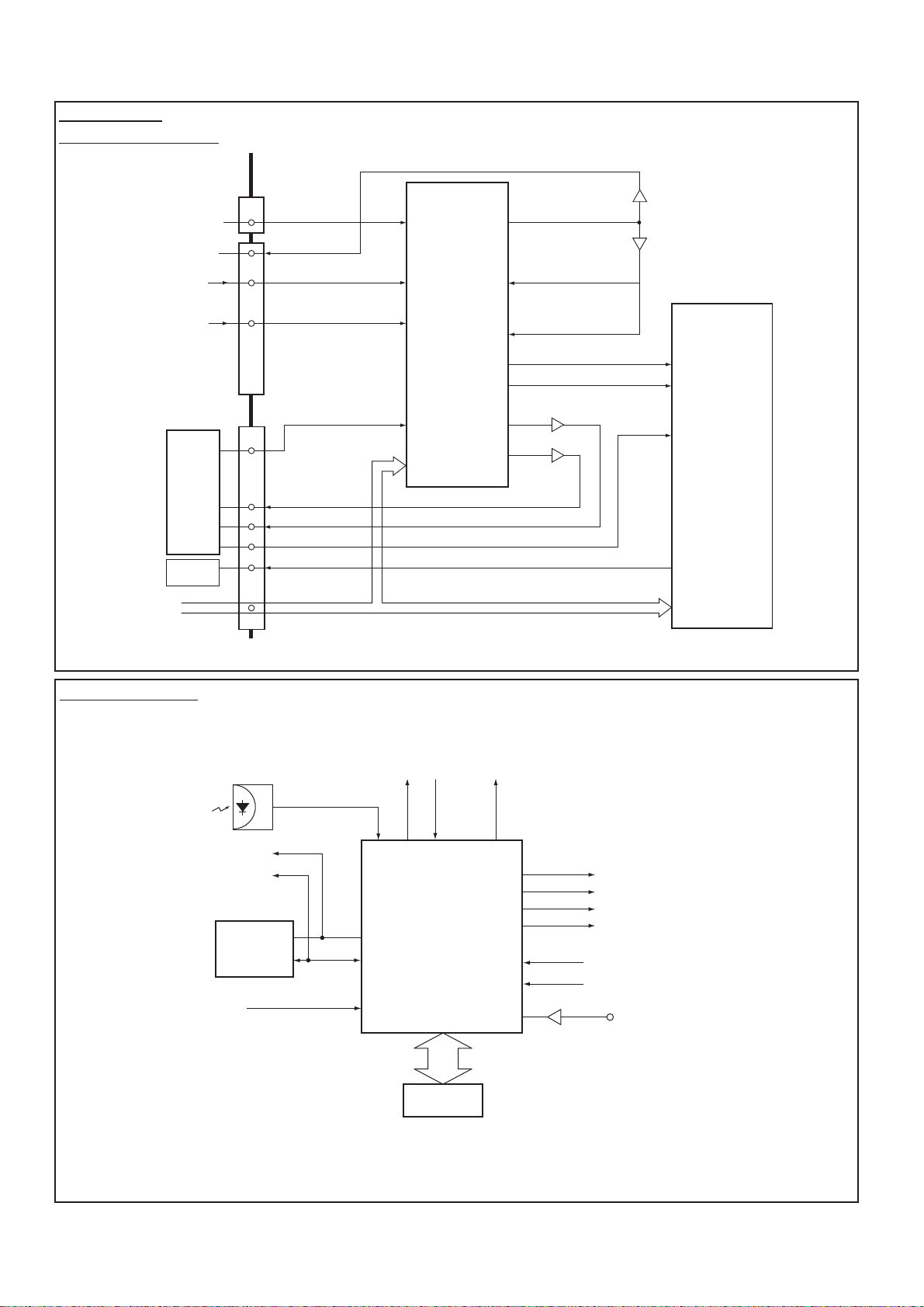
-4-
C2WYV
AV Selector
NICAM DECODER
System Control
Fig.-2
Fig.-3
FRONT-AV
SC-1
SC-2
IC201
IF/VIDEO/
CHROMA
IC001
AUDIO-OUT
I2C BUS
K12H
FRONT AV3
MONITOR-OUT
8
(VIDEO/AUDIO-L/R)
(VIDEO/Y/C/AUDIO-L/R)
K12J
(VIDEO)
13
15
C-OUT
18
Y-OUT
8
SIF-IN
5,6
AUDIO L/R-OUT
10,11
K12M
SC-1
SC-2
IC1201
AV-SELECTOR
<MM1313>
1(V)
2(L)
4(R)
13(V)
14(L)
16(R)
7(V)
8(L)
9(Y)
10(R)
11(C)
41(V)
19
20
SDA/SCL
(V)34
MONITOR-OUT
31
29
33
32
Y-OUT
37
C-OUT
38
Y-IN
C-IN
L-OUT
R-OUT
Q1204/1207
Q1205
Q1203
Q1202
AUDIO-OUT
IC3451
NICAM
37
&
36
STEREO
<TDA9875>
12
60
61
4
5
I2C BUS
CONTROL
IC803
MEMORY
RC-IN
SDA
POWER-FAIL
DETECT
SCL
POWER
25 31 28
24
23
43
1 - 7, 63 - 80
KEY-IN
IC801
CPU
IC802
ROM
Relay SW
39
44
45
46
BLK-OUT
B-OUT
G-OUT
R-OUT
36
37
60
61
SC1(AV1) 8-pin
SC2(AV2) 8-pin
Q806
CVBS
Page 5
-5-
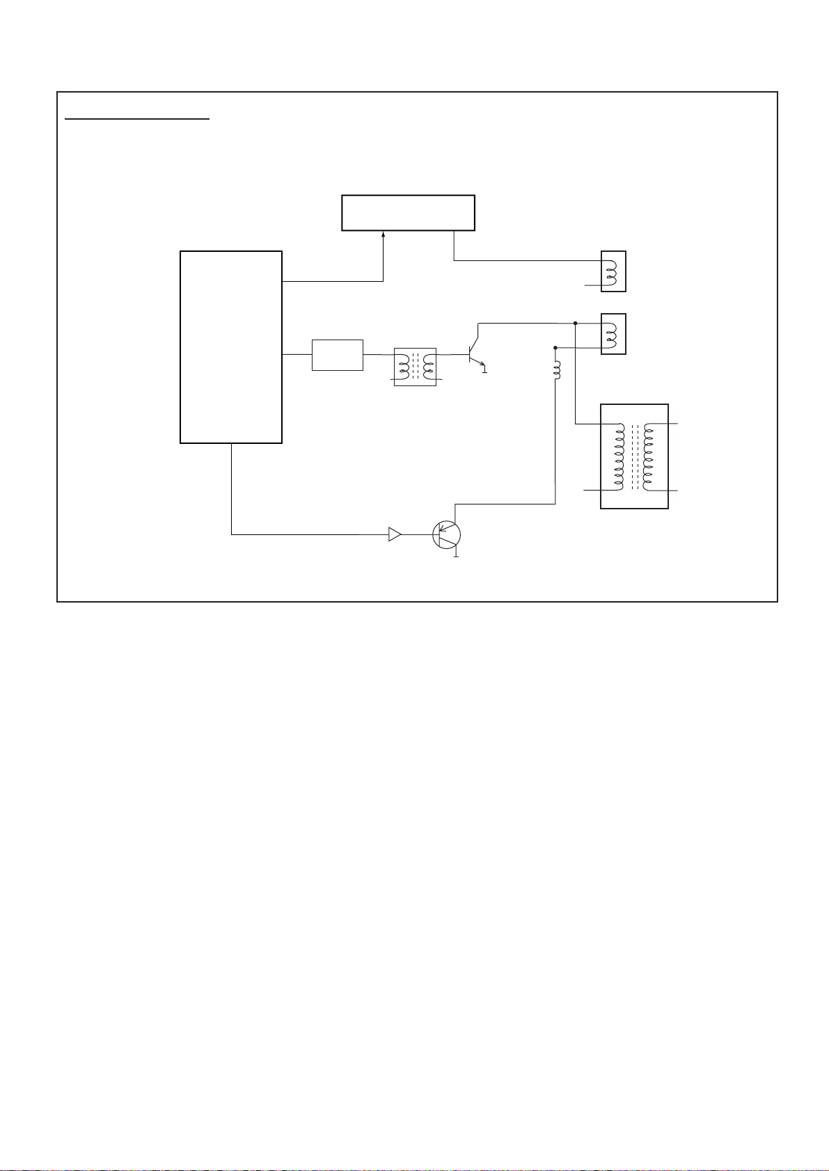
C2WYV
Deflection Control
IC501
V-Output<LA7833>
IC201
IF/VIDEO/
DEFLECTION
<TB1251>
41
EW-Out
63
Deflection
Yoke
26
32
V-Drive
Q431
H-Drive
Q431
H-Output
T431
Drive Trans
Vert.
Coil
Horiz.
Coil
T451
FlyBack Trans
L461/L462
Pcc Control
Q462
Q461
Page 6
-6-
C2WYV
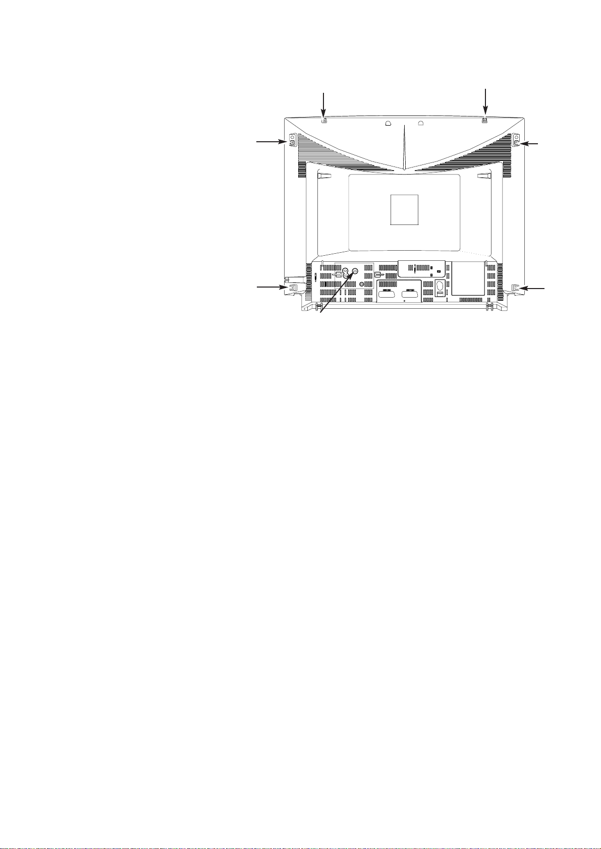
CABINET DISASSEMBLY
CABINET BACK DISASSEMBLY
1. Remove 7 screws(A).
2. Pull out the cabinet back.
(A)
(A)
(A)
(A)
(A)
(A)
(A)
Page 7
-7-
C2WYV
OPTION SETTING
[After replacing the Memory IC (IC803)]
The memory IC, IC803, stores the option data of TV set and service adjustments data for each circuit, therefore,
when the memory IC is replaced, it should be performed following setting and “SERVICE ADJUSTMENT” on next
page.
To enter to the Option Mode
+ Press and hold the F/OK button on the remote control and P▼ button on the front panel of the TV. The option
window will appear on the screen. Set the options as shown below.
To set the option mode
+ Highlight the desired option item by using the P▲ or P▼ button .
+ To switch the option mode, use the Volume - (LEFT) or Volume + (RIGHT) button.
+ The data which is set in the option mode is stored into the memory IC automatically.
Following table shows the available option items and default setting mode.
Exit from the Service Mode
+ Press the RECALL button.
Option Mode Mode Description & Note
ON-TIMER ON or OFF On-timer available, default “ON”
SORT MODE AUTO TUNE/SORT Tuning mode, default “AUTO TUNING”
or AUTO TUNING
or A TS EURO PLUS
PLUG & PLAY ON or OFF Plug & Play mode, default “ON”
WELCOME TEXT ON or OFF Display message when first set up, default “OFF”
CODE TEST OFF or ON For factory use, default “OFF”
WSS ON or OFF Wide Screen Signaling available, default “ON”
WIDE ON or OFF Wide mode, default “ON”
OPTION 4 or 7 LANGUAGE Language option , default “4 LANGUAGE”
312/313 Mode ON or OFF Teletext mode, default OFF
AV3 OPTION ON or OFF Front AV disable, default ON
3D SURROUND ON or OFF 3D Surround available, default ON
SIF OPTION BG, I, L/L’ or BG or BG/DK Television default system, Default “BG, I, L/L’”
OPTION SETTINGS FOR CE28DN7-C-00
OPTION
ON-TIMER ON
SORT MODE
PLUG & PLAY
WELCOME TEXT
CODE TEST
WSS
WIDE
OPTION
312/313 Mode
AV3 OPTION
3D SURROUND
SIF OPTION
AUTO VOLUME
ADJUST : EXIT : RECALL
AUTO TUNING
ON
ON
OFF
ON
OFF
4 LANGUAGE
ON
ON
ON
BG + DK
OFF
?
Page 8
-8-
C2WYV
SERVICE ADJUSTMENTS
[After replacing the Memory IC (IC803)]
The memory IC, IC803, stores the service adjustments data for each circuit, therefore, when the memory IC is
replaced, it should be programmed by using “OPTION SETTING” on previous page.
ADJUSTABLE SERVICE ADJUSTMENT
REGULAR
WIDE
To enter to the Service Mode
+ Press and hold the GREEN button on the remote control and then press the P▼ button inside of the door. The
adjustment window will appear on the screen.
IMPORTANT NOTICE
Do not attempt to adjust service adjustments not listed above otherwise it may cause loss of
performance and product safety.
Item No. OSD Description
1 P V-P Vertical Centre Adjustment
2 P H-P Horizontal Centre Adjustment
5 P V-S Vertical Size Adjustment
6 P H-S Horizontal Size Adjustment
7 P PCC Pcc Adjustment
8 P TRP Trapezoid Distortion Adjustment
10 P CNR Corner Adjustment
Item No. OSD Description
1 AGC AGC Adjustment
2 CUT Cut-Off Drive Adjustment
3 GRY G-Drive Adjustment
4 GRY B-Drive Adjustment
8 OSD OSD Positioning Adjustment
Note: Some items of the service adjustments for this chassis are controlled by the CPU, IC801, and the
adjustments are carried out by using the RC handset.
ADJUST
REGULAR
WIDE
OTHERS
TB1251
SELECT:
EXIT : RECALL
OK
Page 9

-9-
C2WYV
To select the mode and service item and change data value
+ Highlight the desired adjustment mode by using the P▲ or P▼ button and then press the F/OK button.
+ To select the adjustment item, use the P▲ or P▼ button.
+ To change the service data, use the Volume -(LEFT) or Volume + (RIGHT) button.
+ The data which is set in the service mode is stored into the memory IC automatically.
Exit from the Service Mode
+ Press the RECALL button or turn off the TV set by using the Mains switch.
INITIALISATION OF MEMORY IC
To initialise the memory IC (IC803), press and hold the NORMAL button on the remote control and then press
the P▲ button on the front panel of the TV set, and then turn the Mains switch Off and On. Now the initialisation is
completed.
When the memory IC is initialised, all of the service data (option data and service adjustment data) stored in the IC
are reset to the default value. It is necessary to readjust the service adjustments listed on pages 7 & 8.
REGULAR mode
WIDE mode
REGULAR
1, AGC 38
Adjustment No.
and Item name
Adjustment Data
Adjustment No.
and Item name
WIDE
1. P V-P 1F
Adjustment Data
Page 10
-10-
C2WYV
ADJUSTMENTS
IMPORTANT NOTICE
Do not attempt to adjust the following service adjustments except when adjustments are required in servicing
otherwise it may cause loss of performance and product safety.
1. Receive white raster pattern.
2. Set controls to normal.
3. Connect digital voltmetre to test point TP-B and GND.
4. Adjust voltage to 150 ±0.5V by using VR641.
1. Input and tune an RF signal which is UHF to the clearest station.
2. Connect digital voltmetre to test point TP-A and GND.
4. Enter to the service mode and select mode “REGU-
LAR”, and select item no.1 “REGULAR 1, AGC”.
5. Press the LEVEL+ or LEVEL - button to adjust volt-
age to be 3.2Vdc.
By using FOCUS VR, adjust focus control for well
defined scanning lines.
SCREEN ADJUSTMENT
1. Receive black & white pattern.
2. Enter to the service mode and select mode “REGU-
LAR”, and select item no. 2 “REGULAR 2, CUT”. The
horizontal line will appear on the screen.
3. Set the SCREEN VR for one colour to be just visible.
4. Using the numeric buttons shown set each colour to
minimum by decreasing to the point where any further
decrease resets the adjustment to maximum value.
BIAS ADJUSTMENT
5. By using the buttons 1, 2, 4, 5, 7, 8 on the remote
control, adjust the line to be white.
The key allocation is as follows;
Button No. Operation
1 Increase Red
2 Decrease Red
4 Increase Green
5 Decrease Green
7 Increase Blue
8 Decrease Blue
DRIVE ADJUSTMENT
6. Select item no.3 “REGULAR 3, GRY” (G-Drive) or 4
“REGULAR 4, GRY” (B-Drive) and adjust both initially
to 3F.
7. Change data value of each item by using
LEVEL + or
LEVEL - button to obtain the proper white balance.
PCC ADJUSTMENT
1. Receive cross hatch pattern and set screen mode to
“FULL”.
2. Enter to the service mode and select mode “WIDE”,
and select item no. 7 “WIDE 7.P PCC”.
3. Press the LEVEL+ or LEVEL - button to adjust the
vertical line to be straight.
TRAPEZOID ADJUSTMENT
1. Receive cross hatch pattern and set screen mode to
“FULL”.
2. Enter to the service mode and select mode “WIDE”,
and select item no. 8 “WIDE 8.P TRP”.
3. Press the LEVEL+ or LEVEL - button to correct the
trapezum distortion of the vertical line.
PCC ADJUSTMENT
GREY SCALE ADJUSTMENT
FOCUS ADJUSTMENT
AGC ADJUSTMENT
+ B VOLTAGE ADJUSTMENT
Page 11
-11-
C2WYV
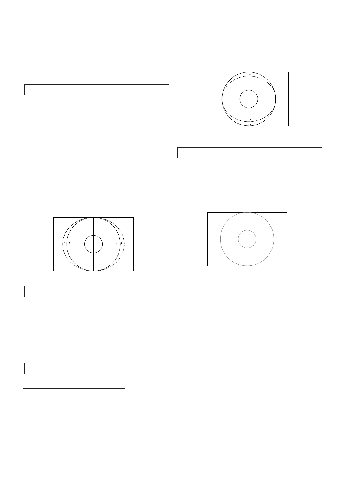
CORNER ADJUSTMENT
1. Receive cross hatch pattern and set screen mode to
“FULL”.
2. Enter to the service mode and select mode “WIDE”,
and select item no. 10 “WIDE 10.P CNR”.
3. Press the LEVEL+ or LEVEL - button to correct the
distortion of the vertical line around the corners.
HORIZONTAL CENTRING ADJUSTMENT
1. Receive circular pattern and set screen mode to
“FULL”.
2. Enter to the service mode and select mode “WIDE”,
and select item no. 2 “WIDE 2.P H-P”.
3. Press the LEVEL+ or LEVEL - button to adjust the
horizontal centre.
HORIZONTAL WIDTH ADJUSTMENT
1. Receive circular pattern and set screen mode to
“FULL”.
2. Enter to the service mode and select mode “WIDE”,
and select item 6 “WIDE 6.P H-W”.
3. Press the
LEVEL+ or LEVEL - button to adjust the
horizontal width.
1. Receive circular pattern and set screen mode to
“FULL”.
2. Set controls to normal.
3. Connect high-voltage meter to the anode of CRT and
GND.
4. Confirm that voltage is 26.0±1.0kV at 1.4mA for 28”
model.
VERTICAL CENTRING ADJUSTMENT
1. Receive circular pattern and set screen mode to
“FULL”.
2. Enter to the service mode and select mode “WIDE”,
and select item no. 1 “WIDE 1.P V-P”.
.3 Press the LEVEL+ or LEVEL - button to adjust the
vertical centre.
VERTICAL HEIGHT ADJUSTMENT
1. Receive circular pattern and set screen mode to
“FULL”.
2. Enter to the service mode and select mode “WIDE”,
and select item no. 5 “WIDE 5.P V-S.
3. Press the LEVEL+ or LEVEL - button to adjust the
vertical height.
1. Receive circular pattern and set screen mode to
“FULL”.
2. Enter to the service mode and select mode “REGULAR”, and select item no. 8 “REGULAR 8 OSD”. The
OSD test bar will appear on the top of screen.
3. Press the LEVEL+ or LEVEL - button to adjust prop-
er OSD positioning.
OSD POSITIONING ADJUSTMENT
VERTICAL ADJUSTMENT
HIGH-VOLTAGE CONFIRMATION
HORIZONTAL ADJUSTMENT
❚❚❚❚❚❚❚❚❚❚❚❚❚❚❚❚❚❚❚❚
Page 12

-12-
C2WYV
CPU PORT FUNCTIONS
Pin No. Function Name Function IN/OUT
1 MMU0 External memory 0 OUT
2 MMU3 External memory 3 OUT
3 ADDR10 Address bus 10 OUT
4 DSN Data Strobe
5 ADDR11 Address bus 11 OUT
6 ADDR9 Address bus 9 OUT
7 ADDR8 Address bus 8 OUT
8 RWN Read Write Strobe
9 GND
10 VDD Power Supply IN
11 OSC-IN Clock Input IN
12 OSC-OUT Clock Output OUT
13 ADDR13 Address bus 13 OUT
14 ADDR14 Address bus 14 OUT
15 MMU1 External memory 1 OUT
16 MMU2 External memory 2 OUT
17 MMU4 External memory 4 OUT
18 MMU5 External memory 5 OUT
19 P3.7/CSO Protect - Power failure detect input IN
20 P3.6/ASN Dolby CLK(L/L’) OUT
21 P3.5 Dolby SO(Super 3D) OUT
22 P3.4 PITTARI switch OUT
23 P5.1 IIC BUS SDA IN/OUT
24 P5.0 IIC BUS SCL OUT
25 P2.0 Remote Control Signal Input IN
26 P2.3 Power Relay & LED Drive On: L OUT
27 P2.4 SUB CPU SO OUT
28 P0.2 Key switch input IN
29 P0.1 SUB CPU CLK OUT
30 P0.0 SUB CPU SI IN
31 P4.7 THRESHOLD switch OUT
32 P4.6 JIMAKU(Caption) switch OUT
33 P4.5 On-Timer LED Drive ON: L OUT
34 VDD IN
35 GND
36 P2.1 AV1 Scart function input IN
37 P2.2 AV2 Scart function input IN
38 P2.5 RF AGC input IN
39 P4.4 H-Blank On/Off OUT
40 P4.3 AMP Mute Mute On: H OUT
41 P4.2 Dolby RQ OUT
42 P4.1 H-Blank Phase OUT
43 P4.0 50/60Hz output 50Hz: H OUT
44 FB BLK Output for OSD (Active H) OUT
45 B Blue Output for OSD (Active H) OUT
46 G Green Output for OSD (Active H) OUT
47 R Red Output for OSD (Active H) OUT
48 V-SYNC V-Sync Input (Active H) IN
49 H-SYNC H-Sync Input (Active H) IN
50 WSCR VPS/WSS Slicer Line PLL
Page 13

-13-
C2WYV
Pin No. Function Name Function IN/OUT
51 WSCF VPS/WSS Slicer Line PLL
52 VDD-A Analogue Power Supply IN
53 PXFM Pixel Frequency Multiplier
54 RESET Reset Input (Active L) IN
55 MCFM Pixel Frequency Multiplier
56 JTRSTO
57 TXCF
58 CVBS0
59 TEST0
60 CVBS1 Video signal Input IN
61 CVBS2 Video Signal Input IN
62 GND-A
63 DAT3 Data bus 3 IN
64 DAT4 Data bus 4 IN
65 DAT5 Data bus 5 IN
66 DAT6 Data bus 6 IN
67 DAT7 Data bus 7 IN
68 DAT2 Data bus 2 IN
69 DAT1 Data bus 1 IN
70 DAT0 Data bus 0 IN
71 ADDR0 Address bus 0 OUT
72 ADDR1 Address bus 1 OUT
73 ADDR2 Address bus 2 OUT
74 ADDR3 Address bus 3 OUT
75 ADDR4 Address bus 4 OUT
76 ADDR5 Address bus 5 OUT
77 ADDR6 Address bus 6 OUT
78 ADDR7 Address bus 7 OUT
79 ADDR12 Address bus 12 OUT
80 ADDR15 Address bus 15 OUT
Page 14

-14-
C2WYV
COMPONENT LOCATIONS
MAIN BOARD
KMA
IC801
UNDERSIDE OF BOARD
IC802
IC001
KMB
IC201
T131
KX
A101
TP-A
KM
KJ
K1001
T681
VR641
T611
Q613
IC501H2
IC501
IC501H3
K1002
Q432
TP-B
T451
Q461
Page 15

-15-
C2WYV
CRT BOARD
K7P
Q701
C735
K7D1
K7Q
Page 16

-16-
C2WYV
IC BLOCK DIAGRAMS
IC001 TDA7263M <Audio Output>
IC501 LA7833N <Vertical Output>
IN -L
IN +L
2
1
3
MUTE
CF COUPL
RF1 27K
-
L
+
SC
PROTECTION
10
OUT L
RF1
RF2
REFERENCES
SUPPLY
VOLTAGE
IN +R
IN -R
9
5
4
TURN-ON
AND-OFF
6
GND
VCC
6
+
R
-
RF1 27K
CF COUPL
Tj
TH
PROTECTION
TDA7263M
3
8
7
PUMP UP
OUT R
RF3
RF4
V-DRIVE PLS
INPUT
4
VERTICAL
DRIVE
15
GND
THERMAL
PROTECTION
VERTICAL
OUTPUT
2
V-OUTPUT
LA7833
Page 17

-17-
C2WYV
IC201 TB1251AN <IF/Video/Chroma/Def.>
H.AFC
FBP IN/SCP OUT
H Vcc(9V)
H OUT
Dig GND
SCL
SDA
BLACK Det
Dig.VDD
Sync in
Y IN
DC Restor
EW OUT
YC Vcc(5V)
+
ABCL IN
ref R
+
V OUT
V NFB
<V.SIZE>
<Sync det>
<Lock det.>
DEF Proc.
H,V synchronization
IF
I2C Bus
+
<AFC1 Gain>
<EHT.H>
<EHT.V>
EHT H/V
<H.SIZE>
EW PROC.
<EW PARA.>
<TRAPEZIUM>
V PROC.
<EW CONER>
<V.SHIFT>
<V.LINEAR.>
<V-S CORR.>
V RAMP
V BIAS
FILTER
BIAS
B OUT
G OUT
R OUT
+
>
γ
<
Y Proc.
Matrix / SW
Cutoff/Drive
<R.G.B.DRIVE>
<R.G.B.CUTTOFF>
YC GND
EXT.B IN
EXT.G IN
EXT.R IN
Y -D .L. <DL>
A.C. <P.SHARP>
Sub-Cont <S.CONT>
Uni-Color <CONT>
Bright <BRT>
WPS
Half T. <H.T>
<ABL START P>
Clamp
C-TRAP <c-trap>
Black Stretch <B.S.>
DC restore <DC rest>
+
Y-γ
<ABL GAIN>
Bright <RGB BRT>
RGB Interface
Uni-Color<RGB CONT>
Ys/Ym
C in
Cr in
Cb in
VSM OUT
AVSW
LOOP Filter
EHT in
DE-EMP.
TRAP
PIF tank
DC NF
PIF VCO
BIAS Filter
IF DET OUT
AFT OUT
Hcorr IN/SIF IN
RGB Vcc(9V)
+
CW OUT
4.43MHz X'tal
APC Filter
+
IF AGC
+
<Color>
<Unicolor>
Mode SW
Clamp
BBTINT
<TINT>
<F ID>
1 X'tal
1H delay line
<color system>
PAL/NTSC/SECAM
Chroma DEMOD .
+
<Killer Sence>
Chroma Baseband Proc.
SAW
RF AGC
L-SECAM
PIF Proc.
+
IF GND
1'st SIF IN
+
SAW
IF IN
AUDIO OUT
6.5MHz
Split SIF
Processor
Uni-SIF beet up
SIF OUT
Ripple F
56 505152535455 49 434445464748 42 363738394041 35 293031323334
FM DEMOD .
Gain Sw
L SECAM AM
<ATT>
AUDIO ATT
BIAS
IF Vcc(5V)
1 765432 8 14131211109 15 212019181716 22 282726252423
+
BPF
6.5MHz
Page 18

-18-
C2WYV
IC3451 TDA9875A <NICAM & Stereo Sound Decoder>
LOL
LOR
SCOL2
SCOR2
SCOL1
SCOR1
MOMOIN
EXTIL
EXTIR
SCIL2
SCIR2
SCIL1
SCIR1
PCLK
19
Vtune
NICAM
2
CAPR1
CAPL1
CAPL2
1
36
34
33
29
32
31
37
626352
514847
41
42
44
45
VDDA1
7
VSSA1
6
11
Vref1
Iref
8
CAPR2
PCAPR
54
PCAPL
55
CREST
CREST
Vref(n)
Vref(n)
Vref2
VSSG
VSSA2
VDDA2
59
56
403946
35
43
38
CREST
53
CREST
50
SIF1
SIF2
SCL
TIMING
DETECT DAC
TION
NICAM
DEMODULA-
TION
FM(AM)
DEMODULA-
TION
IDENTIFICA-
5
SDA
NICAM
DEMATRIXCLOCK
181721
XTALI
XRALO
DECODER
SYSCLK
SWITCH
ANALOG
SCROSSBAR
LEVEL
ADJUST
LEVEL
ADJUST
PEAK
DETECTION
27
2625242223
SDI1
SDI2
ADC(2)
AUDIO
I2C BUS
INTERFACE
SDO1
SDO2
SCK
SELECT
DIGITAL
1564144916
WS
VDDD1
VDDD2
DAC(2)
DIGITAL
SUPPLY
VSSD1
VSSD2
CREST
DAC
SUPPLY
AUDIO PROCESSING
SUPPLU DAC
DAC(2)
DAC(2)
TEST
30
28
TEST1
TEST2
SUPPLY
REFERENCE
OPERATIONAL
TDA9875
AMPLIFIERS
57
58
60
61
AUXOR
AUXOL
MOR
MOL
(SIF)
SUPPLY
SOUND IF
12
9
20
P1
AGC, ADC
INPUT SWITCH
I2C BUS
INTERFACE
3
4
13
P2
ADDR2
ADDR1
10
Page 19

-19-
C2WYV
C2WYV
PIN DESCRIPTION OF SEMICONDUCTORS
● Diode
● Transistor/FET
● IC
FET
● Diode
K
A
● Transistor/FET
K
A
K
AA
KK
A
K
K
K: Cathode
A: Anode
A
A
C
B
C
E
● IC
1
E
3
2
Index
C1
3
E
C2
Vdd
2
1
C1
B1 B2
E
B2
GND
C2
C
C
E
B
C
E
B
B
2
3
1
E
C1
CBE
C2
B2
E
3
2
C
B
B1
1
C
BE
B1
RESET
Index
1
2
N
1
2
N
C2
E2 C1
B1
B2
B1
B2
(IN)
E1
1
(GND)
2
4
5
6
Index
E1
C1
C2
E2
3
(OUT)
C: Collector
B: Base
E: Emitter
G
3
2
1
Index
D: Drain
G: Gate
S: Source
S
G
D
S
D
3
21
5
4
Index
N
1
Index
Index
Index
N
1
N
1
N
1
Index
N
1
N
1
Index
Page 20
-20-
C2WYV
PARTS DESCRIPTION AND READING IN SCHEMATIC DIAGRAM
1. The parts specification of resistors, capacitors and
coils are expressed in designated code. Please
check the parts description by the following code
table.
2. Some of transistors and diodes are indicated in
mark for the substitution of parts name. Please
check the parts name by the following code table.
3. Voltages and waveforms were taken with a video
colour bar signal(1Vp-p at 75 ohms terminated) and
controls to normal.
4. Voltages were taken with a high-impedance digital
voltmetre.
Example 2000 K K 1000 BG
Characteristic
Example 160 E M 10
Capacitance value
Tolerance
Type
Rated voltage
Excepting electric capacitors, all
capacitance values of less than 1
are expressed in µF and more
than 1 are in pF.
Example L2 C1 4R7 K N
Tolerance
Inductance value
Manufacture code
Unique code
Mark Material
E Electrolytic
P Electrolytic (non-Polarised)
C Ceramic (temperature compensation)
K Ceramic
F Polyester
N Polypropylene
M Metalised polypropylene
H Metalised polypromylar
B Ceramic (semiconductor)
G Metalised polyester
Y Composite film
S Styrol
T Tantalum oxide solid electrolytic
U Organic semiconductive electrolyte
D Electric double layer electrolytic
Mark Tolerance
A not specified
B ±0.1
C ±0.25
D ±0.5
F±1
G±2
E ±2.5
H±3
J±5
K±0
M±20
N±30
P +100 -0
Q +30 -10
T +50 -10
U +75 -10
V +20 -10
W +100 -10
X +40 -20
Y +150 -10
Z +80 -20
Mark Tolerance (nH) Mark Tolerance (%)
C ±0.25 G ±2
D ±0.5 J ±5
S ±0.3 K ±10
A ±0.2 L ±15
M±20
Coil Reading
Capacitor Reading
Example 1/2 D J 10K B
Example 6 W K 8.2
Example 1/2 C K 1M
Resistor Reading
Characteristic
Z (Carbon fuse)
B (Non-burnable)
Resistance value
Tolerance (see below table)
Material (see below table)
Rated wattage (W)
K indicates in KΩ
M indicate in MΩ
Note: Resistor which is indicated with resistance value only are
1/6W carbon resistor. Resistor which is indicated with material, tolerance and value are 1/4W rated wattage.
Mark Material
D Carbon
N Metal film
S Oxide metal film
C Solid
G Metal glaze
W Wire wounding or cement
H Ceramic
F Fusible
Mark Tolerance
A ±0.05
B ±0.1
C ±0.25
D ±0.5
F±1
G±2
J±5
K±10
M±20
P +5 -15
Z used in 0 ohm
● Material table
● Tolerance table
● Material table
● Tolerance table
Mark Type number
-- 1S1555,1S2473,1S2076,1SS133,DS442,1SS176
K 1S1555,1S2473,1S2076,DS442
L 1S1555,1S2076A,1S2471
M 1SS133,1SS176,GMA01
N 1S1555,1S2473,1S2076,1SS133,DS442,1SS176,1N4148
P 1S1555,1S2076A,1S2471,1N4148
R 1S1555,1S2076,1S2473,DS442,1N4148
AA 1S1555,1S2076,1S2473,1SS133,DS442,1SS176,1N4148,GMA01
● Diode
Mark Type number
-- 2SC536 2SC945A 2SC1815 2SC1740 2SC1740S KSC945C
A E, F, G P, Q, R O, Y, G Q, R, S Q, R, S
B E, F, G P, Q, R O, Y, G Q, R, S
D F, G P, Q Y, G Q, R, S
F F, G P G R, S
H F, G P, Q Y, G Q, R, S Y, G
I E, F, G P, Q, R O, Y, G Q, R, S Y, G
G F, G P G R, S G
AD F, G Q, R Y, GR Q, R, S
AE E, F, G Q, R O, Y, GR Q, R, S
● Transistor (NPN type)
Mark Type number
-- 2SA608 2SA564A 2SA1015 2SA933 2SA933S KSA733C
Y E, F Q, R O, Y, G Q, R
WF R Y, GR
V E, F Q, R O, Y, G Q, R Y, G
U F R Y, G R G
Z E, F Q, R O, Y, G Q, R Q, R
AB F R Y Q, R
AE E, F Q, R O, Y R
● Transistor (PNP type)
Diode/Transistor Type Reading
Page 21

-21-
C2WYV
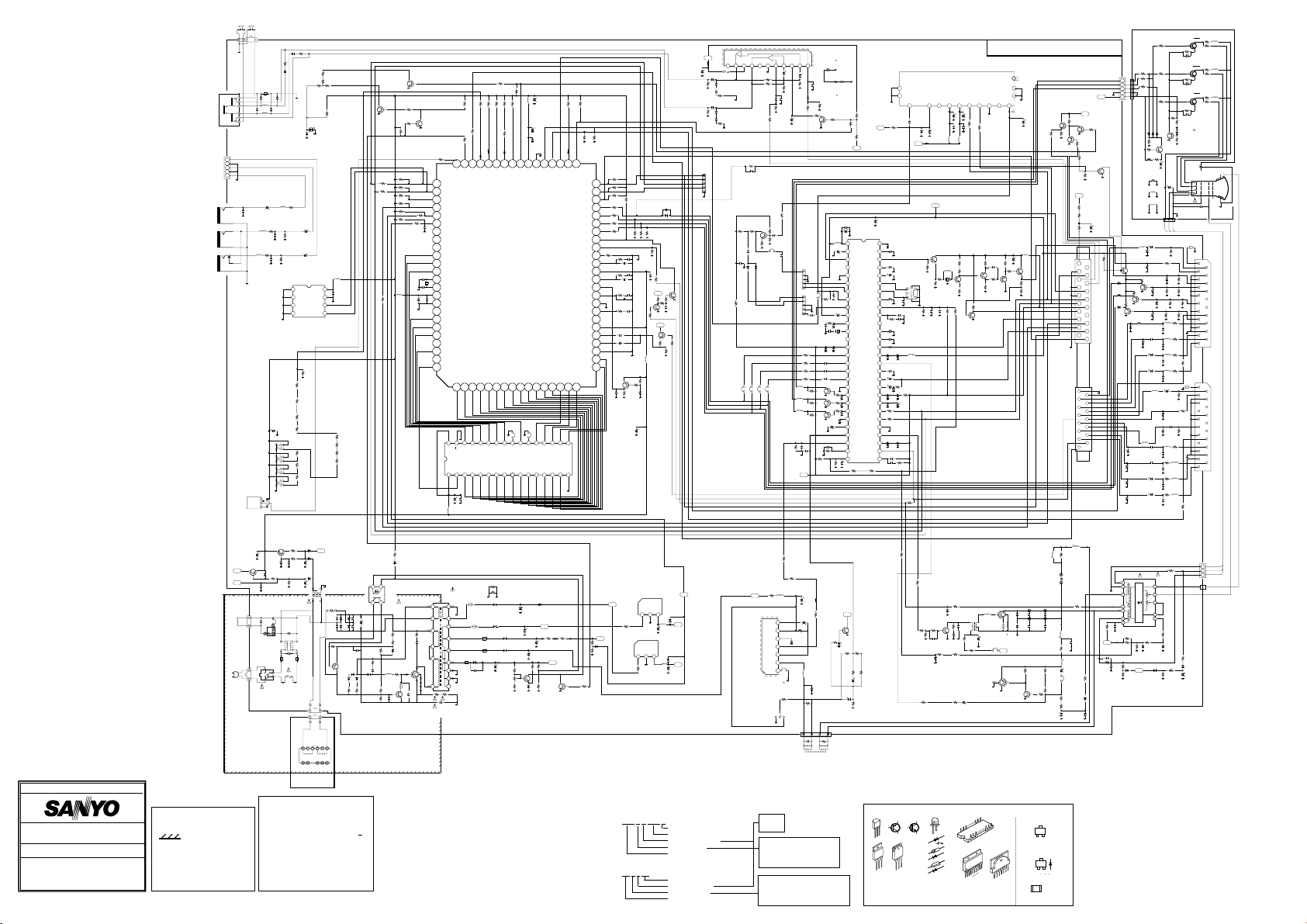
CABINET PARTS LIST FOR MODEL CE28DN7-C-00
Note: Parts order must contain Service Ref. No., Part No., and descriptions.
1
2
6
4
7
8
9
3
5
Ref. No. Part No. Description Ref. No. Part No. Description
CABINET PARTS
1 1AA0CAM0258-F ASSY,CABINET FR-C2WR
2 610 276 5618 BUTTON POWER-F7WC
3 610 286 7725 CABINET BACK G-F7WA
4 1AA2DDM00921A DOOR-C2WY
5 610 276 5656 DEC IND-F7WC
6 610 261 3032 SPRING-E7GC
7 645 043 5058 BADGE,SANYO*53.5X12L53.3
8 645 019 2449 PUSH LATCH 7.9X6.9BK
ACCESSORIES
9 JXMTA RC TRANSMITTER
SKP10326 INST MANUAL-C2WYV (1)
SKP10327 INST MANUAL-C2WYV (2)
SKP10328 INST MANUAL-C2WYV (3)
SKP20350 SHEM DIAG -C2WYV-00
645 027 6927 BATTERY
Page 22
-
C2WYV
-22-
CHASSIS ELECTRICAL PARTS LIST
Product safety should be considered when a component replacement is made in any area of a receiver.
Components indicated by a mark in this parts list and the circuit diagram show components whose value have
special significance to product safety. It is particularly recommended that only parts specified on the following
parts list be used for components replacement pointed out by the mark .
1AA0B10H050U0 ASSY,PWB,MAIN C2WYV
CAPACITOR
C001 403 314 5915 SMD CAP GRM40X7R474K16
C002 403 215 2310 CERAMIC 0.012U K 50V
C003 403 314 5915 SMD CAP GRM40X7R474K16
C004 403 215 2310 CERAMIC 0.012U K 50V
C005 403 258 3619 25 YK 33 M TA 0511
C006 403 258 3619 25 YK 33 M TA 0511
C007 403 164 0214 CERAMIC 0.1U Z 25V
C008 403 164 0214 CERAMIC 0.1U Z 25V
C009 403 164 0214 CERAMIC 0.1U Z 25V
C010 403 164 0214 CERAMIC 0.1U Z 25V
C011 403 190 4702 ELECT 1000U M 50V
C012 403 190 4702 ELECT 1000U M 50V
C015 403 047 5065 ELECT 470U M 25V
C021 403 154 1917 35 YK 1000 M TA K1220
C052 403 113 3815 CERAMIC 1000P K 50V
C053 403 149 9218 CERAMIC 0.01U Z 50V
C054 403 068 9016 CERAMIC 100P K 50V
C1001 401 105 7919 MT-GLAZE 0.000 ZA 1/16W
C101 403 233 1517 50 YK 4R7 M TA 0511
C1010 403 157 3611 CERAMIC 100P J 50V
C1011 403 279 4312 CERAMIC 0.33U K 16V
C1012 403 157 3611 CERAMIC 100P J 50V
C1013 403 279 4312 CERAMIC 0.33U K 16V
C1014 403 113 3815 CERAMIC 1000P K 50V
C1015 403 233 0817 ELECT 10U M 50V
C1016 403 113 3815 CERAMI 1000P K 50V
C1017 403 189 2425 ELECT 16MS7 10M TZ 0407
C1018 401 105 7919 MT-GLAZE 0.000 ZA 1/16W
C102 403 039 3527 ELECT 470U M 6.3V
C1020 403 149 9218 CERAMIC 0.01U Z 50V
C1021 403 157 3611 CERAMIC 100P J 50V
C1022 403 279 4312 CERAMIC 0.33U K 16V
C1024 403 157 3611 CERAMIC 100P J 50V
C1025 403 279 4312 CERAMIC 0.33U K 16V
C1026 403 113 3815 CERAMIC 1000P K 50V
C1027 403 233 0817 ELECT 10U M 50V
C1028 403 113 3815 CERAMIC 1000P K 50V
C1029 403 233 0817 ELECT 10U M 50V
C103 403 039 3527 ELECT 470U M 6.3V
C104 403 233 0817 ELECT 10U M 50V
C1042 401 105 7919 MT-GLAZE 0.000 ZA 1/16W
C1043 401 105 7919 MT-GLAZE 0.000 ZA 1/16W
C1044 401 105 7919 MT-GLAZE 0.000 ZA 1/16W
Ref. No.
Part No.
Description
Chassis construction
CE28DN7-C-00
1AA0B10H050U0 ASSY,PWB,MAIN C2WYV (Page 24~29)
1AA0B10H043L0 NO 3D. NIC.SW.C2KRV (Page 29~30)
1AA0B10E59500 ASSY,PWB,CRT C2WC (Page 30~31)
1AA0B10H047B0 ASSY,PWB,HARMONICS EB6 AC (Page 31)
OUT OF CIRCUIT-013C2WVV (Page 31)
Read description in the Capacitor and Resistor as follows:
CAPACITOR
CERAMIC 100P K 50V
Tolerance Symbols:
Less than 10PF
A: Not specified B: ±0.1PF C: ±0.25PF
D: ±0.5PF F: ±1PF G: ±2PF
R: ±0.25-0PF S: ±0-0.25PF E: +0-1PF
More than 10PF
A: Not specified B: ±0.1% C: ±0.25%
D: ±0.5% F: ±1% G:±2%
H: ±3% J: ±5% K: ±10%
L: ±15% M: ±20% N: ±30%
P: +100-0% Q: +30-10% T: +50-10%
U: +75-10% V: +20-10% W:+100-10%
X: +40-20% Y: +150-10% Z: +80-20%
Material:
CERAMIC............Ceramic
MT-PAPER ..........Metallized Paper
POLYESTER ......Polyester
MT-POLYEST ......Metallized Polyester
POLYPRO............Polypropylene
MT-POLYPRO ....Metallized Polypropylene
COMPO FILM......Composite film
MT-COMPO ........Metallized Composite
STYRENE............Styrene
TA-SOLID............Tantalum Solid
AL-SOLID............Aluminium Solid
ELECT ................Electrolytic
NP-ELECT ..........Non-polarised Electrolytic
OS-SOLID ..........Aluminium Solid with Organic Semiconductive Electrolytic
DL-ELECT ..........Double Layered Electrolytic
RESISTOR
CARBON 4.7K J A 1/4W
Rated Wattage
Performance Symbols:
A: General B: Non flammable Z: Low noise
Other: Temperature coefficient
Material:
CARBON Carbon
MT-FILM Metal Film
OXIDE-MT Oxide Metal Film
SOLID Composition
MT-GLAZE Metal Glaze
WIRE WOUND Wire Wound
CERAMIC RES Ceramic
FUSIBLE RES Fusible
Rated Voltage
Rated value: P=pico farad, U=Micro farad
Note: Parts order must contain Service Ref. No., Part No., and descriptions.
Tolerance Symbols:
A: ±0.05% B: ±0.1%
C: ±0.25% D: ±0.5%
F: ±1% G: ±2%
J: ±5% K: ±10%
M: ±20% P: +5-15%
Rated value, ohms:
K: 1,000, M: 1,000,000
!
!
Page 23

-23-
C2WYV
Ref. No. Part No.
Part No.
Description
Ref. No.
Description
C1050 403 157 3611 GRM1885C1H101JZ01D PT115
C106 403 149 9218 CERAMIC 0.01U Z 50V
C109 403 149 9218 CERAMIC 0.01U Z 50V
C110 403 149 9218 CERAMIC 0.01U Z 50V
C1102 403 113 3815 CERAMIC 1000P K 50V
C1107 403 113 3815 CERAMIC 1000P K 50V
C1108 403 233 0817 ELECT 10U M 50V
C1109 403 233 0817 ELECT 10U M 50V
C1110 403 166 9215 CERAMIC 10P J 50V
C121 403 149 9218 CERAMIC 0.01U Z 50V
C122 403 164 0214 CERAMIC 0.1U Z 25V
C124 403 157 1518 CER.GRM39COG3R0C50PT
C125 403 069 8315 CERAMIC 0.01U Z 50V
C128 403 241 3817 10 YK 220 M TA 0511
C130 403 157 2515 CERAMIC 27P J 50V
C131 403 149 9218 CERAMIC 0.01U Z 50V
C135 403 149 9218 CERAMIC 0.01U Z 50V
C136 403 149 9218 CERAMIC 0.01U Z 50V
C138 403 149 9218 CERAMIC 0.01U Z 50V
C139 403 237 7941 MT-COMPO 0.22U J 50V
C140 403 233 0817 ELECT 10U M 50V
C141 403 207 0317 SMD 1MF GRM40Y5V105Z16PT
C143 401 105 7919 MT-GLAZE 0.000 ZA 1/16W
C144 403 248 2813 50 YK 2R2 M TA 0511
C145 403 149 9218 CERAMIC 0.01U Z 50V
C146 403 248 1618 16 YK 47 M TA 0511
C1900 403 038 1633 ELECT 100U M 6.3V
C1921 403 149 9218 CERAMIC 0.01U Z 50V
C1922 403 149 9218 CERAMIC 0.01U Z 50V
C1923 403 149 9218 CERAMIC 0.01U Z 50V
C1924 403 149 9218 CERAMIC 0.01U Z 50V
C1925 403 085 7405 NP-ELECT 10U M 16V
C1926 403 085 7405 NP-ELECT 10U M 16V
C201 403 149 9218 CERAMIC 0.01U Z 50V
C203 403 269 5916 CERAMIC 0.22U K 16V
C204 403 149 9218 CERAMIC 0.01U Z 50V
C205 403 149 9218 CERAMIC 0.01U Z 50V
C206 403 149 9218 CERAMIC 0.01U Z 50V
C207 403 149 9218 CERAMIC 0.01U Z 50V
C208 403 248 1618 16 YK 47 M TA 0511
C209 403 164 0214 CERAMIC 0.1U Z 25V
C210 403 086 2300 NP-ELECT 1U M 50V
C211 403 113 3815 CERAMIC 1000P K 50V
C212 403 086 2300 NP-ELECT 1U M 50V
C213 403 233 0817 ELECT 10U M 50V
C214 403 149 9218 CERAMIC 0.01U Z 50V
C216 403 233 0817 ELECT 10U M 50V
C217 403 160 0020 ELECT 470U M 10V
C218 403 149 9218 CERAMIC 0.01U Z 50V
C219 403 155 2418 CERAMIC 5600P K 50V
C220 403 207 0317 SMD 1MF GRM40Y5V105Z16PT
C230 403 269 5916 CERAMIC 0.22U K 16V
C231 403 113 4119 CERAMIC 2200P K 50V
C232 403 233 3818 CERAMIC 10P C 50V
C233 403 248 1618 16 YK 47 M TA 0511
C234 403 164 0214 CERAMIC 0.1U Z 25V
C235 403 164 0214 CERAMIC 0.1U Z 25V
C236 403 164 0214 CERAMIC 0.1U Z 25V
C237 403 164 0214 CERAMIC 0.1U Z 25V
C240 403 113 4119 CERAMIC 2200P K 50V
C241 403 067 7895 MT-COMPO 0.47 J 50V
C242 403 257 0817 50 YK 0R47 M TA 0511
C243 403 071 2912 CERAMIC 1800P K 50V
C244 403 215 2211 CERAMIC 0.01U K 50V
C247 403 233 0817 ELECT 10U M 50V
C251 403 314 5915 SMD CAP GRM40X7R474K16
C252 403 314 5915 SMD CAP GRM40X7R474K16
C421 404 074 7802 MT-POLYPRO 4000P H 1.5K
C422 403 299 3210 POLYPRO 0.027U J 400V
C423 404 074 3903 MT-POLYPRO 8000P J 1.5K
C424 403 083 3201 POLYPRO 0.012U J 400V
C431 403 068 5612 CERAMIC 0.056U Z 25V
C432 403 075 7111 CERAMIC 1000P K 500V
C433 403 076 3112 CERAMIC 3900P K 500V
C434 403 054 0703 ELECT 47U M 35V
C437 403 066 6106 MT-POLYEST 0.47U J 250V
C441 403 309 2100 POLYPRO 0.3U J 400V
C445 403 233 0817 ELECT 10U M 50V
C450 404 056 5208 NP-ELECT 100NW2R2MTA-6311
C451 404 063 5703 NP-ELECT 100NW1R0MTA-6311
C463 403 307 6506 POLYESTER 6800P K 100V
C466 403 188 0808 MT-POLYEST 2.2U J 100V
C468 403 233 1111 ELECT 22U M 50V
C481 403 076 1415 CERAMIC 2700P K 500V
C482 403 159 7409 MT-POLYEST 0.1U K 250V
C501 403 194 3800 ELECT 2200U M 25V
C502 403 217 1103 ELECT 220U M 35V
C503 403 139 7514 CERAMIC 39P J 50V
C512 403 218 8200 ELECT 2200U M 25V
C513 403 233 0817 ELECT 10U M 50V
C514 403 233 0817 ELECT 10U M 50V
C600 403 076 4010 CERAMIC 4700P K 500V
C601 404 060 7205 MT-POLYEST 0.1U M 250V
C602 404 060 7205 MT-POLYEST 0.1U M 250V
C603 403 076 7130 CERAMIC 1000P M 1K
C604 403 076 7130 CERAMIC 1000P M 1K
C605 403 076 7130 CERAMIC 1000P M 1K
C606 403 076 7130 CERAMIC 1000P M 1K
C607 404 079 8002 ELECT LP5-400V151MS24Z1
C613 403 179 1213 POLYESTER 4700P J 50V
C614 403 237 8057 MT-COMPO 0.1U J 50V
C615 403 179 3217 POLYESTER 0.015U J 50V
C616 403 165 6215 CERAMIC 1000P K 2K
C617 403 179 2418 POLYESTER 0.022U K 50V
C631 404 073 4505 CERAMIC DE1210-1 E 222M
C633 403 054 1502 ELECT 470U M 35V
C636 403 190 3705 ELECT 1000U M 16V
C637 403 053 3606 ELECT 2200U M 35V
C640 403 218 8200 ELECT 2200U M 25V
C641 403 076 6727 CERAMIC DE0607-486B102K1K
C642 404 055 9801 ELECT 220U M 200V
C643 403 190 4702 ELECT 1000U M 50V
C647 403 157 6810 CERAMIC 680P K 50V
C648 403 039 3507 ELECT 470U M 6.3V
C649 403 194 4609 ELECT 470U M 16V
C681 403 148 0424 ELECT 1000U M 25V
C682 403 069 9510 CERAMIC CHIP 0.01Z 50V
C683 403 039 9004 ELECT 1000U M 10V
C684 403 135 7815 50 YK 3R3 M TA 0511
C800 403 248 1618 16 YK 47 M TA 0511
C801 403 149 9218 CERAMIC 0.01U Z 50V
C806 403 248 1618 16 YK 47 M TA 0511
C807 403 164 0214 CERAMIC 0.1U Z 25V
C810 403 269 5916 CERAMIC 0.22U K 16V
C811 403 269 5916 CERAMIC 0.22U K 16V
C812 403 157 4212 CERAMIC 220P J 50V
C814 403 155 2210 CERAMIC 3300P K 50V
C816 403 155 2319 CERAMIC 4700P K 50V
C817 403 145 9915 CERAMIC 22P J 50V
C818 403 155 2319 CERAMIC 4700P K 50V
C819 403 145 9915 CERAMIC 22P J 50V
C822 403 113 4119 CERAMIC 2200P K 50V
C824 403 153 9310 CERAMIC 82P J 50V
C826 403 086 1808 NP-ELECT 0.47U M 50V
C827 403 314 5915 SMD CAP GRM40X7R474K16
C828 403 149 9218 CERAMIC 0.01U Z 50V
C829 403 248 1618 16 YK 47 M TA 0511
C830 403 157 6711 CERAMIC 560P K 50V
C831 403 164 0214 CERAMIC 0.1U Z 25V
C832 403 248 1618 16 YK 47 M TA 0511
!
Page 24

-24-
C2WYV
Ref. No.
Part No.
Description
Ref. No.
Part No.
Description
C833 403 157 2515 CERAMIC 27P J 50V
C834 403 157 2515 CERAMIC 27P J 50V
C835 403 155 2319 CERAMIC 4700P K 50V
DIODE
D1001 407 221 7116 ZENER D. UDZS-TE-1712B
D1002 407 221 7116 ZENER D. UDZS-TE-1712B
D1003 407 221 7116 ZENER D. UDZS-TE-1712B
D1004 407 063 8319 ZENER DIODE MTZJ11C
D1007 407 221 7116 ZENER D. UDZS-TE-1712B
D1008 407 221 7116 ZENER D. UDZS-TE-1712B
D1009 407 063 8319 ZENER DIODE MTZJ11C
D101 407 100 0214 ZENER DIODE MTZJ36A
D1010 407 221 7116 ZENER D. UDZS-TE-1712B
D1011 407 149 0817 DIODE 1SS355-TE-17
D1012 407 149 0817 DIODE 1SS355-TE-17
D1013 407 149 0817 DIODE 1SS355-TE-17
D1021 407 063 8319 ZENER DIODE MTZJ11C
D1022 407 063 8319 ZENER DIODE MTZJ11C
D1023 407 063 8319 ZENER DIODE MTZJ11C
D1024 407 063 8319 ZENER DIODE MTZJ11C
D1025 407 063 8319 ZENER DIODE MTZJ11C
D1026 407 063 8319 ZENER DIODE MTZJ11C
D1901 407 120 9706 LED LN28RPL
D1901A 610 222 0322 LED HOLDER-G2CA-A
D1906 407 063 9514 ZEN DIODE
D431 407 063 9613 ZENER DIODE MTZJ9.1A
D438 407 095 8001 DIODE ERD07-15L
D439 407 006 4128 DIODE ERB44-04V1
D442 408 007 8607 DIODE 1N4148
D445 407 012 4416 DIODE 1SS133-T-77
D446 407 063 9415 ZENER DIODE MTZJ8.2A
D463 407 012 4416 DIODE 1SS133-T-77
D466 407 099 7812 ZENER DIODE MTZJT-77-20A
D469 407 007 7415 DIODE EU1
D481 407 007 7415 DIODE EU1
D482 407 012 4416 DIODE 1SS133-T-77
D501 407 005 7328 DIODE EM01Z
D502 407 118 2217 ZENER DIODE 1Z75
D603 407 009 6921 DIODE RM11C
D604 407 009 6921 DIODE RM11C
D605 407 009 6921 DIODE RM11C
D606 407 009 6921 DIODE RM11C
D613 407 012 4416 DIODE 1SS133-T-77
D614 408 007 8607 DIODE 1N4148
D615 407 173 2907 PHOTO COUPLE PC123F2
D616 408 007 8607 DIODE 1N4148
D617 407 007 6616 DIODE ES1
D618 408 007 8607 DIODE 1N4148
D619 407 063 8319 ZENER DIODE MTZJ11C
D630 407 007 7613 DIODE EU2
D633 407 166 2303 DIODE ERC-91-02L
D634 407 007 7613 DIODE EU2
D635 407 129 6706 DIODE RU4YX LF-L1
D637 407 012 4416 DIODE 1SS133-T-77
D641 407 012 4416 DIODE 1SS133-T-77
D642A 407 009 8816 DIODE RU3AM
D643 407 012 4416 DIODE 1SS133-T-77
D645 407 099 5511 ZENER DIODE MTZJ6.2C
D681 407 005 7328 DIODE EM01Z
D682 407 063 8913 ZENER DIODE MTZJ5.6C
D683 407 005 7328 DIODE EM01Z
D684 408 007 8607 DIODE 1N4148
D685 407 012 4416 DIODE 1SS133-T-77
D826 407 099 4811 ZENER DIODE MTZJ4.3B
D831 407 149 0817 DIODE 1SS355-TE-17
INTERGRATED CIRCUITS
IC001 409 301 4906 IC TDA7263M
IC001-1 610 251 4186 AUDIO HEATSINK ASSY E7PC
IC201 409 504 3300 IC TB1251CN VER 6.3
IC501 409 192 5709 IC LA7833
IC641 409 241 5407 IC BA178M05T
IC642 409 377 5401 IC L78M09CV ST
IC801 410 329 1600 IC ST92R195
IC802 QXXAAJQ0279B- C2KZV VP/P DD54
IC803 409 343 6302 IC 24LC04B/P
TRANSFORMER
T431 610 000 1077 DRIVE TRANS
T451 645 038 7616 TRANS,FLYBACK
T611 645 041 2240 TRANS,POWER,PULSE
T681 610 033 3758 POWER TRANS
COIL
L1003 610 078 5946 PIPE CORE
L1010 645 001 4550 PEAKING COIL 10UHK
L1011 645 001 4550 PEAKING COIL 10UHK
L1012 645 001 4550 PEAKING COIL 10UHK
L1013 645 001 4550 PEAKING COIL 10UHK
L1017 610 078 5946 PIPE CORE
L1020 645 001 4550 PEAKING COIL 10UHK
L1021 645 001 4550 PEAKING COIL 10UHK
L1022 645 001 4550 PEAKING COIL 10UHK
L1023 645 001 4550 PEAKING COIL 10UHK
L1101 645 001 4550 PEAKING COIL 10UHK
L1106 645 001 4550 PEAKING COIL 10UHK
L121 645 001 5526 COIL 6.8UK LAPO2TA6R8K
L123 401 016 9821 CARBON 27JA 1/4W FLAM-RET
L171 645 040 2715 TRANS,OSC 38.9MHZ
L1921 645 008 5635 INDUCTOR,12U K
L1922 645 008 5635 INDUCTOR,12U K
L1923 645 002 4511 CORE,PIPE
L240 645 001 4550 PEAKING COIL 10UHK
L241 645 001 4550 PEAKING COIL 10UHK
L242 645 001 4550 PEAKING COIL 10UHK
L431 645 008 5628 INDUCTOR,1U M
L432 645 002 4511 CORE,PIPE
L441 645 036 7380 COIL,LINEARITY 25"
L442 610 000 0261 COIL 349UH
L461 645 005 5645 INDUCTOR 222UH K
L462 610 210 9689 COIL 550UH
L501 645 008 5642 INDUCTOR,3.3U K
L601A 645 019 3873 LINE FILTER-SAMWHA TECOM
L607 610 237 1000 PIPE CORE
L608 610 237 1000 PIPE CORE
L641 610 078 6820 PIPE CORE
L645 645 007 8194 INDUCTOR 120UH SUGAMI
L646 645 007 8194 INDUCTOR 120UH SUGAMI
L801 645 003 8549 PEAKING COIL
L802 645 003 8549 PEAKING COIL
L803 645 003 8549 PEAKING COIL
L804 645 003 8549 PEAKING COIL
L805 645 003 8549 PEAKING COIL
TRANSISTOR
Q001 405 014 4519 TR 2SC2412KT146/R
Q1001 405 014 4519 TR 2SC2412KT146/R
Q1002 405 002 0318 TR 2SA1037K-T96-R
Q1003 405 014 4519 TR 2SC2412KT146/R
Q1006 405 002 0318 TR 2SA1037K-T96-R
Q1007 405 002 0318 TR 2SA1037K-T96-R
Q1008 405 002 0318 TR 2SA1037K-T96-R
Q1010 405 014 4519 TR 2SC2412KT146/R
Q1011 405 014 4519 TR 2SC2412KT146/R
Q121 405 014 4519 TR 2SC2412KT146/R
Q122 405 014 4519 TR 2SC2412KT146/R
Q131 405 002 0318 TR 2SA1037K-T96-R
!
!
!
!
!!!
Page 25

-25-
C2WYV
Ref. No.
Part No.
Part No.Description
Ref. No. Description
Q132 405 002 0318 TR 2SA1037K-T96-R
Q133 405 014 4519 TR 2SC2412KT146/R
Q141 405 015 9721 TR 2SC2814-F4-TB
Q153 405 002 0318 TR 2SA1037K-T96-R
Q1901 405 014 4519 TR 2SC2412KT146/R
Q1902 405 014 4519 TR 2SC2412KT146/R
Q242 405 002 0318 TR 2SA1037K-T96-R
Q243 405 002 0318 TR 2SA1037K-T96-R
Q244 405 002 0318 TR 2SA1037K-T96-R
Q431 405 018 0616 TR 2SC3332-S
Q432 406 015 2501 ON5111 (BU2708DX) PH.
Q432-1 610 252 1108 H HEAT SINK E7LC
Q461 405 064 7307 TR 2SB1274-Q-RA
Q461-1 610 251 5916 HEAT SINK PCC E7LC
Q462 406 007 2106 TR JC546A
Q501 405 014 4519 TR 2SC2412KT146/R
Q611 406 007 2106 TR JC546A
Q612 405 058 0208 TR 2SC3807-R-CTV-YA
Q613 405 095 0407 TR 2SC4429-L-YB
Q613-1 610 251 5893 POW HEAT SINK E7LC
Q641 405 014 4519 TR 2SC2412KT146/R
Q652 405 014 4519 TR 2SC2412KT146/R
Q681 405 059 9804 TR 2SD1913-Q-RA
Q682 405 002 0318 TR 2SA1037K-T96-R
Q804 405 014 4519 TR 2SC2412KT146/R
Q805 405 014 4519 TR 2SC2412KT146/R
Q806 405 014 4519 TR 2SC2412KT146/R
Q807 405 002 0318 TR 2SA1037K-T96-R
Q810 405 014 4519 TR 2SC2412KT146/R
RESISTOR
R001 401 025 1625 CARBON 1K5 JA 1/6W
R002 401 105 1016 MT-GLAZE 1.2K JA 1/16W
R003 401 025 1625 CARBON 1K5 JA 1/6W
R004 401 105 1016 MT-GLAZE 1.2K JA 1/16W
R005 401 026 9323 CARBON 47 JA 1/6W
R006 401 025 1625 CARBON 1K5 JA 1/6W
R007 401 026 9323 CARBON 47 JA 1/6W
R008 401 025 1625 CARBON 1K5 JA 1/6W
R009 401 026 8128 CARBON 4.7 JA 1/6W
R010 401 026 8128 CARBON 4.7 JA 1/6W
R013 401 105 0514 MT-GLAZE 1K JA 1/16W
R014 401 022 1935 CARBON 680 JA 1/4W
R015 401 025 7429 CARBON 220 JA 1/6W
R016 401 022 1935 CARBON 680 JA 1/4W
R018 401 105 0613 MT-GLAZE 10K JA 1/16W
R021 401 105 0514 MT-GLAZE 1K JA 1/16W
R022 401 105 5410 MT-GLAZE 47K JA 1/16W
R1001 401 105 4710 MT-GLAZE 39K JA 1/16W
R1002 401 027 6628 CARBON 75 JA 1/6W
R1003 401 027 6628 CARBON 75 JA 1/6W
R1005 401 027 6628 CARBON 75 JA 1/6W
R1006 401 105 5212 MT-GLAZE 470 JA 1/16W
R1008 401 105 5212 MT-GLAZE 470 JA 1/16W
R101 401 105 0415 MT-GLAZE 100 JA 1/16W
R1010 401 105 5212 MT-GLAZE 470 JA 1/16W
R1012 401 105 2815 MT-GLAZE 2.2K JA 1/16W
R1013 401 105 2815 MT-GLAZE 2.2K JA 1/16W
R1014 401 105 5915 MT-GLAZE 560 JA 1/16W
R1015 401 105 5915 MT-GLAZE 560 JA 1/16W
R1016 401 026 7428 CARBON 39K JA 1/6W
R1017 401 027 6628 CARBON 75 JA 1/6W
R1018 401 027 6628 CARBON 75 JA 1/6W
R1019 401 027 6628 CARBON 75 JA 1/6W
R102 401 105 0415 MT-GLAZE 100 JA 1/16W
R1020 401 105 2815 MT-GLAZE 2.2K JA 1/16W
R1021 401 105 2815 MT-GLAZE 2.2K JA 1/16W
R1022 401 105 5915 MT-GLAZE 560 JA 1/16W
R1023 401 105 5915 MT-GLAZE 560 JA 1/16W
R1024 401 105 2914 MT-GLAZE 22K JA 1/16W
R1025 401 105 5311 MT-GLAZE 4.7K JA 1/16W
R1026 401 105 0415 MT-GLAZE 100 JA 1/16W
R1027 401 105 0514 MT-GLAZE 1K JA 1/16W
R1028 401 105 4017 MT-GLAZE 330 JA 1/16W
R1029 401 105 2914 MT-GLAZE 22K JA 1/16W
R1030 401 105 1511 MT-GLAZE 1.5K JA 1/16W
R103 401 061 4400 OXIDE-MT 33K JA 1W
R1031 401 105 4710 MT-GLAZE 39K JA 1/16W
R1032 401 105 2914 MT-GLAZE 22K JA 1/16W
R1033 401 105 1412 MT-GLAZE 150 JA 1/16W
R1034 401 105 1412 MT-GLAZE 150 JA 1/16W
R1035 401 105 1412 MT-GLAZE 150 JA 1/16W
R1036 401 105 1412 MT-GLAZE 150 JA 1/16W
R1037 401 105 1412 MT-GLAZE 150 JA 1/16W
R1038 401 105 1412 MT-GLAZE 150 JA 1/16W
R1101 401 105 2815 MT-GLAZE 2.2K JA 1/16W
R1102 401 105 0712 MT-GLAZE 100K JA 1/16W
R1106 401 105 2815 MT-GLAZE 2.2K JA 1/16W
R1107 401 105 0712 MT-GLAZE 100K JA 1/16W
R1113 401 105 7919 MT-GLAZE 0.000 ZA 1/16W
R124 401 105 3317 MT-GLAZE 2.7K JA 1/16W
R126 401 105 0415 MT-GLAZE 100 JA 1/16W
R127 401 105 5915 MT-GLAZE 560 JA 1/16W
R128 401 105 0514 MT-GLAZE 1K JA 1/16W
R129 401 105 7919 MT-GLAZE 0.000 ZA 1/16W
R130 401 105 0514 MT-GLAZE 1K JA 1/16W
R131 401 105 2815 MT-GLAZE 2.2K JA 1/16W
R132 401 105 0514 MT-GLAZE 1K JA 1/16W
R133 401 105 0514 MT-GLAZE 1K JA 1/16W
R134 401 105 0514 MT-GLAZE 1K JA 1/16W
R135 401 105 5212 MT-GLAZE 470 JA 1/16W
R136 401 105 0415 MT-GLAZE 100 JA 1/16W
R137 401 105 5212 MT-GLAZE 470 JA 1/16W
R138 401 105 5212 MT-GLAZE 470 JA 1/16W
R139 401 105 3119 MT-GLAZE 27 JA 1/16W
R140 401 105 7919 MT-GLAZE 0.000 ZA 1/16W
R141 401 105 6011 MT-GLAZE 5.6K JA 1/16W
R142 401 105 0514 MT-GLAZE 1K JA 1/16W
R143 401 105 7919 MT-GLAZE 0.000 ZA 1/16W
R144 401 105 2716 MT-GLAZE 220 JA 1/16W
R149 401 027 2125 CARBON 56 JA 1/6W
R153 401 105 5212 MT-GLAZE 470 JA 1/16W
R157 401 105 0613 MT-GLAZE 10K JA 1/16W
R158 401 105 4710 MT-GLAZE 39K JA 1/16W
R1901 401 105 1610 MT-GLAZE 15K JA 1/16W
R1901A 401 105 7919 MT-GLAZE 0.000 ZA 1/16W
R1902 401 105 7414 MT-GLAZE 8.2K JA 1/16W
R1902A 401 105 7919 MT-GLAZE 0.000 ZA 1/16W
R1903 401 105 5311 MT-GLAZE 4.7K JA 1/16W
R1903A 401 105 7919 MT-GLAZE 0.000 ZA 1/16W
R1904 401 105 3317 MT-GLAZE 2.7K JA 1/16W
R1905 401 105 2815 MT-GLAZE 2.2K JA 1/16W
R1906 401 105 7919 MT-GLAZE 0.000 ZA 1/16W
R1907 401 027 6628 CARBON 75 JA 1/6W
R1908 401 105 4017 MT-GLAZE 330 JA 1/16W
R1909 401 105 1511 MT-GLAZE 1.5K JA 1/16W
R1910 401 024 7430 CARBON 10K JA 1/6W
R1912 401 105 7919 MT-GLAZE 0.000 ZA 1/16W
R1913 401 016 1538 CARBON 22 JA 1/4W
R1916 401 105 4017 MT-GLAZE 330 JA 1/16W
R1917 401 105 1917 MT-GLAZE 180 JA 1/16W
R1921 401 007 7641 CARBON 150 JA 1/2W
R1922 401 007 7641 CARBON 150 JA 1/2W
R201 401 105 1412 MT-GLAZE 150 JA 1/16W
R202 401 105 3416 MT-GLAZE 27K JA 1/16W
R211 401 105 0415 MT-GLAZE 100 JA 1/16W
R212 401 026 0627 CARBON 270 JA 1/6W
R213 401 105 3010 MT-GLAZE 220K JA 1/16W
R214 401 105 0415 MT-GLAZE 100 JA 1/16W
R215 401 105 0415 MT-GLAZE 100 JA 1/16W
!
Page 26

-26-
C2WYV
Ref. No.
Part No.
Description
Ref. No.
Part No.
Description
R216 401 105 0613 MT-GLAZE 10K JA 1/16W
R217 401 024 7430 CARBON 10K JA 1/6W
R230 401 105 4215 MT-GLAZE 33K JA 1/16W
R234 401 024 6720 CARBON 100 JA 1/6W
R235 401 024 6720 CARBON 100 JA 1/6W
R236 401 024 6720 CARBON 100 JA 1/6W
R237 401 024 6720 CARBON 100 JA 1/6W
R238 401 105 0415 MT-GLAZE 100 JA 1/16W
R239 401 105 2815 MT-GLAZE 2.2K JA 1/16W
R240 401 105 0415 MT-GLAZE 100 JA 1/16W
R241 401 105 2815 MT-GLAZE 2.2K JA 1/16W
R242 401 105 0415 MT-GLAZE 100 JA 1/16W
R243 401 105 2815 MT-GLAZE 2.2K JA 1/16W
R244 401 105 4017 MT-GLAZE 330 JA 1/16W
R245 401 218 4614 MT-GLAZE 5.6K FA 1/16W
R246 401 105 4710 MT-GLAZE 39K JA 1/16W
R247 401 105 7919 MT-GLAZE 0.000 ZA 1/16W
R248 401 105 7513 MT-GLAZE 82K JA 1/16W
R251 401 105 1214 MT-GLAZE 120K JA 1/16W
R253 401 025 8723 CARBON 220K JA 1/6W
R254 401 105 0712 MT-GLAZE 100K JA 1/16W
R255 401 105 8114 MT-GLAZE 56K JA 1/16W
R256 401 105 0514 MT-GLAZE 1K JA 1/16W
R257 401 105 0514 MT-GLAZE 1K JA 1/16W
R258 401 105 0514 MT-GLAZE 1K JA 1/16W
R430 401 065 2808 OXIDE-MT 120 JA 2W
R432 401 105 0514 MT-GLAZE 1K JA 1/16W
R433 401 007 1134 CARBON 1K JA 1/2W
R434 401 105 0415 MT-GLAZE 100 JA 1/16W
R435 402 068 0204 WIRE WOUND 10 JA 5W
R436 401 021 3049 CARBON 5.6K JA 1/4W
R437 401 026 3925 CARBON 330 JA 1/6W
R441 401 058 3706 OXIDE-MT 1K JA 1W
R446 401 021 3049 CARBON 5.6K JA 1/4W
R447 401 026 9927 CARBON 4K7 JA 1/6W
R448 401 009 5843 CARBON 330 JA 1/2W
R449 401 067 0000 OXIDE-MT 270 JA 2W
R450 401 025 1922 CARBON 15K JA 1/6W
R451 401 064 5701 OXIDE-MT 1.8 JA 2W
R453 401 024 7024 CARBON 1K JA 1/6W
R454 401 014 6149 CARBON 150K JA 1/4W
R455 401 019 4031 CARBON 390K JA 1/4W
R461 401 105 7919 MT-GLAZE 0.000 ZA 1/16W
R462 401 105 7919 MT-GLAZE 0.000 ZA 1/16W
R464 401 026 9927 CARBON 4K7 JA 1/6W
R469 401 026 1327 CARBON 27K JA 1/6W
R470 401 024 7727 CARBON 100K JA 1/6W
R471 401 027 5225 CARBON 680 JA 1/6W
R473 401 027 5225 CARBON 680 JA 1/6W
R474 401 009 0927 CARBON 270 JA 1/2W
R481 401 016 5843 CARBON 220K JA 1/4W
R482 401 027 5522 CARBON 6K8 JA 1/6W
R504 401 105 8114 MT-GLAZE 56K JA 1/16W
R505 401 025 4626 CARBON 18K JA 1/6W
R506 401 024 7430 CARBON 10K JA 1/6W
R507 401 027 8127 CARBON 82 JA 1/6W
R509 401 057 7507 OXIDE-MT 0.82 JA 1W
R512 401 062 1200 OXIDE-MT 470 JA 1W
R513 401 062 1200 OXIDE-MT 470 JA 1W
R515 401 068 1600 OXIDE-MT 4.7 JA 2W
R523 401 105 5311 MT-GLAZE 4.7K JA 1/16W
R535 401 105 7919 MT-GLAZE 0.000 ZA 1/16W
R602 402 071 0000 WIRE WOUND 5W
R611 401 027 2620 CARBON 5K6 JA 1/6W
R612 401 026 9620 CARBON 470 JA 1/6W
R615 401 025 8228 CARBON 22K JA 1/6W
R617 401 024 9325 CARBON 1K2 JA 1/6W
R619 401 016 1538 CARBON 22 JA 1/4W
R620 401 007 5815 CARBON 120K JA 1/2W
R621 401 007 5815 CARBON 120K JA 1/2W
R622 401 014 5241 CARBON 15K JA 1/4W
R623 401 026 4328 CARBON 3K3 JA 1/6W
R625 401 065 9609 OXIDE-MT 18 JA 2W
R626 401 015 2209 CARBON 1.8K GA 1/4W
R628 401 068 6902 OXIDE-MT 56 JA 2W
R631 402 000 8602 SOLID 5.6M KA 1/2W
R632 402 000 8602 SOLID 5.6M KA 1/2W
R634 401 059 1602 OXIDE-MT 15 JA 1W
R637 402 069 8704 WIRE WOUND 8.2 KA 7W
R638 402 069 9800 WIRE WOUND 2.7 KA 5W
R641 401 027 4327 CARBON 6.2K JA 1/6W
R642 401 014 6149 CARBON 150K JA 1/4W
R643 401 065 5809 OXIDE-MT 15 JA 2W
R644 401 061 0006 OXIDE-MT 3.3 JA 1W
R645 401 016 4836 CARBON 22K JA 1/4W
R646 401 015 4738 CARBON 180K JA 1/4W
R647 401 011 2718 CARBON 68K JA 1/2W
R648 401 027 0329 CARBON 47K JA 1/6W
R653 401 105 2914 MT-GLAZE 22K JA 1/16W
R654 401 105 0613 MT-GLAZE 10K JA 1/16W
R681 401 008 1628 CARBON 1K8 JA 1/2W
R682 401 066 5204 OXIDE-MT 22 JA 2W
R684 401 027 8622 CARBON 8K2 JA 1/6W
R685 401 025 8228 CARBON 22K JA 1/6W
R801 401 105 5410 MT-GLAZE 47K JA 1/16W
R802 401 105 0613 MT-GLAZE 10K JA 1/16W
R803 401 105 0613 MT-GLAZE 10K JA 1/16W
R804 401 105 0613 MT-GLAZE 10K JA 1/16W
R805 401 105 6011 MT-GLAZE 5.6K JA 1/16W
R806 401 105 0613 MT-GLAZE 10K JA 1/16W
R807 401 105 0613 MT-GLAZE 10K JA 1/16W
R808 401 024 6720 CARBON 100 JA 1/6W
R810 401 105 7919 MT-GLAZE 0.000 ZA 1/16W
R814 401 105 7919 MT-GLAZE 0.000 ZA 1/16W
R815 401 105 0415 MT-GLAZE 100 JA 1/16W
R817 401 105 7919 MT-GLAZE 0.000 ZA 1/16W
R818 401 105 5410 MT-GLAZE 47K JA 1/16W
R819 401 026 9927 CARBON 4K7 JA 1/6W
R820 401 105 4215 MT-GLAZE 33K JA 1/16W
R822 401 105 0613 MT-GLAZE 10K JA 1/16W
R826 401 105 0613 MT-GLAZE 10K JA 1/16W
R829 401 105 4215 MT-GLAZE 33K JA 1/16W
R830 401 105 4215 MT-GLAZE 33K JA 1/16W
R831 401 105 0613 MT-GLAZE 10K JA 1/16W
R832 401 105 0613 MT-GLAZE 10K JA 1/16W
R836 401 105 6615 MT-GLAZE 6.8K JA 1/16W
R837 401 105 6011 MT-GLAZE 5.6K JA 1/16W
R838 401 105 6011 MT-GLAZE 5.6K JA 1/16W
R839 401 105 6011 MT-GLAZE 5.6K JA 1/16W
R840 401 105 0514 MT-GLAZE 1K JA 1/16W
R842 401 105 1610 MT-GLAZE 15K JA 1/16W
R843 401 105 2716 MT-GLAZE 220 JA 1/16W
R844 401 105 2716 MT-GLAZE 220 JA 1/16W
R845 401 105 2716 MT-GLAZE 220 JA 1/16W
R846 401 105 0415 MT-GLAZE 100 JA 1/16W
R847 401 105 3317 MT-GLAZE 2.7K JA 1/16W
R848 401 105 3317 MT-GLAZE 2.7K JA 1/16W
R849 401 105 3317 MT-GLAZE 2.7K JA 1/16W
R852 401 105 3416 MT-GLAZE 27K JA 1/16W
R853 401 105 2914 MT-GLAZE 22K JA 1/16W
R854 401 105 5311 MT-GLAZE 4.7K JA 1/16W
R855 401 105 0613 MT-GLAZE 10K JA 1/16W
R856 401 105 6011 MT-GLAZE 5.6K JA 1/16W
R857 401 105 4215 MT-GLAZE 33K JA 1/16W
R858 401 026 3925 CARBON 330 JA 1/6W
R859 401 105 5915 MT-GLAZE 560 JA 1/16W
R861 401 105 6516 MT-GLAZE 680 JA 1/16W
R862 401 105 7414 MT-GLAZE 8.2K JA 1/16W
R863 401 105 1610 MT-GLAZE 15K JA 1/16W
R864 401 105 4017 MT-GLAZE 330 JA 1/16W
!
!
!
!
!
!
!
!
!
!
!
!
!
!
!
!
!
!
Page 27

C2WYV
Part No.
Description
Ref. No.
Part No.Description
Ref. No.
-27-
R872 401 105 0613 MT-GLAZE 10K JA 1/16W
R873 401 105 0613 MT-GLAZE 10K JA 1/16W
R874 401 026 9620 CARBON 470 JA 1/6W
R875 401 026 9620 CARBON 470 JA 1/6W
R876 401 024 7430 CARBON 10K JA 1/6W
R878 401 024 7430 CARBON 10K JA 1/6W
R879 401 105 0613 MT-GLAZE 10K JA 1/16W
R880 401 105 4710 MT-GLAZE 39K JA 1/16W
R881 401 105 0514 MT-GLAZE 1K JA 1/16W
R882 401 025 7429 CARBON 220 JA 1/6W
MISCELLANEOUS
A101 645 040 4528 TUNER,U/V
A1901 645 028 1044 REMO REC SPS-443-1-E
F601 423 022 2102 FUSE 250V 4.0A
F601A 645 000 5077 HOLDER,FUSE
F601B 645 000 5077 HOLDER,FUSE
JS004 401 105 7919 MT-GLAZE 0.000 ZA 1/16W
JS005 401 105 7919 MT-GLAZE 0.000 ZA 1/16W
JS006 401 105 7919 MT-GLAZE 0.000 ZA 1/16W
JS101 401 105 2716 MT-GLAZE 220 JA 1/16W
JS102 401 105 7919 MT-GLAZE 0.000 ZA 1/16W
J118 401 105 7919 MT-GLAZE 0.000 ZA 1/16W
J119 401 105 7919 MT-GLAZE 0.000 ZA 1/16W
J121 401 105 7919 MT-GLAZE 0.000 ZA 1/16W
J150 401 105 7919 MT-GLAZE 0.000 ZA 1/16W
J203 401 105 7919 MT-GLAZE 0.000 ZA 1/16W
J204 401 105 7919 MT-GLAZE 0.000 ZA 1/16W
J224 401 105 7919 MT-GLAZE 0.000 ZA 1/16W
J228 401 105 7919 MT-GLAZE 0.000 ZA 1/16W
J237 401 105 7919 MT-GLAZE 0.000 ZA 1/16W
J240 401 105 7919 MT-GLAZE 0.000 ZA 1/16W
J243 401 105 7919 MT-GLAZE 0.000 ZA 1/16W
J245 401 105 7919 MT-GLAZE 0.000 ZA 1/16W
J247 401 105 7919 MT-GLAZE 0.000 ZA 1/16W
J305 401 105 7919 MT-GLAZE 0.000 ZA 1/16W
J325 401 105 7919 MT-GLAZE 0.000 ZA 1/16W
J332 401 105 7919 MT-GLAZE 0.000 ZA 1/16W
J333 401 105 7919 MT-GLAZE 0.000 ZA 1/16W
J334 401 105 7919 MT-GLAZE 0.000 ZA 1/16W
J335 401 105 7919 MT-GLAZE 0.000 ZA 1/16W
J336 401 105 7919 MT-GLAZE 0.000 ZA 1/16W
J340 401 105 7919 MT-GLAZE 0.000 ZA 1/16W
J344 401 105 7919 MT-GLAZE 0.000 ZA 1/16W
J346 401 105 7919 MT-GLAZE 0.000 ZA 1/16W
J416 401 105 7919 MT-GLAZE 0.000 ZA 1/16W
J434 401 105 7919 MT-GLAZE 0.000 ZA 1/16W
J442 401 105 7919 MT-GLAZE 0.000 ZA 1/16W
J454 401 105 7919 MT-GLAZE 0.000 ZA 1/16W
J456 401 105 7919 MT-GLAZE 0.000 ZA 1/16W
J508 401 105 7919 MT-GLAZE 0.000 ZA 1/16W
J525 401 105 7919 MT-GLAZE 0.000 ZA 1/16W
J528 401 105 7919 MT-GLAZE 0.000 ZA 1/16W
J617 401 105 7919 MT-GLAZE 0.000 ZA 1/16W
J623 401 105 7919 MT-GLAZE 0.000 ZA 1/16W
J629 401 105 7919 MT-GLAZE 0.000 ZA 1/16W
KCPA 645 006 1905 HSG PLUG 5P S5B-XH-A JST
KDY-1 645 008 4058 TERMINAL PLUG
KDY-3 645 008 4058 TERMINAL PLUG
KDY-5 645 008 4058 TERMINAL PLUG
KDY-6 645 008 4058 TERMINAL PLUG
KE-1 645 008 4058 TERMINAL PLUG
KE-2 645 008 4058 TERMINAL PLUG
KEM1 645 008 4058 TERMINAL PLUG
KF-1 645 008 4058 TERMINAL PLUG
KF-2 645 008 4058 TERMINAL PLUG
KGG-1 645 008 4058 TERMINAL PLUG
KGG-2 645 008 4058 TERMINAL PLUG
KH 645 008 7288 HOUSING PLUG 5P
KJ 645 040 4627 SOCKET,PWB-PWB 15P
KL 645 004 2881 PLUG,2P
KM 645 032 1924 SOCKET,PWB-PWB 20P
KP 645 008 7288 HOUSING PLUG 5P
KQ 645 008 7264 HOUSING PLUG 3P
KR-1 645 008 4058 TERMINAL PLUG
KR-2 645 008 4058 TERMINAL PLUG
K1001 645 005 5867 21-PIN SOCKET
K1002 645 005 5867 21-PIN SOCKET
K1101 645 002 0568 TERMINAL,BOARD
K1921 645 005 5706 PHONE JACK HTJ-035-10AB
PS601 408 013 3801 TH PTH451C262BF140M270
SW1901 610 011 4432 SWITCH,PUSH
SW1902 610 011 4432 SWITCH,PUSH
SW1903 610 011 4432 SWITCH,PUSH
SW1904 610 011 4432 SWITCH,PUSH
SW501 610 011 2728 SWITCH,LEVER 1P-3T
SW601 645 024 0607 PUSH SW POWER SDDFC3
TP-A 645 008 4058 TERMINAL PLUG
TP-B 645 008 4058 TERMINAL PLUG
VR641 645 006 5514 VR,SEMI,2.2K N
X121 645 028 1136 TRAP,CERAMIC 5.5/6.5M
X131 421 007 8606 SAW F TSB5387P
X132 421 008 8001 SAW F TSF5330U1
X231 645 042 3741 XTAL 4.433MHZ 16PF KSS5MM
X801 610 282 0201 XTAL. OSC 4.00MHZ 5MM
Z101 610 282 9693 SHIELD CASE C2HC-A
Z102 610 282 9709 SHIELD CASE C2HC-B
1AA0B10H043L0 NO 3D. NIC.SW.C2KRV
CAPACITOR
C1200 403 049 4204 ELECT 10U M 50V
C1201 403 149 9218 CERAMIC 0.01U Z 50V
C1202 403 248 1618 ELECT 47U M 16V
C1204 403 049 4204 ELECT 10U M 50V
C1205 403 049 4204 ELECT 10U M 50V
C1206 403 298 9619 CERAMIC 0.1U K 16V
C1207 403 233 0817 ELECT 10U M 50V
C1208 403 194 4609 ELECT 470U M 16V
C1211 403 153 9310 CERAMIC 82P J 50V
C1212 403 153 9310 CERAMIC 82P J 50V
C1213 403 049 4204 ELECT 10U M 50V
C1214 403 153 9310 CERAMIC 82P J 50V
C1215 403 153 9310 CERAMIC 82P J 50V
C1217 403 233 0817 ELECT 10U M 50V
C1218 403 153 9310 CERAMIC 82P J 50V
C1219 403 049 4204 ELECT 10U M 50V
C1223 403 157 3611 CERAMIC 100P J 50V
C1224 403 157 3611 CERAMIC 100P J 50V
C3138 403 199 3102 ELECT 1000U M 10V
C3139 403 248 1618 ELECT 47U M 16V
C3452 403 314 5915 SMD CAP GRM40X5R474K16
C3453 403 157 2911 CERAMIC 47P J 50V
C3454 403 164 0214 CERAMIC 0.1U Z 25V
C3456 403 298 9619 CERAMIC 0.1U K 16V
C3458 403 157 2911 CERAMIC 47P J 50V
C3459 403 248 1618 ELECT 47U M 16V
C3461 403 248 1410 ELECT 1U M 50V
C3467 403 248 1410 ELECT 1U M 50V
C3468 403 164 0214 CERAMIC 0.1U Z 25V
C3469 403 164 0214 CERAMIC 0.1U Z 25V
C3473 403 279 4312 CERAMIC 0.33U K 16V
C3474 403 279 4312 CERAMIC 0.33U K 16V
C3476 403 314 5915 SMD CAP GRM40X5R474K16
C3477 403 248 1618 ELECT 47U M 16V
C3480 403 248 1618 ELECT 47U M 16V
C3481 403 248 1618 ELECT 47U M 16V
C3482 403 149 9218 CERAMIC 0.01U Z 50V
C3483 403 149 9218 CERAMIC 0.01U Z 50V
!
!
!
Page 28

-28-
C2WYV
Ref. No.
Part No.
Description
Ref. No.
Part No.
Description
C3484 403 248 1618 ELECT 47U M 16V
C3485 403 149 9218 CERAMIC 0.01U Z 50V
C3486 403 248 1410 ELECT 1U M 50V
C3487 403 248 1410 ELECT 1U M 50V
C3492 403 149 9218 CERAMIC 0.01U Z 50V
C3493 403 149 9218 CERAMIC 0.01U Z 50V
C3494 403 164 0214 CERAMIC 0.1U Z 25V
C3495 403 164 0214 CERAMIC 0.1U Z 25V
DIODE
D1201 407 099 6716 Z.DIODE MTZJT-7713A
INTERGRATED CIRCUIT
IC1201 409 116 1800 IC LA7952
IC1202 409 268 8504 IC NJM2233BD
IC1203 409 009 2501 IC HD14052BP
IC3102 409 241 5407 IC BA178M05T
IC3451 409 445 1403 IC TDA9875A/V2
COIL
L1201 645 008 2467 PEAKING COIL
L1202 645 008 2467 PEAKING COIL
L1204 645 008 2467 PEAKING COIL
L1205 645 008 2467 PEAKING COIL
L1206 645 008 2467 PEAKING COIL
L3450 401 105 7919 MT-GLAZE 0.000 ZA 1/16W
L3452 645 011 0252 INDUCTOR,2.2U K
L3456 645 011 0252 INDUCTOR,2.2U K
L3457 645 011 0252 INDUCTOR,2.2U K
L3459 401 105 7919 MT-GLAZE 0.000 ZA 1/16W
L3469 645 008 2467 PEAKING COIL
TRANSISTOR
Q1201 405 134 5925 TR 2SA1037AK-T146-R
Q1202 405 014 4519 TR 2SC2412KT146/R
Q1203 405 014 4519 TR 2SC2412KT146/R
Q1205 405 014 4519 TR 2SC2412KT146/R
Q1206 405 134 5925 TR 2SA1037AK-T146-R
Q1207 405 134 5925 TR 2SA1037AK-T146-R
Q3452 405 014 4519 TR 2SC2412KT146/R
Q3453 405 014 4519 TR 2SC2412KT146/R
Q3454 405 014 4519 TR 2SC2412KT146/R
Q3455 405 014 4519 TR 2SC2412KT146/R
RESISTOR
R1200 401 105 1412 MT-GLAZE 150 JA 1/16W
R1201 401 105 0415 MT-GLAZE 270 JA 1/16W
R1202 401 105 3218 MT-GLAZE 270 JA 1/16W
R1203 401 105 3218 MT-GLAZE 270 JA 1/16W
R1204 401 105 0415 MT-GLAZE 100 JA 1/16W
R1205 401 105 0415 MT-GLAZE 100 JA 1/16W
R1206 401 105 3218 MT-GLAZE 270 JA 1/16W
R1207 401 105 0415 MT-GLAZE 100 JA 1/16W
R1208 401 105 0415 MT-GLAZE 100 JA 1/16W
R1211 401 105 0415 MT-GLAZE 100 JA 1/16W
R1212 401 105 0415 MT-GLAZE 100 JA 1/16W
R1213 401 105 0415 MT-GLAZE 100 JA 1/16W
R1214 401 105 0415 MT-GLAZE 100 JA 1/16W
R1215 401 105 0415 MT-GLAZE 100 JA 1/16W
R1216 401 105 7919 MT-GLAZE 0.000 ZA 1/16W
R1217 401 105 5212 MT-GLAZE 470 JA 1/16W
R1219 401 105 1016 MT-GLAZE 1.2K JA 1/16W
R1220 401 105 1016 MT-GLAZE 1.2K JA 1/16W
R1221 401 105 5311 MT-GLAZE 4.7K JA 1/16W
R1222 401 105 5311 MT-GLAZE 4.7K JA 1/16W
R1223 401 105 5212 MT-GLAZE 470 JA 1/16W
R1224 401 105 5311 MT-GLAZE 4.7K JA 1/16W
R1225 401 105 5311 MT-GLAZE 4.7K JA 1/16W
R1226 401 105 5212 MT-GLAZE 470 JA 1/16W
R1227 401 105 3218 MT-GLAZE 270 JA 1/16W
R1228 401 105 6011 MT-GLAZE 5.6K JA 1/16W
R1229 401 105 2013 MT-GLAZE 1.8K JA 1/16W
R1230 401 105 3218 MT-GLAZE 270 JA 1/16W
R1231 401 105 1412 MT-GLAZE 150 JA 1/16W
R1232 401 105 5212 MT-GLAZE 470 JA 1/16W
R3451 401 105 0415 MT-GLAZE 100 JA 1/16W
R3452 401 105 0415 MT-GLAZE 100 JA 1/16W
R3453 401 105 0613 MT-GLAZE 10K JA 1/16W
R3471 401 105 3218 MT-GLAZE 270 JA 1/16W
R3473 401 105 5212 MT-GLAZE 470 JA 1/16W
R3474 401 105 2815 MT-GLAZE 2.2K JA 1/16W
R3475 401 105 5212 MT-GLAZE 470 JA 1/16W
R3476 401 105 2815 MT-GLAZE 2.2K JA 1/16W
R3479 401 105 1610 MT-GLAZE 15K JA 1/16W
R3480 401 105 1610 MT-GLAZE 15K JA 1/16W
R3485 401 105 5212 MT-GLAZE 470 JA 1/16W
R3486 401 105 2815 MT-GLAZE 2.2K JA 1/16W
R3487 401 105 5212 MT-GLAZE 470 JA 1/16W
R3488 401 105 2815 MT-GLAZE 2.2K JA 1/16W
MISCELLANEOUS
J1205 401 105 7919 MT-GLAZE 0.000 ZA 1/16W
J1215 401 105 7919 MT-GLAZE 0.000 ZA 1/16W
J1223 401 105 7919 MT-GLAZE 0.000 ZA 1/16W
J1224 401 105 7919 MT-GLAZE 0.000 ZA 1/16W
J3450 401 105 7919 MT-GLAZE 0.000 ZA 1/16W
J3451 401 105 7919 MT-GLAZE 0.000 ZA 1/16W
J3452 401 105 7919 MT-GLAZE 0.000 ZA 1/16W
J3457 401 105 7919 MT-GLAZE 0.000 ZA 1/16W
J3458 401 105 7919 MT-GLAZE 0.000 ZA 1/16W
J3459 401 105 7919 MT-GLAZE 0.000 ZA 1/16W
J3460 401 105 7919 MT-GLAZE 0.000 ZA 1/16W
J3461 401 105 7919 MT-GLAZE 0.000 ZA 1/16W
J3462 401 105 7919 MT-GLAZE 0.000 ZA 1/16W
J3463 401 105 7919 MT-GLAZE 0.000 ZA 1/16W
J3464 401 105 7919 MT-GLAZE 0.000 ZA 1/16W
J3471 401 105 7919 MT-GLAZE 0.000 ZA 1/16W
K12H 645 004 2713 HOUSING PLUG 5P
K12J 645 040 4610 PLUG,PWB-PWB 15P
K12M 645 039 9411 PLUG,PWB-PWB 20P
X3451 645 024 7484 OSC,CRYSTAL 24.576MHZ
Z1200 610 285 9614 SHIELD CASE-B-N-C2HC
1AA0B10E59500 ASSY,PWB,CRT C2WC
CAPACITOR
C702 403 074 5712 CERAMIC 560P K 50V
C712 403 074 5712 CERAMIC 560P K 50V
C722 403 074 5712 CERAMIC 560P K 50V
C731 403 077 2728 CERAMIC 1000P P 2K
C732 403 074 5712 CERAMIC 560P K 50V
C735 403 281 1108 ELECT 22U M 250V
C751 403 248 1608 ELECT 47U M 16V
DIODE
D701 407 012 4416 DIODE 1SS133-T-77
D711 407 012 4416 DIODE 1SS133-T-77
D721 407 012 4416 DIODE 1SS133-T-77
D751 407 012 4416 DIODE 1SS133-T-77
INTERGRATED CIRCUIT
IC701 409 468 8403 IC TDA6103Q/N3
IC701-1 610 283 8657 ASSY,CRT HEAT SINK C2HC
COIL
L701 645 007 9856 PEAKING COIL 220UH K
L711 645 007 9856 PEAKING COIL 220UH K
L712 645 007 9856 PEAKING COIL 220UH K
TRANSISTOR
Q701 405 041 6507 TR 2SC2621-D-RA
Page 29

-29-
C2WYV
Ref. No.
Part No.
Part No.
Description
Ref. No.
Description
Q711 405 041 6507 TR 2SC2621-D-RA
Q721 405 041 6507 TR 2SC2621-D-RA
Q740 406 007 1901 TR JC556A
Q751 406 007 1901 TR JC556A
RESISTOR
R702 401 025 7429 CARBON 220 JA 1/6W
R704 401 065 4604 OXIDE-MT 12K JA 2W
R705 401 009 6622 CARBON 3.3K JA 1/2W
R712 401 025 7429 CARBON 220 JA 1/6W
R714 401 065 4604 OXIDE-MT 12K JA 2W
R715 401 009 6622 CARBON 3.3K JA 1/2W
R722 401 025 7429 CARBON 220 JA 1/6W
R724 401 065 4604 OXIDE-MT 12K JA 2W
R725 401 009 6622 CARBON 3.3K JA 1/2W
R741 401 024 9325 CARBON 1K2 JA 1/6W
R742 401 027 2620 CARBON 5K6 JA 1/6W
R744 401 027 5225 CARBON 680 JA 1/6W
R752 401 024 7430 CARBON 10K JA 1/6W
R753 401 024 7430 CARBON 10K JA 1/6W
R756 401 026 9620 CARBON 470 JA 1/6W
R758 401 026 9620 CARBON 470 JA 1/6W
R759 401 026 9620 CARBON 470 JA 1/6W
MISCELLANEOUS
K7M 645 008 4058 TERMINAL PLUG
K7P 645 008 7288 HOUSING PLUG 5P
K7Q 645 008 7264 HOUSING PLUG 3P
K701 645 031 7699 CRT SKT. HPS-014103
1AA0B10H047B0 ASSY,PWB,HARMONICS EB6 AC
COIL
L1601 645 042 6735 CHOKE, ETQR42T004B PANA
MISCELLANEOUS
K16H-1 645 008 4058 TERMINAL PLUG
K16H-2 645 008 4058 TERMINAL PLUG
OUT OF CIRCUIT-013C2WVV
COIL
L901 645 037 4210 COIL,DEGAUSSING 28-TOTOKU
TRANSISTOR
Q901 414 011 1602 A66EHJ13X38 50HZ,52% POL.
MISCELLANEOUS
SP901 610 232 3986 SPEAKER
SP902 610 232 3986 SPEAKER
W901 645 012 7632 EURO PLUG +2P HOUSE @ 2.1
W902 610 286 1594 GND,WIRE CONEC.C2WAV
All information in this manual is correct at the start of
production. Sanyo reserves the right to modify
components and procedures in order to comply with
their continuous improvement policy.
!
!
!
!
!
!
!
!
!
Page 30
5
4
3
2
1
SP901
VS003PGA:
VS0179GB
KL
J10EA020N
K1921
J12B04900
:J12B05400
TO_DB
& SW
K12H
1
KH
J10EA050N
K1101
J31B01000
C1110
U20B20900
CJ10CGQ
A1901
J30B0250N
SP902
VS003PGA:
VS0179GB
KR-2
J30B0250N
KR-1
C1926
16PM10D
R1922
1/2DJ150
R1921
1/2DJ150
C1925
R1912
1/16
16PM10D
GZ0C
R1913
R1907
22
C1924
KZ0.01
GQF
C1922
KZ0.01
GQF
D1906
MTZJ8.2B
:RD8.2EB2
R1113
L1111
1/16GZ
0C
J
R1106
1/16GJ
2.2KC
C1107
R1107
1/16GJ
KK
100KC
1000GQ
R1102
1/16GJ
100KC
1
2
3
45
C1900TM
6.3EM100S
1/16GJ
4.7KC
JS002
J
R1908
1/16GJ
330C
1/16GJ
1.5KC
R1906
1/16GZ
0C
R1903
R1902
1/16GJ
8.2KC
R1901
1/16GJ
15KC
24LC04B/P:
X24C04P
R1910
R1909
R1905
1/16GJ
2.2KC
75
R1917
1/16GJ
180C
R1916
1/16GJ
330C
D1901
LN28RPL
D1901A
3M07794-A
C1109
16EM10
C1108
16EM10
L801
L2B95R6KN
IC803
8
C801
KZ0.01
GQF
7
6
10K
R1904
1/16GJ
2.7KC
R1903A
1/16GZ
0C
R1902A
1/16GZ
0C
R1901A
1/16GZ
0C
L1923
Z21B
0040N
C1923
KZ0.01
GQF
L1922
C1921
L2G3
KZ0.01
120KN
GQF
L1921
L2G3
120KN
C1111
J
L1106
L2B
9100KN
R1101
L1101
1/16GJ
L2B9
2.2KC
100KN
C1102
KK
1000GQ
SW1904
S10B1170N
SW1903
S10B1170N
SW1902
S10B1170N
SW1901
S10B1170N
Q1901
AH
R820
Q1902
1/16GJ
33KC
AH
R818
Q810
1/16GJ
AH
47KC
R819
4.7K
R815
1/16GJ
100C
R872
1/16GJ
10KC
R874
470
R875
470
X
R883
SCL
24
R873
1/16G
J10KC
SDA
23
R876
10K
PITTARI
22
R878
10K
SUPPER 3D
21
R882
R879
1/16G
220
J10KC
SAA7710 RESET
20
R880
1/16G
J39KC
PROTECT
19
R881
1/16GJ
1KC
MMU5
18
C835
KK4700
MMU4
17
GQ
MMU2
16
MMU1
15
ADDR14
14
ADDR13
13
C834
CJ27
CGQ
OSCOUT
12
C833
OSCIN
11
CJ27
X801
CGQ
EX0046
XC
VDDM
10
L805
L2B9
GNDM
9
5R6KN
C831
C832
25KZ
0.1GQF
RWN
8
10EM47
ADDR8
7
ADDR9
6
ADDR11
5
DSN
4
ADDR10
3
MMU3
2
MMU0
1
VCC
VPP A16 A15 A12 A7 A6 A5 Q1Q0A0A1A2A3A4
12345678910111213141516
L804
L2B95R6KN
R801
R802
1/16GJ
1/16GJ
47KC
10KC
R805
L802
1/16G
L2B95R6KN
J5.6KC
C808
10EM47
R806
R808
R807
100
R814
1/16
GZ
0C
S-OUT
KEY IN
ADDR6
ADDR7
1/16G
1/16G
J10KC
J10KC
R810
1/16GZ
0C
CLK
S-IN
THRESHOLD
IC801
QXXAVB332---M
ADDR3
ADDR4
ADDR5
JS006
1/16GZ0C
A9A8A13A14NCP
A11
QXXAAJQ0279A-
IC802
R803
1/16G
J10KC
C806
10EM47
C807
25KZ
0.1GQF
VDD
GND
LED2
JIMAKU
8PIN(SC1)
8PIN(SC2)
DAT2
DAT1
DAT0
ADDR0
ADDR1
ADDR2
JS005
1/16GZ0C
Q5Q6Q7EA10G
R804
1/16GJ
10KC
R817
1/16GZ0C
RC IN
POWER&RL
( )L/L’
ADDR12
ADDR15
80 79 78 77 76 75 74 73 72 71 70 69 68 67 66 65
C828
KZ0.01
GQF
C829
10EM47
R822
1/16GJ
10KC
R826
1/16GJ
10KC
R830
R829
1/16GJ
1/16GJ
33KC
33KC
40393837363534333231302928272625
R831
17181920212223242526272829303132
Q3Q4
VSSQ2
H-BLK ON/OFF
H-SYNC/C-SYNC
DAT6
1/16GJ
10KC
MUTE
MAXBASS
41
&ACK
R832
1/16GJ
STATUS
42
10KC
R840
R833
50/60
43
X
1/16GJ
10KC
R846
FB-OUT
44
1/16GJ
100C
R843
B-OUT
45
1/16GJ220C
R844
G-OUT
46
1/16GJ220C
R-OUT
47
R845
1/16GJ220C
V-SYNC
48
R848
R847
1/16GJ
1/16GJ
2.7KC
2.7KC
49
R836
C811
R837
1/16GJ
16KK0.22
1/16GJ
6.8KC
BA
5.6KC
WSCR
50
WSCF
51
C812
CJ220
CGQ
VDDA
52
R838
C816
1/16GJ
KK4700
5.6KC
PXFM
RESET
MCFM
JTRST0
TXCF
CVBSO
TEST0
CVBS2
CVBS1
GNDA
DAT3
DAT4
DAT5
GQ
53
C817
CJ22
CGQ
54
R839
1/16GJ
5.6KC
C818
KK4700
55
GQ
C819
56
CJ22
R842
CGQ
1/16GJ
15KC
C822
57
KK2200
GQ
58
59
C824
CJ82
CGQ
60
C826
61
PM
0.47K
62
63
64
R861
1/16GJ
680
Q807
AJ
RESET
OUT
R862
1/16GJ
8.2KC
D826
R863
C827
KZ0.01
MTZJ4.3B
1/16GJ
GQF
:RD4.3EB2
4.7KC
C800
10EM47
AFT
DAT7
C021
35EM
1000
C830
KK560GQ
D831
1SS355
R849
1/16GJ
2.7KC
R852
1/16GJ
27KC
R853
1/16GJ
22KC
C810
16KK0.22
BA
Q804
AH
+9V
R854
1/16GJ
4.7KC
R856
1/16GJ
5.6KC
C814
R855
Q805
KK6800GQ
1/16GJ
AH
10KC
R857
1/16GJ
33KC
+9V
Q806
AH
R859
R858
1/16GJ
330
560C
L803
R864
L2B95R6KN
1/16GJ
330C
KCP
X
DJ680
KCPA
J10AN050N
-
P_
+
+27V
C012
25EM
1000CD
R014
C010
25KZ
0.1GQF
1000CD
R016
DJ680
1
R SP AMP
R_
L SP AMP
VCC
PW
GND
F001
R006
J
C009
25KZ
0.1GQF
R010
C011
25EM
C007
25KZ
0.1GQF
BLK
1.5K
R008
1.5K
4.7
C003
16KK0.47
(BA:GMB)
R004
1/16GJ
1.2KC
C008
25KZ
0.1GQF
R009
4.7
R1032
1/16GZ
2.2KC
C1050
CJ100CGQ
Q141
2SC
R143
2814F4P:
1/16GZ
2SC
0C
2814-F5
R144
1/16GJ
220C
R139
1/16GJ
C138
27C
KZ0.01
GQF
JS112
C131
KZ0.01
GQF
D131
D132
J
X
R149
56
J
J
J
JS103
JS105
JS104
JS106
B
G
R
IC001
TDA7263M
+
-
C006
25EM33
KK0.012
GQ
R003
1.5K
R140
1/16GZ
0C
R141
1/16GJ
5.6KC
C136
KZ0.01
GQF
R142
1/16GJ
1KC
J
C145
KZ0.01
GQF
L240
L2B9100KN
J
L241
L2B9100KN
L242
L2B9100KN
IC001-1
4AA0HA0016---
pre
GND
C053
1234567891011
KZ0.01
IC001H1
GQF
2400010
C005
C054
25EM
KK100
33
IC001H2
2400010
C002
KEM1
KK0.012
J30B
GQ
PB101
R005
47
R007
47
C004
C015
25EM47
X132
SF533OU1
SB5387P
R238/40/42
R256
1/16GJ
1KC
R257
1/16GJ
1KC
R258
1/16GJ
1KC
C244
KK0.01
GQ
R244
1/16GJ
330C
KK1800
GQ
0250N
A4B10E25100
C001
16KK0.47
(BA:GMB)
R002
1/16GJ
R022
R001
1.2KC
1/16GJ
1.5K
47KC
R018
Q001
1/16GJ
AH
10KC
R013
1/16GJ
R015
1KC
220
R021
1/16GJ
1KC
MUTE
C135
C139
KZ0.01
GQF
63GJ0.22V:
C146
HJ0.22
16EM47
IC201
TB1251CN VER 6
L124
J
1
IF Vcc
SIF IN
H CORR.
C140
IN
16EM10
RIPPLE
2
AFT OUT
FIL
IF DET
3
SIF OUT
OUT
AUDIO
LOOP
4
OUT
FILTER
5
IF GND
DC NF
6
IF IN
PIF tank
7
IF IN
R157
1/16GJ
10KC
1/16GJ
33KC
R230
C235
25KZ0.1GQF
C236
25KZ0.1GQF
C237
25KZ0.1GQF
C240
KK2200GQ
1/16GF
5.6KC
16EM10
V10B2960N
25KZ0.1GQF
R239/41/43
1/16GJ
2.2KC
R240
63GJ0.47V:
HJ0.47
1/16GJ
82KC
R158
1/16GJ
39KC
C144
EM2.2
C231
KK2200
GQ
X231
C234
R238
R239
R242
R241
R243
C247
C241
R245
C242
EM0.47
R248
PIF tank
DE-EMP./
8
RF_AGC
Mon OUT
9
SIF_IN
10
IF AGC
APC
11
VSM OUT
FILTER
12
X’TAL
13
CW OUT
RGB VCC
14
(9V)
Y/C Vcc
15
Ys/Ym
SW
16
EXT.R IN
EW OUT
17
EXT.G IN
18
EXT.B IN
19
Y/C GND
SYNC IN
20
R OUT
Dig. VDD
21
G OUT
22
B OUT
23
IK IN
24
V RAMP
Dig. GND
25
V NFB
26
V OUT
FBP IN/
27
ref R
SCP OUT
28 29
ABCL IN
FILTER
ABL IN
R254
1/16GJ
100KC
EHT IN
LOOP
Filter
V IN
U IN
C IN
(5V)
DC
Restor
Y IN
BLACK
Det
SDA
SCL
H OUT
H Vcc
(9V)
H AFC
R255
1/16GJ
56KC
X131
JS101
1/16GJ
220C
C143
1/16GZ0C
C230
16KK0.22
BA
C232
CC10CGQ
R234
C233
100
16EM47
R235
100
R236
100
R237
100
1/16GJ
100C
Q242
Q243
Q244
Q242/
43/44
AJ
AJ
AJ
C243
R246
1/16GJ
39KC
+9V
F1BEB0171
TUNER(WITH PLL & BAND SW)
A101
12
GND
BT(30V)
N.C
IF
11 987654321
C103
6.3EM
C106
470
D101
KZ0.01
GQF
RD36EB1
:MTZJ36A
C202
X
C204
C205
KZ0.01GQF
PM1
C211
1/16GJ
100C
C218
KZ0.01GQF
KZ0.01GQF
C208
C214
KZ0.01GQF
1/16GJ
220KC
1/16GJ
10KC
16EM47
R213
R216
C124
CC3CGQ
C203
16KK0.22
BA
R211
1/16GJ100C
R212
C110
KZ0.01
C104
GQF
EM10
L102
J
+5V
+5V
Q121
AH
L121
6.8UK
R126
1/16
R124
GJ
1/16GJ
100C
2.7KC
X121
F32B
0250N
R127
1/16GJ
L171
560C
L14B
1630N
R251
C251
1/16GJ
16KK0.47
120KC
(BA:GMB)
R202
1/16GJ
27KC
C252
16KK0.47
(BA:GMB)
L201
J
270
C216
16EM
10
R217
10K
150V
R103
1SJ33K
56
C121
KZ0.01
GQF
55
C122
25KZ
0.1GQF
54
C141
16KZ1
(FA:GMF)
53
52
C125
KZ0.01F
51
50
49
C201
KZ0.01GQF
48
47
R201
46
1/16GJ
150C
45
44
43
C206
KZ0.01GQF
42
C207
KZ0.01GQF
41
C209
25KZ0.1GQF
40
C210
39
C212
PM1
38
KK1000
GQ
37
C213
16EM10
36
35
R214
34
R215
1/16GJ
100C
33
32
C217
16EM
470CD
31
30
C219
KK5600GQ
C220
16KZ1FA
1AA0B10H050U0 ASSY,PWB,MAIN C2WYV
1AA4B10E25100 F PWB,MAIN C2HC
IIC SDA-3
IIC SCL-3
ADDRESS
BP(5V)
MB(5V)
TU
C102
6.3EM
470
R102
R101
1/16GJ
1/16GJ
100C
C109
100C
KZ
0.01
GQF
L101
J
R132
R128
1/16GJ
1/16GJ
1KC
R135
1KC
1/16GJ
470C
R129
1/16
C130
Q131
GJ
CJ27
AJ
0.000
CGQ
R133
Q122
1/16GJ
R134
1KC
AH
1/16GJ
Q132
1KC
AJ
R130
1/16GJ
1KC
R153
1/16GJ
470C
R253
Q153
220K
AJ
1413
GND
15
AGC
TP-A
J30B0250N
C101
25EM4.7
C128
L123
10EM
220CD
DJ27B
R136
Q133
AH
1/16GJ
100C
R137
1/16GJ
470C
R138
1/16GJ
470C
+5V
R1025
1/16GJ
Q1001
R1024
4.7KC
AH
1/16GJ
22KC
R1028
1/16GJ
Q1003
330C
AH
R1027
1/16GJ
R1026
1KC
1/16GJ
Q1002
100C
AJ
R1029
22K
Q1010
R1031
1/16GJ
39K
15V-1
R633
J
R634
1SJ15
R635
J
1
2
3
MAX-BASS
4
5
6
7
SIF
8
9
SDA
10
SCL
11
9V
12
TV-IN
13
14
C-OUT
15
SAA77-RESET
16
S-3D
17
Y-OUT
18
19
50/60
20
KM
J11RF200N
DB&SW
ASSY,PWB
KJ
J11RF150N
1
2
SC1-V-IN
3
4
5
6
7
SC2-MONTER-OUT
8
9
10
11
12
13
14
15
B
AH
C643
16EM
1000CD
L-OUT
SC1-L-IN
SC1-R-IN
SC1-L-OUT
SC2-V-IN
SC1-R-OUT
SC2-R-IN
SC2-L-IN
SC2-C
SC2-L-OUT
SC2-R-OUT
ASSY,PWB,CRT C2WC
1AA0B10E59500
R707
J1
<B-DRIVE>
R759
470
R758
470
R706
R
J1
1
1
B
R756
470
2
2
G
3
3
4
4
+9V
5
5
K7P
J10EA050N
J10EA
R727
050N
KP
R1030
1.5K
R-OUT
D1013
DSS355
D1012
DSS355
D1011
DSS355
MTZJ11C
:RD11EB3
J1
1SS133:1SS176
1SS133:1SS176
1SS133:1SS176D711
D721
D701
Q740
R752
Q751
10K
Q740/Q751
2SA608(ECNP
:FCNP:GCNP)
:QT0379(A:B)
R753
D751
10K
R754
1SS133
J1
:1SS176
C751
16EM
330CD
C732
C735
KK560
250EM22
(CY:BE)
L733
J1
K7Q
J10EA030N
C1001
KK0.000
L1015
D1002
UDZ12B
J
:RD11EB3
R1003
75
D1002
UDZ12B
Q1011
:RD11EB3
AH
R1006
1/16GJ
D1003
470C
UDZ12B
:RD11EB3
R1008
1/16GJ
470C
D1007
UDZ12B
Q1008
AJ
R1010
1/16GJ
R1033
D1008
470C
1/16GJ
UDZ12B
150C
Q1007
:RD11EB3
AJ
D1010
UDZ12B
R1037
:RD11EB3
Q1006
1/16GJ
AJ
150C
L1010
C1011
L2B9
C1010
16KK0.33
100KN
CJ100
(BA:GMB)
CGQ
D1004
C1013
L1011
16KK0.33
L2B9
(BA:GMB)
100KN
C1012
CJ100
CGQ
D1009
L1012
C1015
MTZJ11C
L2B9
16EM10
:RD11EB3
100KN
C1014
KK1000GQ
L1013
C1017
L2B9
16EM10S
100KN
C1016
KK1000GQ
C1018
L1014
KZ0.00
J
D1021
MTZJ11C
:RD11EB3
KZ0.01
GQF
D1022
MTZJ11C
:RD11EB3
L1016
L1020
J
L2B9
100KN
C1022
C1021
16KK0.33
CJ100
(BA:GMB)
CGQ
D1023
MTZJ11C
:RD11EB3
C1025
16KK0.33
C1024
R1021
(BA:GMB)
1/16GJ
CJ100
D1024
2.2KC
CGQ
MTZJ11C
C1027
:RD11EB3
16EM10
R1022
C1026
1/16GJ
D1025
KK1000GQ
560C
MTZJ11C
:RD11EB3
C1029
16EM10
R1023
C1028
1/16GJ
D1026
560C
KK1000GQ
MTZJ11C
:RD11EB3
L701
R704
Q701
2SJ
L2C1
2SC2621
12K
221KN
B-OUT
(DRA:ERA)
:2SC26881
(K:L:M)
R702
R705
220
1/2DJ
3.3K
C702
KK560
R714
L711
Q711
2SJ
L2C1
2SC2621
12K
221KN
R-OUT
(DRA:ERA)
:2SC26881
(K:L:M)
R712
R715
220
1/2DJ
3.3K
C712
KK560
L712
R724
Q721
L2C1
2SJ
2SC2621
221KN
12K
G-OUT
(DRA:ERA)
:2SC26881
(K:L:M)
R725
R722
1/2DJ
220
3.3K
R741
1.2K
C722
KK560
R742
5.6K
D741
PB701
J1
A4B10E27400
D742
:A4B10E2740A
J1
R744
680
K7M
J30B0250N
Q901
K701
A66EHJ
J11B3090N
13X38
:J11B3100N
<CRT SOCKET>
11
8
6
10
9
AT1
75
C731
2000KP1000AHE
K7D1
:2000KZ1000HE
321
J30B0250N
L1003
ZZ0122
R1002
75
21
20
19
18
17
R1005
75
16
15
R1036
R1035
1/16GJ
1/16GJ
14
150CJ
150CJ
13
12
R1034
11
1/16GJ
150C
10
9
R1038
8
1/16GJ
150C
7
6
R1012
5
1/16GJ
2.2KC
4
3
2
R1013
1
1/16GJ
2.2KC
K1001
J1EK1745:J11B0490N
R1014
1/16GJ
R1016
560C
39K
R1015
1/16GJ
560C
L1017
ZZ0122
21
20
19
18
R1017
17
75
16
15
R1018
14
75
13
C1020
12
11
R1019
10
75
9
8
R1020
1/16GJ
7
2.2KC
6
5
4
L1021
L2B9
3
100KN
2
1
L1022
L2B9
K1002
100KN
J1EK1745:J11B0490N
L1023
L2B9
100KN
R1001
1/16GJ
39KC
COLOUR TELEVISION
The service Precaution:
CHASSIS SERIES
MODEL NUMBER
SERVICE REF.NO.
EEBB66B
CE28DN7-C
CE28DN7-C-00
Part No. SKP20350 C2WYV (SHEET 1-3)
The area enclosed by this line
( ) is directly connected
B
with AC mains voltage. When
servicing the area, connect an
isolating transformer between
TV receiver and AC line to eliminate hazard of electric shock.
Q681
2SD1913QRA
:2SD1913RRA
:2SD1913SRA
C683
10EM
1000T
C682
Q682
D685
KZ
AJ
0.01FA
1SS133
D682
:1SS176
MUTE
RD5.6EB3
R685
:MTZ5.6C
22K
MUTE2
R684
8.2K
C680TM
63GJ0.22V:
HJ0.22
KE-1
C600
JS109
J30B
500KK
J
0250N
4700A
2400030
PS601H2
KE-2
L901
J30B
L81B03400
2400030
2400030
0250N
:L81B03500
PS601H1
PS601H3
PS601
EV0038
L601-2
2400030
C601
250HM0.1XD
L601-1
:250GM0.1XBC
2400030
:250MK0.1VA
L607
Z20103
KF-1
---
SW601
J30B
W901
S10B2490N
0250N
0W10B
SW601-2
00100
2400010
SW601-4
2400010
4A250VTCSL
SW601-3
2400010
SW601-1
F601
2400010
KF-2
F601B
J30B
F601A
J3EZ0333-
0250N
J3EZ0333-
:J20B00100
:J20B00100
ASSY,PWB HARMONICS EB6
Product safety notice:
Product safety should be considered
when a component replacement is
made in any area of a receiver.
Components indicated by a mark /
this circuit diagram show components
whose values have special significance
to product safety. It is particularly recommended that only parts specified on
the part service manual be used for
components replacement pointed out
by the mark.
D683
R682
EM01Z
2SJ22
R681
1/2DJ
1.8K
C681
25EM
1000MJ
C684
EM3.3
T681-6
C602
250HM
0.1XD
:250GM
0.1XBC
:250MK
0.1VA
L601-3
2400030
L601A
F35B0
570N
2400030
L601-4
L608
Z20103
---
KGG-1
J30B
0250N
K16H-1
J30B
0250N
L1600
L26B3610N:
L26B3650N
L1600H2L1600H1
L1600H12 L1600H11 L1600H9 L1600H8 L1600H7
1AA0B10H0470B0
L442
L442-1
L1AA0040-
2400030
C
K
L441
C421
1500MH
4000XK
E
12 x 103= 12k
C421-2
2400030
2400030
C421-1
C422
400NJ
0.027EAQ
L26B0170N
:L26B0260N
:LM0045
:LM0045D
L442-2
2400010
R441
1SJ1K
C441-2
2400030
C441
400NJ
0.3EAQ
2400030
C441-1
L462-1
2400010
L462
AA0025
:AA0025A
:L26B0540N
L462-2
2400030
R466
C466
J
100GJ2.2P
L461
C463
100FK6800
(A:B)
JS115
J
R469
27K
R468
J
C468
25EM
RD20EB1
22
:MTZ20A
T451
L40B10200
T451-6
2400010
T451-5
2400010
T451-3
2400010
R446
T451-4
DJ5.6K
2400010
T451-1
2400030
R435
5WJ10
T451-10
(I:VC)
2400010
R435-2
T451-2
2400030
2400010
C437
2400010
R435-1
250GJ
0.47
150V
TP-B
DJ150K
J30B0250N
C481
500KK
2700A
D481
R481
DJ
EU1
220K
R482
C482
6.8K
250GK
0.1P
R474
1/2DJ
270
D469
EU1
D466
R451
3
2SJ1.8
3
2
2
1
1
6
5
3
4
1
2
R455
DJ390K
R453
1K
R454
C450
100PM
R450
2.2X
15K
PRO
TECT
D445
D482
1SS133
1SS133
:1SS176
:1SS176
KQ
J10EA030N
HV
T451-11
2400010
11
2400010
710
T451-7
R452
J1
C451
100PM
1.0X
R448
1/2DJ
330
D442
1S1553
:1S2076A
D446
R447
C445
4.7K
EM10
MTZJ8.2A
15V-1
D681
EM01Z
D684
ED0274
D603/.../D606
:1S1555
ERC05-10B
:RM11C
T681-9
C603/.../C606
T681
2400010
2400010
1000KM1000AHD
PT0146
:1000KK1000(CBB:HB)
:L5PT0250-
T681-5
T681-1
2400010
2400010
R602
5WK1
(I:VC)
R602-2
2400010
D603
R602A-2
C603
C604
D604
R611
5.6K
Q611
2SA608
(ECNP:FCNP
:GCNP)
:QT0379
D619
MTZJ
11C:
RD11
EB3
R623
3.3K
D614/D616/D618
1S1553
:1S2076A
KGG-2
J30B
0250N
K16H-2
J30B
0250N
L1600H4L1600H3
L1600H6L1600H5
R612
470
D613
M
D615
2341
PC123F2
C607
400EM
D605
150XD
C605
C607-2
2400010
C607-1
2400010
C606
D606
C613
FK4700
(BE:D)
(A:B)
R620
R625
1/2DJ
2SJ18
120K
C616
R621
2000KK
1/2DJ
1000
120K
(NH
:CTB)
R622
D614
DJ
15K
L
Q613
R619
DJ22
C614
63GK0.1V
:HJ0.1G
D618
D617
ES1Z
D616
R626
:ES1
1.8K
R615
R617
22K
1.2K
!\ in
Q613-1
2SC4429LYB
:2SC4429MYB
0HA0017---
R628
Q613-C
2400010
2SJ56
2400010
Q613-B
L611
Z13
2400010
J
Q613-E
2400010
Z14
2400010
L612
DG
Z15
2400010
J1
Z16
2400010
R631
1/2CK
5.6MXG
C615
C617
Q612
FJ0.015
FK0.022
2SC3807
(BE:D)
(BE:D)
RYA
Circuit diagram notes :
1. All resistance values are in ohms, K=1,000, M=1,000,000.
2. All resistance rated wattages are 1/6W unless otherwise
noted.
3. Excepting electrolytic capacitors, all capacitance values of
less than 1 are expressed in µF and more than 1 are pF.
4. All capacitance rated voltages are 50V unless otherwise
noted.
5. All inductance values are in µH.
6. Voltage readings taken a digital voltmeter are from point indicated chassis ground. Voltage readings taken by using a
colour bar signal are with all controls at normal position.
Some voltages may vary with signal strength.
7. Waveforms were taken with colour bar and controls adjusted
for normal picture. Waveforms were taken by using a wide
band oscilloscope and a low capacity probe.
T611-2
2
2400030
3
T611-5
5
2400030
6
7
T611-8
810
2400030
T611
L51B3230N
:L51B3380N
Q432-B
Z21B0040N
Z12
Q432-1
0HA
0019---
Q432-C
2400010
2400010
Q432-E
2400010
2400010
Z10
2400010
Z09
Z08
2400010
L432
2400010
Z07
24V
Z11
2400010
2400010
N/2 + 1
7
6
5
4
3
2
1
L71B0250N
C423
1500MH
8000XK
C423-2
2400030
D438
ERD07
-15L
2400030
C423-1
D439
C424
ERB44
400NJ
-04
0.015EAQ
R470
R473
100K
680
R472
Q462
2SC536
J
(E-NP:F-NP
:G-NP)
:QT0378
R471
(A:B)
680
Chip Components
Transistor
B
Diode
A
Resistor
123
R523
1/16GJ
4.7KC
R514
C647
KK680GQ
C052
T611-17
17
2400030
16
15
18
14
L642
T611-13
13
2400030
T611-12
C641
12
2400030
1000KK1000
T611-11
(NH:CTB)
11
2400030
R632
1/2CK
5.6MXG
C631
400KM2200XS
:400KK2200(XH:XP)
:250KK2200XH
C636
16EM1000T
D635
L635
RU4YXLF-L1
ZZ0122
L641
ZZ0208
L632
J
C642-2
J
2400010
D642A
RU3AM
C642
200EM220XD
C642-1
2400010
15V-1
C640
R638
25EM
R638-1
2200T
D633
5WK2.7
ERC91-02L
2400010
(I:VC)
C637
R638-2
2400010
35EM
2200T
D630
EU2(:Z)
C633
35EM470T
150V
R647
R646
1/2DJ68K
DJ180K
R642
Q641
DJ150K
AH
VR641
R30132XMT
:R3D6222NJ
:R3D7222NJ
R645
R641
D645
DJ22K
MTZJ6.2C
6.2K
:RD6.2EB3
8. This circuit diagram covers a basic or representative chassis only. There may be
some components or partial circuit differences between the actual chassis and
the circuit diagram.
9. ■ Diode 1S1555 may be replaced with
1S2473, 1S2076 or DS472 unless otherwise noted.
■Transistor 2SC536(Q,R,S),
2SC1740(Q,R,S), 2SC945A(Q,R,P) or
2SC1815(G,O,Y) unless otherwise
noted.
■ Transistor 2SA608(E,F) may be
replaced with 2SA933(Q,R),
2SA564(QA,RA), or 2SA1015(O,Y)
unless otherwise noted.
R637
7WK8.2
(I:VC)
R637-1
2400010
8V
R643
2SJ15
R653
1/16GJ
22KC
+27V
R637-2
D637
2400010
M
R654
1/16GJ
10KC
R644
Q652
AH
1SJ3.3
R648
47K
Expression of capacitance and resistance in circuit diagram.
Capacitance (Example)
1000
C M2000 D
Resistance (Example)
N J 1.2
1/2
KK1000GQ
L640
D634
ZZ0122
EU2(:Z)
IC642
L78M09CV ST
123
IC641
BA178M05T
:MC78M05CT
:UPC78M05AHF
:L78M05CV
L645
LM0043:
L2E7
121KN
C649
16EM
470CD
L646
321
L2E7
121KN:
LM0043
C648
6.3EM470
PRO
TECT
D641
M
+9V
D643
M
+5V
Characteristic
Capacitance value (220pF)
Tolerance (±20%)
Kind(Ceramic)
Rated voltage (1,000V)
Resistance value (1.2Ω)
Tolerance (±5%)
Kind (M.carbon)
Rated wattage(1/2W)
0HEA0073--
24V
IC501-1
IC501
LA7833
J= ± 5%
K= ± 10%
M= ± 20%
T, A, U, D : Electrolytic
C, K, B : Ceramic
F : Mylar film
M, N : Polypropylene
Z : Metallized paper
D : Carbon
N : Metallized carbon
S : Oxide metallized
W : Wire wounding
C : Solid
J
L551
R515
J
2SJ4.7
C501
25EM
V OUT
2200CD
R535
PRO
1/16GZ
TECT
C502
0C
35EM220
7
6
D501
ERA15-02
:EM01Z
5
C503
CJ39
CGQ
4
3
2
JS107
1
J
IC501H3
2400010
IC501H2
2400010
R513
1SJ470
R512
1SJ470
SW501
S10B1370N:
B4S10B00100
KDY-6
J30B
0250N
L501
L2G33R3KN
KDY-5
J30B
0250N
Q501
AH
R504
1/16GJ
56KC
C514
EM10
R505
18K
R507
82
C513
EM10
D502
C512
1Z75
25EM
2200T
R509
1SJ0.82
KDY-3
KDY-1
J30B
J30B
0250N
0250N
DY1
X
R506
10K
R508
J
Terminal guide
E
B
C : Collector
B : Base
E : Emitter
R247
1/16GZ
0C
R431
J
R436
DJ5.6K
L431
D431
MTZJ9.1
L2G31R0MN
(A:B):
RD9.1EB
T431
(1:2)
AD0002
R433
:AD0002C
1/2DJ1K
R432
1/16GJ
R437
1KC
330
Q431
2SC
R434
3332
C431
1/16GJ
(R:S)
25KZ
100C
0.056FA
D463
R461
M
1/16GZ
0C
R464
4.7K
C
E
B
B
B
C
K
E
C
A
K
K
E
E
C
C
B
A : Anode
K : Kathode
Q432
2SD1556-3E
C432
:TXXAVB002
500KK
1000A
C434
35EM
R430
47CD
2SJ120
C433
500KK
R449
3900A
2SJ270
JS132
J
R462
1/16GZ
0C
Q461-1
2HEA0127--
Q461
2SB1274
(QRA:RRA:SRA)
:2SB1565
R463
(DRA:ERA:FRA)
J
C467
J
N/2
1
N
A
A
10
9
3
2
1
Page 31

SW601
CL127
CL126
CL128
KF-1
KF-2
C1900
J607
A1901
J601
J602
R
G
J603
R
CL177 CL178 CL179
J608
CL112
SW1904 SW1903 SW1902 SW1901
KA
CL089
CL175 CL176
CL090 CL091 CL092
SW1905
CL094
CL093
SW1907 SW1906
CL174
J616
R1909
CL172
R1908
CL075
Q682
J620
J615
CL171
CL047
CL170
CL046
CL048
KU
CL169
CL050
C1110
CL168
J624
J626
CL049
CL167
J627
MAIN BOARD
PB1
KF
JS001
C1901
JS002
D1905
D1901A
L601-2
L601
D1901
L601A-2
L601-1
R1900
KK-2
J604
KK
D1906
PS601H1
CL116
CL115
R1901
CL113 CL114
R685
K1921
JS128
R1902
T681-5
R1903
J606
T681-6
CL097
D684
R684
C682
CL095
D682
R1901A
C684
Q681A
Q681
J609
C683
CL096
R681
J611
J612
R1903A R1902A
J613
C649
SW1901A
R1917
R1904
R648
R637-1
R1907
D1902
R1912
D1903
R1913
R1915
R1916
Q1901
J614
D1904
R1906 R1905
R1914
R637
R863
R637-2
C827
R838
J617
CL173
C816
J618
Q1902
C817
KD
R820
R839
C819
C818
J518
C680
C822
C825
CL185
C824
J619
J621
C826
R864
C810
C800
J629
D685
L803
Q810
R804
R818
J628
J622
C837
CL162
CL164
C838
CL163
KWW
CL165
CL166
R019
Q002
KH
JWI
C1102
R1101
R1102
C1108
C1101
L1101
L1106
C1106
R1107
R653
R1106
C1109
C1107
R654
C1112
C021A
K1101
C021
R1113
L1111
R1111
C1111
J631
L1923
JS121
CL052
CL054
C1921
L1921
CL051
L1922
C1923
KL
CL053
JS122
Part No. SKP20350 C2WYV (SHEET 2-3)
Q3454
AH
R3486
1/16GJ
2.2KC
AH
Q3455
1/16GJ
2.2KC
R3488
1/16GJ
470C
R3487
R3485
1/16GJ
470C
C470
1
3
F601BF601A
CL124
CL122
SW601-1
SW601-3
JS123
JS125
CL129
CL121
CL125
SW601-4
2
4
SW601-2
CL130
JS124
CL123
L608
L607
C601
L601-3
L601A-1
L601A-4
L601A-3
L601A
L601-4
JS127
JS126
KK-1
KE-2
C600A
PS601H3
PS601
CL117
C600
PS601H2
JS109
C602
T681-1
T681
D645
T681-9
CL100
C681
D681
R652
D683
R682
Q652
R612
J503
CL099
R643
L645
IC642
J506
JS004
J504
R801
R1911
JW10A
J507
J528
Q807
R846
R841
R861
R840
R847
D826
R862
R843
C811
R853
J508
R849
C812
R848
R852
R837
R836
R842
C820
IC801
J519
J623
KMC
J521
J525
C829
C835
D637
R881
IC001H2
C1926
C1922
C1925
C1924
C018
KR
KR-2
KR-1
CL056
C606
C604
D606
D604
L601B-3
L601B
L601B-4
KE-1
KE
C603A
C603
J500
CL088
R642
D831
C830
J527
R832
R844
R845
R829
C831
C832
L804
C828
J522
R021
R022
C012
J523
R1921
J524
J526
R627
R602A
D605
R625
R621
C605
R602A-2
D603
R602-2
R602B
R602B-1
R602A-1
J501
KGG-2
KGG
KGG-1
R645
Q641
VR641
R641
R638-1
R638
JS505
R638-2
R824
J509
J511
J512
C807
C806
C833
X801
KMA
R1922
D614
R624
R622
R626
R628
R611
L611
C614
D617
R619
R620
R602
Y15
C632
J407
L641
C640A
CL111
J408
D633
CL182
C640
D613
R646
R647
C635
CL161
J411
CL160
C637
JWE
C013
IC641
C648
CL158
CL159
J413
L646
R644
J427
CL157
R492
C645
Q491
J514
J516
R828
R831
J517
R816
R826
J436
CL156
J513
R823 R822
CL155
C805
L802
CL184
R811
R812
CL153
R807
CL154
KN
R805
R813
R802
R814
R803
C834
R014
R833
CL142
CL151 CL152
R809
R806
R810
R884
J437
Q808
J442
R871
R815
R817
R873
R877
R872
KME
J438
CL143
R876
R879
R880
J439
J441
R808
R819
J444
R878
J454
C808
L805
J443
KMB
IC802
JS005
JS006
KMD
R013
R018
R006
R008
R007
R017
Q001
C007
C008
R010
R009
C010
C009
F001
C011
R016
Z16
Z15
Q613-E
Q613
J402
J403
R615
C615
Q612
C647
T611-17
L640L635
C639
D642A
C641
D630
D642
J409
CL138
R636
CL139
JS132
R103
JS131
J417
R210
J418
D641
J423
J426
D211
J424
JWJ
L210
J430
CL187
C243
CL149
C643
CL145
KP
CL148
IC001H3
C053
J440
KEM1
C054
IC001H1
J447
R875
R874
C001
R004
J449
R002
Y13
C631
Y12
R631
Q613-B
Z14
T611-2
T611-5
T611
L632
L642
C642-2 C642-1
JWB
JWA
CL137
C646
R449
R515
J419
J308
R515A
J422
R491
J421
J317
JW1
J425
J420
Q522
R532
R522
Q531
R249
R531
R526
R528
CL146CL147
R250
J456
D241
D240
L242
JW
L241
L240
J450
R149
R155
JW5
J333
R154
C142
J150 JS102
J445
Q151
R150
Q152
JS108
R148
J342
J341
R003
R146
R001
J448
C607-1C607-2
C607
Q613-C
C616A
J401
C616
CL136
C613
C617
L612
R617
Q611
Z13
R623
D616
D619
D618
J404
J406
D615
C634
D634
CL086
C636
D635
JW2
CL183
C633
JS003
R644A
CL140
R633
C139
D643
CL141
J431
J429
J428
R634
J433
C804
J432
R830
R821
J434
J453
R445
C801
L801
CL144
IC803
R1910
J452
CL150
J451
J446
R015
C006
R005
C005
IC001
C015
C003
C002
C004
D466
R468
J315
C468
R478
D460
J310
Q462
R471
R472
Z12
J300
Q461A
D461
R473
Q461
Z11
D472
R632
D471
R435-1
R454
R455
D432
TP-B
CL103
T611-8
T611-11
T611-12
T611-13
L631
D631
C514
Z10
D462
Q501
C642
C642A
R460
J304
J306
Z09
R650
R461
IC501H2
R509
J305
C461
D463
J416
L501
R247
R521
Z06
J307
JS107
C521
JWD
J318
J215
R430
J316
J313
J314
JW3
JWF
C520
KY
R254
R255
R529
R545
C242
C524
Q521
R527
R237
C531
C526
R253
R523
R533
R236
R234
R525
J330
R233
R530
C246
C525
J327
Q241
R246
C241
J328
D242
Q244
C247
J329
R242
R258
R240
Q243
R238
C233
R256
R257
J240
Q242
C232
J331
X231
R231
J334
C234
X131
JW8
R251
C148
R230
X131A
R159
C252
Q154
R156
C143
J336
R158
X132
C147
C145
C135
IC201
C140
R151
KSF1
C146
J340
L124
JW9
J339
R147
C138
D131
D132
R143
R144
R139
JS111
JS112
R145
Q141
JWN
R465
R476
R469
C467
R450
C450
JS115
C469
D469
R477
R463
C463
C462
R470
R474
C464
J301
C437
J302
CL180
R435A
R435
R435-3
R435-2
R446
L441
C438
L461A
R441
Y07
JS114
L442
C430
L442-2
R467
KDY-6
KDY-5
C511
CL105
6
R462
CL107
R504
D502
CL106
CL104
R512
R436
JWC
D431
Q432-B
J303
C513
C512
C512A
R507
C542
C515
R503
R501
R543
R544
C505
C504
R542
C503
R518
R502
R519
R517
IC501
R537
D501
C535
R535
R540
R536
C536
L551
C502
J207
J312
J311
R437
J212
J213
J216
KX
JWG
JS106
J245
R539
JWZ
JS104
JS105
JS103
J323
R538
R514
R524
R235
R464
R431
J321
R857
C523
J326
R216
J324
Q805
C220
R248
C219
R245
C240
C217
C251
C218
C244
J332
R244
J231
J335
R243
C216
J325
R241
R213
R239
R212
C214
C237
C213
C236
C209
C235
C207
C208
C222
C223
J346
C205
C204
C230
J242
C206
L201
R201
C203
C202
R202
C231
C201
C124
C126
R124
J344
C122
Q121
L171
C141
CL135
R126
J343
X151
C121
C144
R152
J337
J338
JS101
C131
C132
R141
R142
R635
C133
C134
R140
T131
C136
D243
J251
CL020
T451-5
T451-4
T451-3
2
T451-2
1
T451-1
L461
C442
L443
L443A
C446-2C443-2
C441-1
C441A
C441
L442-1
C441A-1
C423-2
CL108
C441-2
KDY
CL109
KDY-3
KDY-1
5
3
1
CL110
C421
C421-2
Q432-C
Q432
Q432-E
CL074
CL073
L431
J200
J203
R508
R506
C506
R513
R505
R510
IC501H3
J214
R534
C433
Q431
J220
C431
J204
R432
R434
Z05
C501
CL132
J209
J211
Q231
R232
R858
D1013
CL133
CL030
CL186
R851
J218
Q806
KG
R217
J221
J230
D210
R854
J227
J226
J223
Q803
J224
R850
J235
R855
R215
R214
Q804
R856
C814
J238
J232
J233
J234
J237
L123
C212
R834
J236
R153
C211
Q802
R211
R136
Q133
R135
C210
R121
R125
R835
C120
C127
R122
C130
Q132
R128
D121
C123
C125
R132
C129
R129
R127
R133
J243
Q122
L121
Q131
L122
R134
R130
R131
X121
J244
Q161
J246
KSF2
R161
R157
CL001
IF
C106
CL024
NC
J248
J249
D464
PB
R453
D465
JS007
5
T451-11B
T451A11A
7
T451-6
T451-7
T451
T451A
T451-10
CL118
J101
R443
R442
R444
R466
C446
Q451
C446-1
J201
C443
C443-1
C425A
C425
C423
C423-1
D438
C424
C424A
C421-1
JWH
KEM3
L432
Z08
C422
C422A
J102
R1023
R440
R1001
Z07
T431
J202
J105
R433
C1029 C1027
C432
CL037
D1026
CL036
CL035
SW501
CL034
J206
D1023
J205
CL032
C434
CL033
CL031
D1032
JW6
KJ
CL026
R860
CL027
J208
C1012
C1013
C1011
J210
R859
CL028 CL029
CL023
Q1006
D1009
CL022
CL058
J121
CL021
Q1007
D1004
R1028
R1010
D1011
R1016
J222
Q1008
J103
D1012
J104
R1008
CL019
R1031
J117
J228
J254
Q1010
R1006
CL018
J229
CL017
C1050
CL016
CL015
Q1011
JW10B
R1030
CL014
CL012
CL013
KM
J239
L253
CL011
CL009
CL008
CL010
CL007
Q153
J109
R137
R138
CL004
CL005
CL003
JW11A
C128
C149
C101
L101
C102
J247
J241
R162
CL002
TP-A
C103
J110
C104
L102
C109
C110
SDA
SCL
MB
BP
NC
30V
A101
D101
C451
D482
R447
R452
D445
CL120
JS113
D446
D442
T451-11
T451A-11
KSC
L462
C052
C051
CL101
R1022
L1022
CL078
C1028
C1036
L1021
C1026
R1021
C1024
CL039
C1020
D1025
D1022
L1016
JWK
C1019
L1014
C1015
C1014
C1032
C1010
L1010
C1044
D1010
C1043
C1042
JW11B
D1003
CL059
L1015
R1032
J120
J108
J107
CL006
ADR
R102
J114
C445
T451-11A
R482
CL119
R451
R481
R448
C481
CL072
D481
C482
CL071
L462A
D441
KQ
CL070
L462-2
C465
L462-1
J118
D439
C466
J100
C1035
CL102
C1037
L1023
C1038
L1020
CL083 CL084
R1020
C1021
CL041
C1022
K1002
C1025
D1024
CL040
CL080
R1019
CL079
C1023
CL082
R1017
D1021
CL038
R1018
C1018
CL081
L1017
D1020
L1012
C1016
L1013
R1015
C1017
C1031
CL062
R1014
R1013
L1011
C1033
C1034
CL025
CL060
CL067 CL068 CL069
R1038
R1037
R1012
R1033
CL066
R1034
R1035
D1008
KBI
CL181
R1036
CL063
CL188
D1007
K1001
R1005
R1002
CL064
L1003
CL061
CL065
C1001
D1001
R1003
D1002
R1029
J119
R883
J115
R882
R1027
KCP
KCPA
Q1001
R1026
Q1002
R1025
J111
J112
Q1003
R1024
KEM2
J113
R101
C057
C056
WB
AGC
TU
C108 C107
D1031
J106
Y01
R3476
1/16
GJ2.2KC
AH
Q3452
AH
Q3453
1/16
GJ470C
R3475
1/16
GJ2.2KC
R3474
R3473
1/16
GJ470C
9V
A4B10E2790A
PB3450
A4B10E27900:
BA
L
H
LL
L
H
TV
SC1
SC2
ASSY,PWB,NICAM&SW C2KRV (1AA0B10H043L0)
PWB,NICAM&SW C2HA (1AA4B10E27900)
R1225
1/16GJ
10KC
R1222
1/16GJ
10KC
EM1
C3487
C3486
J
C1216
89
SC1LIN
A
B
10111213141516
1/16GJ
18KC
R1205
Q1206
C1224
CJ100
CGQ
C3473
16KK0.33BA:
16KK0.33GMB
R3479
1/16GJ3.3KC
R3480
1/16GJ3.3KC
R3471
1/16GJ270C
16KK0.33BA:
16KK0.33GMB
C3474
C3477
6.3
C3476
16KK0.47BA:
16KK0.47GMB
5V
C3480
6.3EM
47
C3481
6.3EM
47
C3482
KZ0.01
GQF
C3483
KZ0.01
GQF
C3495
25KZ
0.1GQF
C3494
25KZ
SC2LINSC2RIN
18KC
0.1GQF
KZ0.01
GQF
C3485
6.3EM47C3484
C3492
KZ0.01
GQF
C3493
KZ0.01
GQF
J
C1209
1/16GJ
18KC
R1210
J
1234567
C1210
IC1203
TC4052BP:
UPD4052BC
HD14052BP:
C1219
16EM10
J
C1220
L2A2
2R2KN
L3456L3457
EM1
L2A2
2R2KN
AJ
Q1201
R1228
1/16GJ
1KC
R1209
1/16GJ
18KC
C1223
CJ100
CGQ
L-OUT
R-OUT
SC1RIN
R1226
1/16GJ
12KC
R1224
1/16GJ
12KC
R1202
1/16GJ
AJ
R1211
1/16GJ
1KC
J
C1222
EM47
3334353637383940414243444546474849505152535455565758596061626364
SSG
45
SCIR1
SCIL1
V
SCIR2
SCIL2
DDA2
V
Vref(p)
Vref(n)
CAPL1
CAPL2
SSA2
V
CAPR2
CAPR1
Vref2
SCOR1
SCOL1
SSD2
V
SSA4
V
SCOR2
SCOL2
Vref3
PCAPR
PCAPL
DDA3
V
AUXOR
AUXOL
DDA3VSSA1
V
MOR
MOL
LOL
LOR
IC3451
DDD2
V
TDA9875A/V2
SC1LIN
SC1RIN
SC2RIN
SC2LIN
R1212
H
678
X
Q1204
AV3_R
AV3_L
EXTIL
C3468
25KZ
0.1GQF
EXTIR
25KZ
0.1GQF
C3469
TEST2
C3467
EM1
MONO_IN
TEST1
SDI1
SDI2
SDO1
25 26 27 28 29 30 31 32
SDO2
WS
SCK
SYSCLK
P2
Vtune
XTALI
V10B
X3451
2830N
24.576MHz
XTALO
CRESET
C3461
EM1
L2A2
L3452
123456789101112131415161718192021222324
16EM
10
IC1202
R3452
1/16
NJM2233BD
L3459
GJ100C
R3451
9V
2R2KN
0C
1/16GZ
C3459
6.3EM47
C3458CJ47
CGQ
C3454
25KZ
0.1GQF
C3453CJ47
CGQ
R3453
1/16
GJ10KC
C3452
16KK
0.47BA:
16KK
0.47GMB
1/16
GJ100C
L3450
1/16
GZ0C
J3471
R1238
1/16GJ
470C
AH
R1216
1/16GJ
470C
Q1202
R1215
1/16GJ
100C
16EM10
C1217
1/16GJ
15KC
R1218
R1229
1/16GJ
8.2KC
R1220
AH
Q1203
R1219
1/16GJ
1.2KC
DDD1
V
SSD1
V
ADDR2
SIF1
Vref1
SIF2
P1
Iref
DDA1
V
SDA
SCL
ADDR1
NICAM
PCLK
C1207
1/16GJ
100C
123
L
C1206
16KK
0.1GQ
1/16GZ0CR1221
BA178M05T
:L78M05CV
:MC78M05CT
IC3102
123
C3138
10EM
1000CD
6.3EM
47
C3139
5V
L2A2
L3469
4R7KN
C3456
16KK
0.1GQ
5V
R1232
1SJ27
16EM
470CD
C1208
1/16GJ
150C
R1235
Q1205
AH
D1201
MTZJ13A
1/16
GZ0C
AJ
Q1207
1/16GJ
100C
R1204
R1217
1/16GJ
470C
OUT
123456789
AB
AV3
1/16GJ
1.2KC
SC1
LA7952
IC1201
SC2
TV
:RD13EB1
1/16GJ270C
R1227
R7KN
CJ82
CGQ
L2A24
L1204
C1214
1/16GJ
100C
R1207
R1206
1/16GJ
100C
L1201
R7KN
16EM10
L2A24
C1200
KZ
0.01
C1201
R7KN
C1204
16EM10
L1205
L2A24
C1211
CJ82
CGQ
CJ82
CGQ
C1215
R1203
1/16GJ
100C
16EM
47
C1202
C1213
R7KJ
16EM10
L2A44
R1201
1/16GJ
100C
L1202
CJ82
CGQ
C1212
R7KN
L1206
L2A24
C1205
R1230
1/16GJ
100C
CJ82
CGQ
C1218
16EM10
9V
K12M
J10EU201N
TO MAIN KM
8V
1
AM
2
3
S-SW/BASS
4
LOUT
5
ROUT
6
7
SIF
8
9
SDA
10
SCL
11
9V
12
TVVIDEO IN
13
GND
14
C-OUT
15
RESET
16
SUPPER3D
17
Y-OUT
18
VtoPIP
19
TV/50/60
20
K12J
J10EU151N
1
SC1VIN
2
SC1LIN
3
SC1RIN
4
SC1L0UT
5
SC2VIN
6
SC1R0UT
7
SC2OUT
8
SC2RIN
9
SC2LIN
10
SC2CIN
11
SC2LOUT
12
SC2ROUT
13
SC
14
AV/CWIN
15
TO MAIN KJ
J10AR050N
K12H
AV3_R
5
AV3_L
AV3_V
R1231
1/16GJ
150C
KH
R1200
1/16GJ
150C
TO MAIN
Page 32
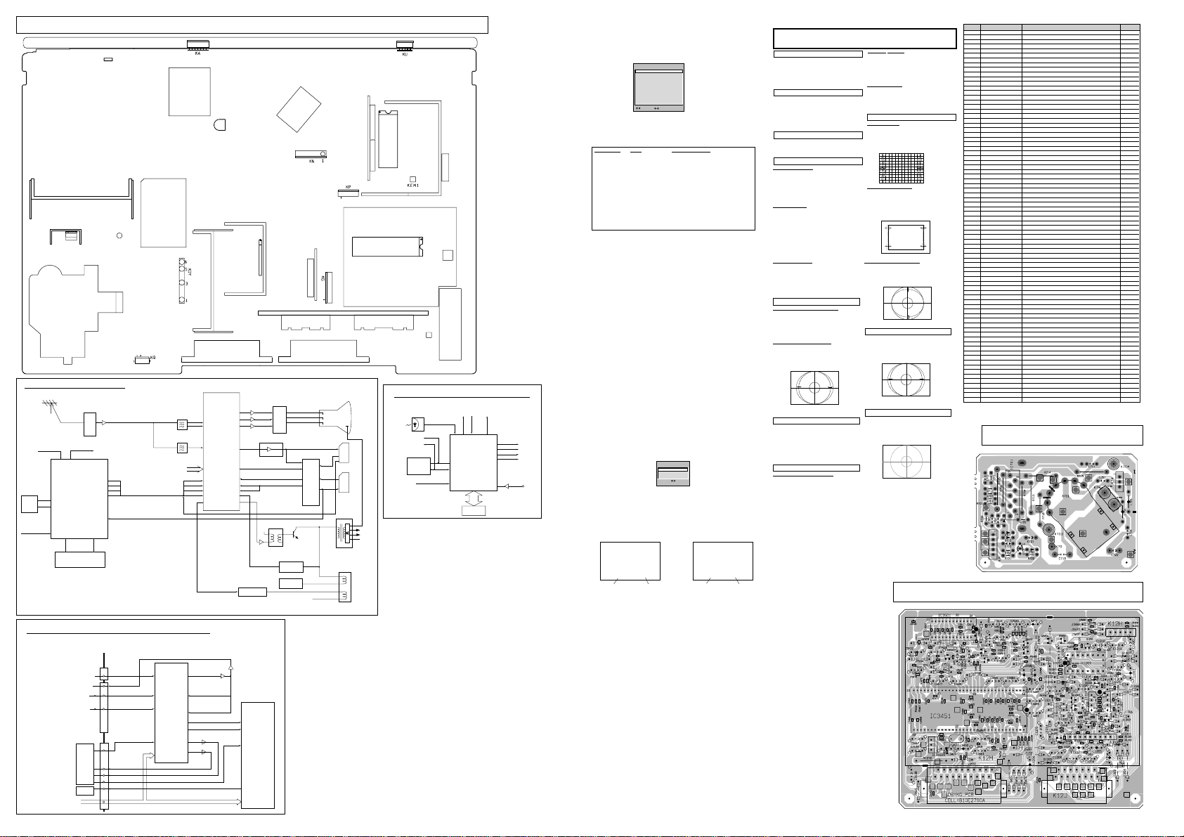
MAIN BOARD
O
ADJUSTMENTS
IMPORTANTNOTICE
Do not attempt to adjust the following service adjustments except when adjustments are required in servicing
otherwise it may cause loss of performance and product safety.
1.Receive white raster pattern.
2.Set controls to normal.
3.Connect digital voltmetre to test point TP-B and GND.
4.Adjust voltage to 130 ±0.5V using VR641 (21" model).
Adjust voltage to 150
±0.5V using VR641 (25" model).
Adjust voltage to 150 ±0.5V using VR641 (28" model).
1.Input and tune a VHF RF signal which has the
strongest signal strength.
2.Connect digital voltmetre to test point TP-A and GND.
4.Enter to the ser vice mode and select mode “REGULAR”, and select item no.1 “REGULAR 1, AGC”.
5.Press the
LEVEL+ or LEVEL - button to adjust voltage
to be 3.2Vdc.
By using FOCUS VR, adjust focus control for well
defined scanning lines.
SCREEN
ADJUSTMENT
1.Receive black & white pattern.
2.Enter to the ser vice mode and select mode “REGULAR”, and select item no.2 “REGULAR 2, CUT”. The
horizontal line will appear on the screen.
3.Set the SCREEN VR for one colour to be just visible.
4.Using the numeric buttons shown set each colour to
minimum by decreasing to the point where any further
decrease resets the adjustment to maximum value.
BIAS
ADJUSTMENT
5.By using the buttons 1, 2, 4, 5, 7, 8 on the remote
control, adjust the line to be white.
The key allocation is as follows;
Bu
tton No. Operation
1 Increase Red
2 Decrease Red
4 Increase Green
5 Decrease Green
7 Increase Blue
8 Decrease Blue
DRIVE
ADJUSTMENT
6.Select item no.3 “REGULAR 3, GRY” (G-Drive) or 4
“REGULAR 4, GRY”(B-Drive) and adjust both initially
to 3F.
7.Change data value of each item by using LEVEL + or
LEVEL - button to obtain the proper white balance.
PCC ADJUSTMENT
1.Receive cross hatch pattern and set screen mode to
“FULL”.
2.Enter to the ser vice mode and select mode “WIDE”,
and select item no.7 “WIDE 7.P PCC”.
3.Press the LEVEL+ or LEVEL - button to adjust the
vertical line to be straight.
TRAPEZOID ADJUSTMENT
1.Receive cross hatch pattern and set screen mode to
“FULL”.
2.Enter to the ser vice mode and select mode “WIDE”,
and select item no.8 “WIDE 8.P TRP”.
3.Press the LEVEL+ or LEVEL - button to correct the
trapezum distortion of the vertical line.
PCC ADJUSTMENT
GREY SCALE ADJUSTMENT
FOCUS ADJUSTMENT
AGC ADJUSTMENT
+ B VOLTAGE ADJUSTMENT
CORNER ADJUSTMENT
1.Tune the receiver to a cross hatch pattern.
2.Enter to the ser vice mode and select mode “WIDE”,
and select item no.10 “WIDE 10.P CNR”.
3.Press the
LEVEL+ or LEVEL - button to correct the
distortion of the vertical line around the corners.
HORIZONT
AL CENTRING ADJUSTMENT
1.Tune the receiver to a circular pattern.
2.Enter to the ser vice mode and select mode “WIDE”,
and select item no.2 “WIDE 2.P H-P”.
3.Press the
LEVEL+ or LEVEL - button to adjust the
horizontal centre.
HORIZONT
AL WIDTH ADJUSTMENT
1.Tune the receiver to a circular pattern.
2.Enter to the ser vice mode and select mode “WIDE”,
and select item 6 “WIDE 6.P H-W”.
3.Press the
LEVEL+ or LEVEL - button to adjust the
horizontal width.
1.Tune the receiv er to a circular pattern.
2.Set controls to normal.
3.Connect high-voltage meter to the anode of CRT and
GND.
4.Confir m that voltage is 38.0±1.0kV for 21” model.
Confirm that voltage is 29.0±1.0kV for 25”model.
Confirm that voltage is 29.0±1.0kV for 28”model.
VER
TICAL CENTRING ADJUSTMENT
1.Tune the receiver to a circular pattern.
2.Enter to the ser vice mode and select mode “WIDE”,
and select item no.1 “WIDE 1.P V-P”.
.3 Press the LEVEL+ or LEVEL - button to adjust the
vertical centre.
VER
TICAL HEIGHT ADJUSTMENT
1.Tune the receiver to a circular pattern.
2.Enter to the ser vice mode and select mode “WIDE”,
and select item no.5 “WIDE 5.P V-S.
3.Press the
LEVEL+ or LEVEL - button to adjust the
vertical height.
1.Tune the receiver to a circular pattern.
2.Enter to the ser vice mode and select mode “REGULAR”, and select item no.7 “REGULAR 7.HBF”.
3.Press the LEVEL+ or LEVEL - button to adjust the
centre of picture image to be screen centre.
1.Tune the receiver to a circular pattern.
2.Enter to the ser vice mode and select mode “REGULAR”, and select item no.8 “REGULAR 8 OSD”. The
OSD test bar will appear on the top of screen.
3.Press the LEVEL+ or LEVEL - button to adjust proper
OSD positioning.
OSD POSITIONING ADJUSTMENT
H-BLANK ADJUSTMENT
VERTICAL ADJUSTMENT
HIGH-VOLTAGE CONFIRMATION
HORIZONTAL ADJUSTMENT
T611
Q613
Q461
BLOCK DIAGRAM (OUTLINE)
Aerial
PC-IN
POWER
26
25
IC801
SCL
24
IC803
MEMORY
PROTECT-IN
BLOCK DIAGRAM (AV SELECTOR/ NICAM DECODER)
FIG. 2
Part No. SKP20350 C2WYV (SHEET 3-3)
CPU
SDA
23
1 - 15
19
80 - 63
IC802
ROM
FRONT-AV
IF/VIDEO/
CHROMA
AUDIO-OUT
I2C BUS
TP-B
T451
A101
TUNER
Q141
BLK
44
B
45
G
46
R
47
CVBS-IN
60
61
K12H
FRONT AV3
MONITOR-OUT
SC-1
SC-2
IC201
IC001
SC-1
(VIDEO/AUDIO-L/R)
SC-2
(VIDEO/Y/C/AUDIO-L/R)
K12J
(VIDEO)
C-OUT
Y-OUT
SIF-IN
AUDIO L/R-OUT
AV-SELECTOR
1(V)
2(L)
4(R)
13(V)
14(L)
16(R)
7(V)
8(L)
9(Y)
10(R)
11(C)
41(V)
SDA/SCL
I2C BUS
IC1201
<MM1313>
PTION SETTING
[After replacing the Memory IC (IC803)]
The memory IC, IC803, stores the option data of TV set and service adjustments data for each circuit, therefore,
when the memory IC is replaced, it should be performed following setting and SERVICE ADJUSTMENT on next
page.
To enter to the Option Mode
+ Press and hold the F/OK button on the remote control and P▼button on the front panel of the TV.The option win-
dow will appear on the screen. Enter the settings as shown below for the correct SERVICE REF. NO..
KMA
T681
VR641
IC501H2
IC801
UNDERSIDE OF BOARD
IC501
IC802
KMB
IC001
IC201
KX
T131
Q432
IC501H3
A101
KJ
Q121~Q133
H-OUT
Q431
&
IC701
VIDEO-OUT
R
G
B
T431
3
K1001
R
G
B
TV-IN
SIF-IN
C-OUT
Y-OUT
Refer also
to FIG.-2.
AV SELECTOR
NICAM DECODER
Q432
PCC
CONTROL
CS
CONTROL
13
8
15
18
K1002
Q242
L-OUT
R-OUT
Y-IN
C-IN
6
7
9
IF/VIDEO/
CHROMA/
34
35
15
16
17
18
26
Q1204/1207
Q1205
IC201
DEF
Q1202
AUDIO-OUT
20
21
22
54
3
43
39
40
41
32
V-OUT IC501
6
Q1203
37
36
STEREO
<TDA9875>
12
60
61
4
5
Q243
Q244
C
Y
SYNC-IN
EW-OUT
IC3451
NICAM
X132
VIF
X131
SIF
BLK
R
G
B
MONITOR-OUT
(V)34
31
29
33
32
Y-OUT
37
C-OUT
38
TV-OUT
SC-1
SC-2
MONTO
-OUT
KM
CRT
AV1
AV2
T451
FBT
FOCUS
SCREEN
D.Y
V
H
TP-A
BLOCK DIAGRAM (SYSTEM CONTROL)
RC-IN
KEY-IN
MUTE
POWER
25 26 28
40
44
45
46
IC801
47
24
CPU
23
19
60
1 - 7, 63 - 80
61
IC802
ROM
FIG. 3
I2C BUS
CONTROL
IC803
MEMORY
POWER-FAIL
DETECT
SCL
SDA
BLK-OUT
B-OUT
G-OUT
R-OUT
CVBS
Q806
To set the option mode
+ Highlight the desired option item by using the P▲ or P▼ button .
+ To switch the option mode, use the Volume - (LEFT) or Volume + (RIGHT) button.
+ The data which is set in the option mode is stored into the memory IC automatically.
Following table shows the available option items and default setting mode.
Option Mode Mode Description & Note
ON-TIMER ON or OFF On-timer available, default OFF
SORT MODE AUTO TUNE/SORT Tuning mode, default AUTO TUNING"
PLUG & PLAY ON or OFF Plug & Play mode, default ON
WELCOME TEXT ON or OFF Display message when first set up, default ON
CODE TEST OFF or ON For factory use, default OFF
WSS ON or OFF Wide Screen Signaling available, default ON
WIDE ON or OFF Wide mode, default ON
OPTION 4 LANGUAGE
312/313 Mode ON or OFF Teletext mode, default OFF
AV3 OPTION ON or OFF Front AV disable, default ON
SIF OPTION ON or OFF Television system, default BG I L/L’
Exit from the Service Mode
+ Press the RECALL button.
SERVICE ADJUSTMENTS
Note:Some items of the ser vice adjustments for this chassis are controlled by the CPU, IC801, and the
adjustments are carried out by using the RC handset.
[After replacing the Memory IC (IC803)]
The memory IC, IC803, stores the service adjustments data for each circuit, therefore, when the memory IC is
replaced, it should be performed “OPTIONSETTING” on previous page and the following adjustments, refer to
further adjustment on page 14.
ADJUSTABLESERVICE ADJUSTMENT
REGULAR
Item No. OSD Description
1 AGC AGCAdjustment
2 CUT Cut-Off Drive Adjustment
3 GRY G-Drive Adjustment
4 GRY B-Drive Adjustment
7 HBP H-Blanking Phase Adjustment
8 OSD OSD Positioning Adjustment
WIDE
Item No. OSD Description
1 P V-P Vertical Centre Adjustment
2 P H-P Horizontal Centre Adjustment
5 P V-S Vertical Size Adjustment
6 P H-S Horizontal Size Adjustment
7 P PCC Pcc Adjustment
8 P TRP Trapezoid Distortion Adjustment
10 P CNR Corner Adjustment
IMPORTANTNOTICE
Do not attempt to adjust service adjustments not listed on the above otherwise it may cause
loss of performance and product safety.
To enter to the Service Mode
+ Press and hold the GREEN button on the remote control and then press the P▼button inside of the door. The
adjustment window will appear on the screen.
To select the mode and service item and change data value
+ Highlight the desired adjustment mode by using the P▲ or P▼ button and then press the F/OK button.
+ To select the adjustment item, use the P▲or P▼ button.
+ To change the service data, use the Volume -(LEFT) or Volume + (RIGHT) button.
+ The data which is set in the service mode is stored into the memory IC automatically.
Adjustment No.
and Item name
Exit from the Service Mode
+ Press the RECALL button or turn off the TV set by using the Mains switch.
INITIALISATION OFMEMORY IC
To initialise the memory IC (IC803), press and hold the NORMALbutton on te remote control and then press the P▲
button on the front panel of the TV set, and then turn the Mains switch Off and On.Now the initialisation is
completed.
When initialised the memory IC, all of the setting data (option data and service adjustment data) stored in the IC are
reset to the default value.So it is necessary to set the option settings and readjust the service adjustments listed on
left page.
or AUTO TUNING
or ATS EUROPLUS
or ALL LANGUAGE
REGULAR mode
REGULAR
1, AGC 38
OPTION
ON-TIMER ON
SORT MODE
AUTO TUNING
PLUG & PLAY
WELCOME TEXT
CODE TEST
WSS
WIDE
OPTION
312/313 Mode
AV3 OPTION
3D SURROUND
SIF OPTION
AUTO VOLUME
ADJUST : EXIT : RECALL
REGULAR
WIDE
OTHERS
TB1251
SELECT:
EXIT : RECALL
Adjustment Data
ON
SERVICE REF. NO. CE28DN6-C-00
ON
CE25DN6-C-00
OFF
ON
CE21DN6-C-00
OFF
4 LANGUAGE
ON
ON
ON
BG & DK
OFF
Destination option , default 4 LANGUAGE
ADJUST
OK
Adjustment No.
and Item name
WIDE mode
WIDE
1. P V-P 1F
Adjustment Data
❚❚❚❚❚❚❚❚❚❚❚❚❚❚❚❚❚❚❚❚
A2 STEREO BOARD
CPU PORT FUNCTIONS
Pin No. Function Name Function IN/OUT
1 MMU0 External memory 0 OUT
2 MMU3 External memory 3 OUT
3 ADDR10 Address bus 10 OUT
4 DSN Data Strobe
5 ADDR11 Address bus 11 OUT
6 ADDR9 Address bus 9 OUT
7 ADDR8 Address bus 8 OUT
8 R WN Read Write Strobe
9 GND
10 VDD Power Supply IN
11 OSC-IN Clock Input IN
12 OSC-OUT Clock Output OUT
13 ADDR13 Address bus 13 OUT
14 ADDR14 Address bus 14 OUT
15 MMU1 External memory 1 OUT
16 MMU2 External memory 2 OUT
17 MMU4 External memory 4 OUT
18 MMU5 External memory 5 OUT
19 P3.7/CSO Protect - Power failure detect input IN
20 P3.6/ASN Dolby CLK(L/L’) OUT
21 P3.5 Dolby SO(Super 3D) OUT
22 P3.4 PITTARI switch OUT
23 P5.1 IIC BUS SDA IN/OUT
24 P5.0 IIC BUS SCL OUT
25 P2.0 Remote Control Signal Input IN
26 P2.3 Power Relay & LED Drive On:L OUT
27 P2.4 SUB CPU SO OUT
28 P0.2 Key switch input IN
29 P0.1 SUB CPU CLK OUT
30 P0.0 SUB CPU SI IN
31 P4.7 THRESHOLD switch OUT
32 P4.6 JIMAKU(Caption) switch OUT
33 P4.5 On-Timer LED Drive ON: L OUT
34 VDD IN
35 GND
36 P2.1 AV1 Scart function input IN
37 P2.2 AV2 Scart function input IN
38 P2.5 RF AGC input IN
39 P4.4 H-Blank On/Off OUT
40 P4.3 AMP Mute Mute On: H OUT
41 P4.2 Dolby RQ OUT
42 P4.1 H-Blank Phase OUT
43 P4.0 50/60Hz output 50Hz: H OUT
44 FB BLKOutput for OSD (Active H) OUT
45 B Blue Output for OSD (Active H) OUT
46 G Green Output for OSD (Active H) OUT
47 R Red Output for OSD (Active H) OUT
48 V-SYNC V-Sync Input (Active H) IN
49 H-SYNC H-Sync Input (Active H) IN
50 WSCR VPS/WSS Slicer Line PLL
51 WSCF VPS/WSS Slicer Line PLL
52 VDD-A Analogue P
53 PXFM Pixel Frequency Multiplier
54 RESET Reset Input (Active L) IN
55 MCFM Pixel Frequency Multiplier
56 JTRSTO
57 TXCF
58 CVBS0
59 TEST0
60 CVBS1
61 CVBS2 Video Signal Input IN
62 GND-A
63 DAT3 Data bus 3 IN
64 DAT4 Data bus 4 IN
65 DAT5 Data bus 5 IN
66 DAT6 Data bus 6 IN
67 DAT7 Data bus 7 IN
68 DAT2 Data bus 2 IN
69 DAT1 Data bus 1 IN
70 DAT0 Data bus 0 IN
71 ADDR0 Address bus 0 OUT
72 ADDR1 Address bus 1 OUT
73 ADDR2 Address bus 2 OUT
74 ADDR3 Address bus 3 OUT
75 ADDR4 Address bus 4 OUT
76 ADDR5 Address bus 5 OUT
77 ADDR6 Address bus 6 OUT
78 ADDR7 Address bus 7 OUT
ADDR12 Address bus 12 OUT
79
ADDR15 Address bus 15 OUT
80
ower Supply
Video signal Input IN
CRT BOARD
IN
 Loading...