

Page 1
Part No. SKSM0794 C7VDS MARCH 2005
Colour Television
Service Manual
Model CE28DFN3-B
Service Ref. No. CE28DFN3-B-00
PRODUCT CODE: 111361003
ORIGINAL VERSION: Chassis No. EB8-D
Give complete "SERVICE REF. NO." for parts
order or servicing, it is shown on the rating sheet
on the cabinet back of the TV set.
Note
This TV receiver will not work properly in foreign
countries where the television transmission
system and power source differ from the design
specifications. Refer to the specifications for the
design specifications
CE28DFN3-B
Contents
Safety precautions/Specifications ..................................................................................................................2
Block diagrams ..............................................................................................................................................3
Cabinet Disassembly......................................................................................................................................4
Adjustment and Repair Procedures............................................................................................................5~9
CPU Functions ..............................................................................................................................................................................10~1 1
Component Locations ..................................................................................................................................12
IC Block Diagrams..................................................................................................................................13~15
Pin description of semiconductors................................................................................................................16
Part Description and reading of schematic diagram ....................................................................................17
Cabinet Parts List ........................................................................................................................................18
Electric Parts List....................................................................................................................................19~24
Please use Schematic Diagram SKP20528
with this Service Manual.
+
-
Page 2

-2-
C7VDS
SAFETY PRECAUTION
X-RADIATION PRECAUTION
The primary source of X-RADIATION in the television receiver is the picture tube. The picture tube is specially
constructed to limit X-RADIATION emissions. For continued X-RADIATION protection, the replacement tube
must be the same type as the original including suffix letter. Excessive high voltage may produce potentially
hazardous X-RADIATION. To avoid such hazards, the high voltage must be maintained within specified limit.
Refer to this service manual, high voltage adjustment for specific high voltage limit. If high voltage exceeds
specified limits, take necessary corrective action. Carefully follow the instructions for +B1 volt power supply
adjustment, and high voltage adjustment to maintain the high voltage within the specified limits.
PRODUCT SAFETY NOTICE
SPECIFICATIONS
Product safety should be considered when a component replacement is made in any area of a receiver.
Components indicated by mark in the parts list and the schematic diagram designate components in which
safety can be of special significance. It is particularly recommended that only parts designated on the parts list in
this manual be used for component replacement designated by mark . No deviations from resistance wattage
or voltage ratings may be made for replacement items designated by mark .
1: An isolation transformer should be connected in the
power line between the receiver and the AC line
when a service is performed on the primary of the
converter transformer of the set.
2: Comply with all caution and safety-related notes
provided on the cabinet back, inside the cabinet, on
the chassis or the picture tube.
3: When replacing a chassis in the cabinet, always be
certain that all the protective devices are installed
properly, such as, control knobs, adjustment covers
or shields, barriers, isolation resistor-capacitor networks
etc. Before returning any television to the customer,
the service technician must be sure that it is completely
safe to operate without danger of electrical shock.
Power source AC 220~240V, 50Hz
Television system System I
Colour system PAL/NTSC4.43 (PAL/NTSC4.43/NTSC3.58 IN AV MODE)
Receiving channel UHF: #21~69
Aerial input impedance 75ohm
Rear AV terminal
AV1: CENELEC standard
INPUT: Composite video, RGB and Audio L/R
OUTPUT: TV-output with composite video and audio L/R
AV2: CENELEC standard
INPUT: Composite video, RGB, S-VHS and Audio L/R
OUTPUT: Monitor output with composite video and Audio L/R
Front AVterminal
AV3: RCA jacks
INPUT: Composite video and Audio L/R
Sound output(Music) 12 x 2
Dimensions (WxHxD) 786 x 519 x 500mm
Weight 34.8 Kg
!
!
!
Page 3
-3-
C7VDS
BLOCK DIAGRAM
This is a diagram for all models and therefore differs slightly from the actual block diagram.
AV3 H/P
Outline
CI SLOT
1AV4U20B64200
DIGITAL
SPK - L
PL8004
PL8003
PL8002A PL8006
PL8002B
PL8005
TUNER
K2 - 6V SUPPLY - PL8004
K4 - COMM - PL8002A
K16F
1AA0B10E689AA 1AA0B10E689AB
K2
KH
KA
1AA0B10H068PA K5
MAIN UNIT DIGITAL MODULE
A101
K4
K9
K4A KP
K3
K4B
KQ
K16E - DEGAUSSING
K4B (VERTICAL) RF IN
PWB SOCKET
1AA0B10H068PB
K4A (HORIZONTAL)
K16E
FRONT UNIT A FRONT UNIT B
ON/OFF
K19H SPK - R
K16FF K1103
KF
240VAC
K7P K3 - AUDIO - PL8003
KQ K7Q K9 - VIDEO - PL8002B
KP K7P K5 - GND - PL8005
K7Q
Page 4
-4-
C7VDS
(A)
(A)
CABINET DISASSEMBLY
CABINET BACK DISASSEMBLY
1. Remove 9 screws(A) for 28”
2. Pull out the cabinet back.
(A)
(A)
(A)
(A)
(A)
(A)
(A)
Page 5
-5-
C7VDS
OPTION SETTING
[After replacing the Memory IC (IC801)]
The memory IC, IC801, stores the option data of TV set and service adjustments data for each circuit, therefore,
when the memory IC is replaced, it should be programmed to the following settings and “SERVICE ADJUSTMENT”
on pages 6 to 9.
To enter to the Option Mode
+ Press and hold the F/OK button on the remote control and P▼ button on the front panel of the TV. The option
window will appear on the screen.
To set the Option Mode
+ Highlight the desired option item by using the P▲ or P▼ button .
+ To switch the option mode, use the
Volume - (LEFT) or Volume + (RIGHT) button.
+ The data which is set in the option mode is stored into the memory IC automatically.
The following table shows the available option items and default setting mode.
Exit from the Service Mode
+ Press the MENU button.
Option Mode Mode Description & Note
SORT MODE SORTING or Tuning mode, default “SORTING”
TUNING
PLUG & PLAY ON or OFF Plug & Play mode, default “ON”
WELCOME TEXT ON or OFF Display message when first set up, default “ON”
AUTO VOLUME ON or OFF Auto volume default “OFF”
SURROUND ON or OFF Surround sound default “ON”
VIRT SUB WOOFER ON or OFF Virtual Sub Woofer default “ON”
WIDE ON or OFF Wide mode, default “ON”
AV3 ON or OFF Front AV disable, default “ON”
OPTION MODE FOR CE28DFN3-B-00
i
OPTION
SORT MODE SORTING
PLUG & PLAY ON
WELCOME TEXT ON
AUT O VOLUME OFF
SURROUND ON
VIRT SUB WOOFER ON
WIDE ON
AV3 ON
ADJUST : EXIT : RECALL
Page 6
-6-
C7VDS
SERVICE ADJUSTMENTS
After replacing the Memory IC (IC801)]
The memory IC, IC801, stores the service adjustments data for each circuit, therefore, when the memory IC is
replaced, it should be programmed by using “OPTION SETTING” on previous page and the following adjustments.
ADJUSTABLE SERVICE ADJUSTMENT
Item No. OSD Description
6 Screen adjustment
151 WPR - N R - Drive adjustment
152 WPG - N G - Drive adjustment
304 AGC Take Over AGC adjustment
314 TXT - H - POS OSD Positioning adustment
IMPORTANT NOTICE
Do not attempt to adjust service adjustments not listed above otherwise it may cause loss of performance and product safety.
GEOMETRY SERVICE DATA
Service Item Number. Symbol 1 Symbol 2
13
14 A02
15 A03
16 A04
17 A05
18 A06
19 A07
20 A08
21 A09
22 A10
23 A11
24 A12
25 A13
26 A14
27 A15
28 A16
29 A17
30 A18 H BLK SW
31 A19 H BLK L
32 A20 H BLK R
33 A21 OSVE
34 A22 EVB
35 B02
36 B09
37 B10
38 B11
39 B12
40 B13
41 B14
42 B15
43 B16
44 B17
A01
Track. mode 50Hz Full
Vert. Zoom 50Hz Full
Vert. Slope 50Hz Full
Vert. Shift 50Hz Full
Vert. Ampl. 50Hz Full
S-Corr. 50Hz Full
V.Lin.Ctrl. 50Hz Full
V.Linearity 50Hz Full
EW Width 50Hz Full
Hor. Shift 50Hz Full
EW Parabola 50Hz Full
Trapezium 50Hz Full
UC Parabola 50Hz Full
LC Parabola 50Hz Full
Hor. Bow 50Hz Full
Parallel 50Hz Full
Vert. Scroll 50Hz Full
Vert. Zoom 50Hz Natural / or 4:3 squeeze mode
EW Width 50Hz Natural / or 4:3 squeeze mode
Hor. Shift 50Hz Natural / or 4:3 squeeze mode
EW Parabola 50Hz Natural / or 4:3 squeeze mode
Trapezium 50Hz Natural / or 4:3 squeeze mode
UC Parabola 50Hz Natural / or 4:3 squeeze mode
LC Parabola 50Hz Natural / or 4:3 squeeze mode
Hor. Bow 50Hz Natural / or 4:3 squeeze mode
Parallel 50Hz Natural / or 4:3 squeeze mode
Vert. Scroll 50Hz Natural / or 4:3 squeeze mode
Frequency Wide Mode
50Hz Full
50Hz Full
50Hz Full
50Hz Full
50Hz Full
Explanation
Track. Mode(HCO)
Vertical zoom
Vertical slope
Vertical shift
Vertical amplitude
S-correction
V.Lin.Ctrl.
V.Linearity
EW width
Horizontal shift
EW parabola/width
EW trapezium
EW upper corner parabola
EW lower corner parabola
Horizontal bow
Horizontal parallelogram
Vertical Scroll
RGB blanking mode
Timing of wide blanking front(WBF)
Timing of wide blanking rear(WBR)
Black current measuring lines in overscan
Extended vertical blanking
Vertical zoom
EW width
Horizontal shift
EW parabola/width
EW trapezium
EW upper corner parabola
EW lower corner parabola
Horizontal bow
Horizontal parallelogram
Vertical Scroll
Page 7
-7-
C7VDS
To enter to the Service Mode
+ Press and hold the GREEN button on the remote control and then press the P▼ button on the cabinet.
To select the service item and change data value
+ To select the adjustment item, use the P▲ or P▼ button.
+ To change the service data, use the Volume -(LEFT) or Volume + (RIGHT) button.
+ The data which is set in the service mode is stored into the memory IC automatically.
SERVICE MODE
SERVICE SERVICE SOFTWARE
ITEM ITEM VERSION
NUMBER DESCRIPTION
Exit from the Service Mode
+ Press the MENU button or turn off the TV set by using the Mains switch.
INITIALISATION OF MEMORY IC
To initialise the memory IC (IC801), press and hold the NORMAL button on the remote control, then press
the P▼ button on the front panel of the TV set. The tv set will switch into standby mode. Turn the Mains switch Off
and On, then switch on from standby. The initialisation is now completed.
When initialised the memory IC and all of the setting data (option data and service adjustment data) stored in the IC
are reset to the default value. It is necessary to set the option settings and readjust the service adjustments listed in
this manual and to re-tune all the channels.
SERVICE
000 EB8D 3_52
i
Page 8
-8-
C7VDS
ADJUSTMENTS
IMPORTANT NOTICE
Do not attempt to adjust the following service adjustments except when adjustments are required in servicing
otherwise it may cause loss of performance and product safety.
1. Receive white raster pattern.
2. Set controls to normal.
3. Connect digital voltmetre to test point TP-B and GND.
4. Adjust voltage to 150 ±0.5V by using VR641.
1. Input and tune an RF signal which is UHF to the clearest station.
2. Connect digital voltmetre to test point TP-A and GND.
4. Enter the service mode and select item no. 304. AGC
TAKE OVER
5. Press the LEVEL+ or LEVEL - button to adjust volt-
age to be 3.2Vdc.
By using FOCUS VR, adjust focus control for well
defined scanning lines.
SCREEN ADJUSTMENT
1. Enter the service mode and select item no. 6.
COLLAPSED LINE
2. Turn screen VR until collapsed line is just visible then
stop turning. Press menu key on remote control to exit
the service mode.
DRIVE ADJUSTMENT
3. Select item no.151. WPR - N (R-Drive) or 152. WPG -
N (G-Drive) and adjust both initially to 20.
4. Change data value of each item by using LEVEL + or
LEVEL - button to obtain the proper white balance.
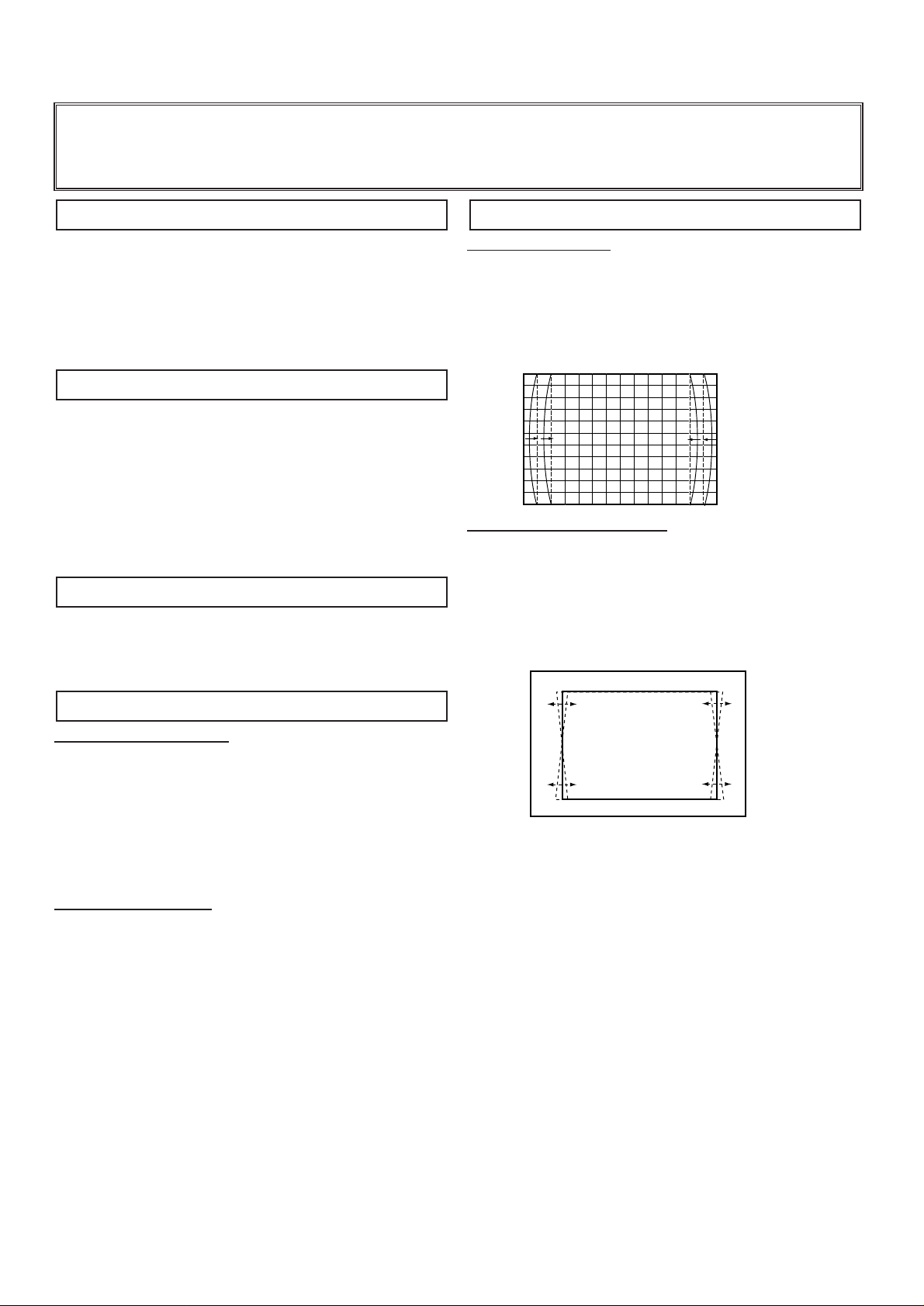
PCC ADJUSTMENT
1. Receive cross hatch pattern and set screen mode to
“FULL”.
2. Enter the service mode and select item no. 23. EW
PARABOLA
3. Press the LEVEL+ or LEVEL - button to adjust the
vertical line to be straight.
TRAPEZOID ADJUSTMENT
1. Receive cross hatch pattern and set screen mode to
“FULL”.
2. Enter the service mode and select item no. 24.
TRAPEZIUM
3. Press the LEVEL+ or LEVEL - button to correct the
trapezum distortion of the vertical line.
PCC ADJUSTMENT
GREY SCALE ADJUSTMENT
FOCUS ADJUSTMENT
AGC ADJUSTMENT
+ B VOLTAGE ADJUSTMENT
Page 9
-9-
C7VDS
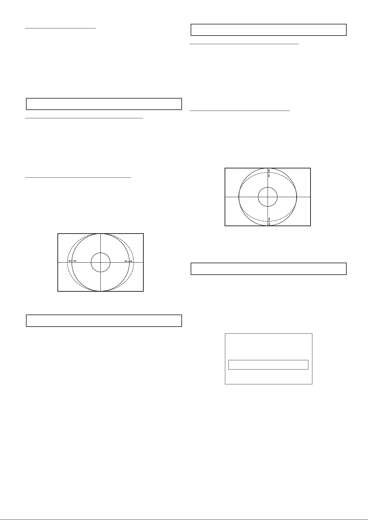
CORNER ADJUSTMENT
1. Receive cross hatch pattern and set screen mode to
“FULL”.
2. Enter the service mode and select item no. 25. UC
PARABOLA for top corner adjustment OR item no.
26. LC PARABOLA for bottom corner adjustment.
3. Press the LEVEL+ or LEVEL - button to correct the
distortion of the vertical line around the corners.
HORIZONTAL CENTRING ADJUSTMENT
1. Receive circular pattern and set screen mode to
“FULL”.
2. Enter the service mode and select item no. 22. HOR.
SHIFT.
3. Press the LEVEL+ or LEVEL - button to adjust the
horizontal centre.
HORIZONTAL WIDTH ADJUSTMENT
1. Receive circular pattern and set screen mode to
“FULL”.
2. Enter to the service mode and select item 21. EW
WIDTH.
3. Press the
LEVEL+ or LEVEL - button to adjust the
horizontal width.
1. Receive circular pattern and set screen mode to
“FULL”.
2. Set controls for brightness and contrast to maximum.
3. Connect high-voltage meter to the anode of CRT and
GND.
4. Confirm that voltage is 26 kV ±1.0kV at maximum
beam current 1.2mA ± 0.05
VERTICAL CENTRING ADJUSTMENT
1. Receive circular pattern and set screen mode to
“FULL”.
2. Enter the service mode and select item no.16.VERT
SHIFT.
.3 Press the LEVEL+ or LEVEL - button to adjust the
vertical centre.
VERTICAL HEIGHT ADJUSTMENT
1. Receive circular pattern and set screen mode to
“FULL”.
2. Enter the service mode and select item no. 17. VERT
AMPL.
3. Press the LEVEL+ or LEVEL - button to adjust the
vertical height.
1. Receive circular pattern and set screen mode to
“FULL”.
2. Enter the service mode and select item no. 314. TXT H - POS.
3. Press the
LEVEL+ or LEVEL - button to adjust
proper OSD positioning.
OSD POSITIONING ADJUSTMENT
VERTICAL ADJUSTMENT
HIGH-VOLTAGE CONFIRMATION
HORIZONTAL ADJUSTMENT
314 TXT - H - POS 7
Page 10

-10-
C7VDS
CPU PORT FUNCTIONS
Pin No Function Name Function In/Out
1 VSS Gnd -2 VSS Gnd
3 1v8_1 1.8v Supply -4 3v3 3.3v Supply -5 Vref 3.3v Reference -6 Vref V Ref Gnd -7 Vref 3.3v Reference -8 Vref V Ref Gnd --
9 Vref 3.3v Reference -10 XTAL IN Clock Oscillator In
11 XTAL OUT Clock Oscillator Out
12 Vss Gnd -13 Vguard sw -14 Dec Dig 1.8v source supply Out
15 5v 5v Supply -16 Phi 2 Phi 2 -17 Phi 1 Phi 1 -18 Gnd Gnd -19 Sec pii -20 Dec BG -21 EW Drive parabola out Out
22 VdrB Vertical drive B Out
23 VdrA Vertical drive A Out
24 Vif 1 Vision IF 1 In
25 Vif 2 Vision IF 2 In
26 Vsc -27 I Ref Reference current -28 Gnd Gnd -29 Sif 1 Sound IF 1 In
30 Sif 2 Sound IF 2 In
31 Agc Auto matic gain control In
32 Eht Eht In
33 SSif/Ref Iin/Avl/Ref Out -34 Audio in Scart L In
35 Audio in Scart R In
36 Audio Out Scart L Out
37 Audio Out Scart R Out
38 -39 Qsso/Amo/AudioEm -40 Gnd -41 PLL IF Phase Lock Loop If -42 SifAgc SifAgc -43 IFVo Scart 1 Video Out
44 FmRo -45 V8Audio Switches -46 AgcsSif -47 V5P2 5v Supply -48 Svo/IfVo/Cbvs1 Scart 2 Video Out
49 Audio4 L In Scart 2 Audio L In
50 Audio4 R In Scart 2 Audio R In
51 Y4/Cvbs4 Av3 Video In
52 C4 -53 Audio2InL Av3 Audio L In
54 Audio2InR Av3 Audio R In
55 Cvbs2/y Scart 1 Video In
56 Audio3InL -57 Audio3InR -58 Y3/Cvbs Scart 2 Video In
59 C3 Scart 2 Chroma In In
60 Audio Out L SL Audio out Left Speaker Out
61 Audio Out L SR Audio Out Right Speaker Out
62 Audio Out HPL Scart Audio L Out 2 / monitor Out Out
63 Audio Out HPR Scart Audio R Out 2 / monitor Out Out
64 Pip --
Page 11

-11-
C7VDS
CPU PORT FUNCTIONS (continued)
Pin No Function Name Function In/Out
65 SVM Scan Velocity Modulation Out
66 FbiSo Flyback In SandCastle Out In/out
67 Hout Horizontal Drive Out Out
68 VssComb Gnd
69 V5Comb 5v Supply -70 Vin/R2/Pr Scart 2 R-In In
71 Uin/B2/Pb Scart 2 B-In In
72 Yin/G2/Y Scart 2 G-In In
73 Y Sync Y Sync In
74 Y out Yout Out
75 Uout/Fb in Scart 2 Fast Blanking In
76 Vout/Sw01 -77 Fbl3 Scart 1 Fast Blanking In
78 R3/Pr Scart 1 R-In In
79 G3/Y Scart 1 G-In In
80 B3/Pb Scart 1 B-In In
81 Gnd 3 Gnd -82 V5P3 5vSupply -83 BCL Beam Current Limiting In
84 Iblack -85 Rout Red Drive Out
86 Gout Green Drive Out
87 Bout Blue Drive Out
88 V3.3A1 3.3v Supply -89 RefAdn Ref Gnd -90 V3.3RefAdp 3.3v Supply -91 RefAd -92 GndA Gnd -93 V1.8A 1.8v Supply -94 V3.3A2 3.3v Supply -95 VssAdc Gnd -96 V1.8Adc 1.8v Supply -97 Into Remote control In In
98 P10/Int1 SCl In/out
99 P121/TO SDA In/out
100 V1.8C2 1.8v Supply -101 VssC2 Gnd -102 P04/I2Sws -103 P03/I2SCLk -104 P02/I2SDOC -105 P01/I2SDOC -106 P00/I2SDi1 StandBy Out
107 P13/T1 On/Off Out
108 P16/SCL SCL In/out
109 P17/SDA SDA In/out
110 V3.3P 3.3v Supply -111 P20/Tpwm Relay On/Off Out
112 P21/Pwmo LED Drive Out
113 STATUS Status In/out
114 ALK Alk In/out
115 P30/Adco Scart 1 Pin8 Function In
116 P31/Adc1 Scart 2 Pin8 Function In
117 V1.8C1 1.8v Supply -118 DecV1v8 1.8v Supply -119 P32/Adc2 AGC In
120 P33/Adc2 Key scan in In
121 VssC1+P1 Gnd -122 P24/Pwm3 Audio Mute Out
123 P25/Pwm4 L/L’ switch (Export only) Out
124 V1.8C3 1.8v Supply -125 Vssc3 Gnd -126 P12/Int2 -127 P14/Rx Power Fail In
128 P:15/Tx Natural Wide Switch
Page 12

-12-
C5WDS
COMPONENT LOCATIONS
MAIN BOARD / CRT BOARD
KGG
12
KGG-2
KGG-1
R601
KF-1
KF
KF-2
DANGER
LIVE MAINS
E
Q462
C468
C450
D469
C451
EB8D
KH
JW3
C023
R742
K7Y
3
1
K7Q
J006
C022
KEM1
IC001
IC001
C021
JW1
E
Q204
JB
2
C009
C010
K5
E
Q202
JW2
C203
C1001
C214
X201
X122
X122A
C229
C236
C233
C239
C102
K1003
17
KCPA
C209
C103
TP-A
C104
C101
KEM2
X121
JWA
CELL=B10E00900
T131
A101
JWB
B10E0090A
DB=UK_PCB
***
D633A
D630
C502
C686
C682
D633
R667
C642
D506
R106
R502
IC501-2
D501
IC501
B10E00900
R692
C650
IC643
IC666
C685
C667
C643
D642
R501
E
E
Q651
Q642
R515
C271
K9
C1011
R699
R691
B10E0090B
C710
IC701
R725
R705
K2
K7P
1
C691
R715
K701
K7V
IC641
R644
C645
***
C648
C841
JD
C633
C803
K4
IC801
C205
8
1
4
C206
KP
K1001
C210
C288
5
C283
C281
C268
C256
K3
DIP
D1602
R1607
R602
IC1601
5
8
1
4
R1601
C1603
R1603
C609
R631
R613
R632
Q461-1
Q461
D461
C486
R486
R474
L461
R435
L441
C441
C446
KSC
R451
C614
R441
C443
C423
Q451
R443
T451
3
4
D481
R480
C445
R452
R448
T1601
D1612
C1611
3
D1601
D1603
IC601
IC601-1
1
IC1611
2
KA
R637
R648
C637
R614
R607
R606
VR641
D610
C655
D639
T611
L442
L643
D648
K4A-2
K4A-1
C421
R466
21
D441
C481
1
Q432-2
K4A
D438
C420
D439
C422
L462
KQ
3
R449
C434
C424
JW16
C466
E
JW17
Q402
TP-B
C501
C529
R512
R512A
C503
R511
R510
R433
T431
E
Q431
C511
3
K4B
C432
K1002
Page 13

-13-
C7VDS
IC BLOCK DIAGRAMS
IC001 LA42072-E <Audio Output>
IC501 LA78045 <Vertical Output>
STAND BY Vcc
5 7
INPUT AMPLIFIER
R In = 20Ko
R In = 20Ko
INPUT AMPLIFIER
MUTE
IN 2
IN 1
3
6
4
RIPPLE FILTER
1
RIPPLE FILTER
OUTPUT AMPLIFIER
Vcc GND SHORTING PROTECTION CIRCUIT.
LOAD SHORTING PROTECTION CIRCUIT
THERMAL PROTECTION CIRCUIT
OUTPUT AMPLIFIER
12
+ OUT 1
- OUT 1
11
POWER
10
GND
+ OUT 2
8
- OUT 2
9
1
INVERTING
INPUT
THERMAL PROTECTION CIRCUIT
-
AMPLIFIER
+
PUMP
UP
2
Vcc
3
OUT
4
GND
PUMP UP
5
VER
6
OUTPUT
OUTPUT STAGE Vcc
7
NON INV. INPUT
Page 14

-14-
C5WDS
IC601
Block Diagram TN6Q03/04
VDD pin
EDGE pin
FB pin
4
Internal power supply
2
Over heat protection
Over voltage protection
Reference Voltage
Over current/FB comparator
1
Input Under voltage protection
Falling edge detection
Latch
Circuit
Logic
Driver
Oscillator
Burst On
Burst Off
Latch for Burst circuit
3
DRAIN pin
5
SOURCE (GND) pin
Page 15

-15-
C7VDS
Page 16

-16-
C5WDS
PIN DESCRIPTION OF SEMICONDUCTORS
● Diode
● Transistor/FET
● IC
FET
● Diode
K
A
● Transistor/FET
K
A
K
AA
KK
A
K
K
K: Cathode
A: Anode
A
A
C
B
C
E
● IC
1
E
3
2
Index
C1
3
2
E
C2
Vdd
1
C1
C2
B1 B2
E
B2
GND
C
C
E
B
C
E
B
B
2
3
1
E
C1
CBE
C2
B2
E
3
2
C
B
B1
1
C
BE
B1
RESET
Index
1
2
N
1
2
N
C2
E2 C1
B1
B2
B1
B2
(IN)
E1
1
(GND)
2
4
5
6
Index
E1
C1
C2
E2
3
(OUT)
C: Collector
B: Base
E: Emitter
G
3
2
1
Index
D: Drain
G: Gate
S: Source
S
G
D
S
D
3
21
5
4
Index
N
1
Index
Index
Index
N
1
N
1
N
1
Index
N
1
N
1
Index
Page 17

-17-
C7VDS
PARTS DESCRIPTION AND READING IN SCHEMATIC DIAGRAM
1. The parts specification of resistors, capacitors and
coils are expressed in designated code. Please
check the parts description by the following code
table.
2. Some of transistors and diodes are indicated in
mark for the substitution of parts name. Please
check the parts name by the following code table.
3. Voltages and waveforms were taken with a video
colour bar signal(1Vp-p at 75 ohms terminated) and
controls to normal.
4. Voltages were taken with a high-impedance digital
voltmetre.
Example 2000 K K 1000 BG
Characteristic
Example 160 E M 10
Capacitance value
Tolerance
Type
Rated voltage
Excepting electric capacitors, all
capacitance values of less than 1
are expressed in µF and more
than 1 are in pF.
Example L2
C1 4R7 K N
Tolerance
Inductance value
Manufacture code
Unique code
Mark Material
E Electrolytic
P Electrolytic (non-Polarised)
C Ceramic (temperature compensation)
K Ceramic
F Polyester
N Polypropylene
M Metalised polypropylene
H Metalised polypromylar
B Ceramic (semiconductor)
G Metalised polyester
Y Composite film
S Styrol
T Tantalum oxide solid electrolytic
U Organic semiconductive electrolyte
D Electric double layer electrolytic
Mark Tolerance
A not specified
B ±0.1
C ±0.25
D ±0.5
F±1
G±2
E ±2.5
H±3
J±5
K±0
M±20
N±30
P +100 -0
Q +30 -10
T +50 -10
U +75 -10
V +20 -10
W +100 -10
X +40 -20
Y +150 -10
Z +80 -20
Mark Tolerance (nH) Mark Tolerance (%)
C ±0.25 G ±2
D ±0.5 J ±5
S ±0.3 K ±10
A ±0.2 L ±15
M±20
Coil Reading
Capacitor Reading
Example 1/2 D J 10K B
Example 6 W K 8.2
Example 1/2 C K 1M
Resistor Reading
Characteristic
Z (Carbon fuse)
B (Non-burnable)
Resistance value
Tolerance (see below table)
Material (see below table)
Rated wattage (W)
K indicates in KΩ
M indicate in MΩ
Note: Resistor which is indicated with resistance value only are
1/6W carbon resistor. Resistor which is indicated with material, tolerance and value are 1/4W rated wattage.
Mark Material
D Carbon
N Metal film
S Oxide metal film
C Solid
G Metal glaze
W Wire wounding or cement
H Ceramic
F Fusible
Mark Tolerance
A ±0.05
B ±0.1
C ±0.25
D ±0.5
F±1
G±2
J±5
K±10
M±20
P +5 -15
Z used in 0 ohm
● Material table
● Tolerance table
● Material table
● Tolerance table
Mark Type number
-- 1S1555,1S2473,1S2076,1SS133,DS442,1SS176
K 1S1555,1S2473,1S2076,DS442
L 1S1555,1S2076A,1S2471
M 1SS133,1SS176,GMA01
N 1S1555,1S2473,1S2076,1SS133,DS442,1SS176,1N4148
P 1S1555,1S2076A,1S2471,1N4148
R 1S1555,1S2076,1S2473,DS442,1N4148
AA 1S1555,1S2076,1S2473,1SS133,DS442,1SS176,1N4148,GMA01
● Diode
Mark Type number
-- 2SC536 2SC945A 2SC1815 2SC1740 2SC1740S KSC945C
A E, F, G P, Q, R O, Y, G Q, R, S Q, R, S
B E, F, G P, Q, R O, Y, G Q, R, S
D F, G P, Q Y, G Q, R, S
F F, G P G R, S
H F, G P, Q Y, G Q, R, S Y, G
I E, F, G P, Q, R O, Y, G Q, R, S Y, G
G F, G P G R, S G
AD F, G Q, R Y, GR Q, R, S
AE E, F, G Q, R O, Y, GR Q, R, S
● Transistor (NPN type)
Mark Type number
-- 2SA608 2SA564A 2SA1015 2SA933 2SA933S KSA733C
Y E, F Q, R O, Y, G Q, R
WF R Y, GR
V E, F Q, R O, Y, G Q, R Y, G
U F R Y, G R G
Z E, F Q, R O, Y, G Q, R Q, R
AB F R Y Q, R
AE E, F Q, R O, Y R
● Transistor (PNP type)
Diode/Transistor Type Reading
Page 18

-18-
C7VDS
CABINET PARTS LIST FOR MODEL CE28DFN3-B-00
CABINET PARTS
1 610 319 1287 CABINET FRONT-C7VA
2 665 000 4375 BUTTON POWER-C7VA
3 665 000 4382 BUTTON UNITED-C7VA
4 610 308 4428 CABINET BACK-C6AD
5 610 319 1331 DOOR-C7VA
6 665 000 4368 DEC IND-C7VA
7 610 253 2449 AC CORD HOLDER-U-D4VA
8 645 043 5058 BADGE,SANYO*53.5X12L53.3
ACCESSORIES
9 1AV0U10B40701 ASSY,REMOCON JXPTB
645 044 8416 BATTERY 1.5V,R03
665 000 3699 INST MANUAL - C7VD/ZD
665 000 3705 QUICK SET UP - C7VD/ZD
Item Part No. Description
Note: Parts order must contain Service Ref. No., Part No., and descriptions.
9
8
1
3
2
5
6
DS
+
-
Page 19

C7VDS
-19-
CHASSIS ELECTRICAL PARTS LIST
Product safety should be considered when a component replacement is made in any area of a receiver.
Components indicated by a mark in this parts list and the circuit diagram show components whose value have
special significance to product safety. It is particularly recommended that only parts specified on the following
parts list be used for components replacement pointed out by the mark .
013C7VDS ELECTRICAL PARTS
COIL
L901 645 068 0137 DEGAUSS 28" W/F SAMSUNG
PICTURE TUBE
Q901 414 012 9003 CRT W66QDE993X011
MISCELLANEOUS
A900 645 061 5016 UNIT,UK DIGITAL
SP901 645 047 2046 SPEAKER 8 H125/1039
SP902 645 047 2046 SPEAKER 8 H125/1039
WTU 610 309 1914 CORD,SHIELD 1L-1L,L=160,K
W901 645 011 8838 3P AC CORD +2P HOUSE @2.1
W902 610 310 7622 GND CON.EB7D 28"1220MM
1AA0B10H068RA ASSY,PWB,MAIN C7VDS
CAPACITOR
C003 403 314 5915 GRM21BR71C474KA01L PT297
C004 403 314 5915 GRM21BR71C474KA01L PT297
C005 403 215 2310 GRM188R71H123KA01D PT115
C006 403 215 2310 GRM188R71H123KA01D PT115
C011 403 269 5916 GRM219R71C224KC01D PT115
C012 403 269 5916 GRM219R71C224KC01D PT115
C013 403 269 5916 GRM219R71C224KC01D PT115
C014 403 269 5916 GRM219R71C224KC01D PT115
C015 403 269 5916 GRM219R71C224KC01D PT115
C016 403 269 5916 GRM219R71C224KC01D PT115
C017 403 269 5916 GRM219R71C224KC01D PT115
C018 403 269 5916 GRM219R71C224KC01D PT115
C021 403 047 3120 ELECT 47U M 25V
C022 403 195 8408 ELECT 2.2U M 50V
C023 403 218 8151 25 YK 1000 M TA 1020
C024 403 157 1914 GRM1885C1H100JZ01
C025 403 153 9112 GRM1885C1H5R0CD01D PT115
C026 403 068 9016 CERAMIC 100P K 50V
C040 403 113 4119 GRM188R71H222KA01D PT115
C057 403 113 3815 GRM188R71H102KA01D PT115
C1001 403 248 1618 16 YK 47 M TA 0511
C1003 403 157 3611 GRM1885C1H101JZ01D PT115
C1005 403 113 3815 GRM188R71H102KA01D PT115
C1006 403 157 3611 GRM1885C1H101JZ01D PT115
C1007 403 113 3815 GRM188R71H102KA01D PT115
C101 403 233 1111 ELECT 22U M 50V
C1011 403 248 1618 16 YK 47 M TA 0511
C1013 403 157 3611 GRM1885C1H101JZ01D PT115
C1014 403 157 3611 GRM1885C1H101JZ01D PT115
C1016 403 113 3815 GRM188R71H102KA01D PT115
C1017 403 113 3815 GRM188R71H102KA01D PT115
C102 403 039 3527 ELECT 470U M 6.3V
C1031 403 113 3815 GRM188R71H102KA01D PT115
Ref. No.
Part No.
Description
Chassis construction
CE28DFN3-B-00
013C7VDS ELECTRICAL PARTS (PAGE 19)
1AA0B10H068RA ASSY,PWB,MAIN C7VDS (PAGE 19 - 24)
1AA0B10H068RB ASSY,PWB,SOCKET C7VDS (PAGE 24)
1AA0B10E689AB ASSY,PWB,FRONT-B AV3 (PAGE 24)
1AA0B10E689AA ASSY,PWB,FRONT-A MAINS (PAGE 24)
Read description in the Capacitor and Resistor as follows:
CAPACITOR
CERAMIC 100P K 50V
Tolerance Symbols:
Less than 10PF
A: Not specified B: ±0.1PF C:±0.25PF
D: ±0.5PF F: ±1PF G: ±2PF
R: ±0.25-0PF S: ±0-0.25PF E: +0-1PF
More than 10PF
A: Not specified B: ±0.1% C:±0.25%
D: ±0.5% F: ±1% G: ±2%
H: ±3% J: ±5% K: ±10%
L: ±15% M: ±20% N: ±30%
P: +100-0% Q: +30-10% T: +50-10%
U: +75-10% V: +20-10% W:+100-10%
X: +40-20% Y: +150-10% Z: +80-20%
Material:
CERAMIC............Ceramic
MT-PAPER ..........Metallized Paper
POLYESTER ......Polyester
MT-POLYEST ......Metallized Polyester
POLYPRO............Polypropylene
MT-POLYPRO ....Metallized Polypropylene
COMPO FILM......Composite film
MT-COMPO ........Metallized Composite
STYRENE............Styrene
TA-SOLID............Tantalum Solid
AL-SOLID............Aluminium Solid
ELECT ................Electrolytic
NP-ELECT ..........Non-polarised Electrolytic
OS-SOLID ..........Aluminium Solid with Organic Semiconductive Electrolytic
DL-ELECT ..........Double Layered Electrolytic
RESISTOR
CARBON 4.7K J A 1/4W
Rated Wattage
Performance Symbols:
A: General B: Non flammable Z: Low noise
Other: Temperature coefficient
Tolerance Symbols:
A: ±0.05% B: ±0.1% C:±0.25% D: ±0.5%
F: ±1% G:±2% J: ±5% K: ±10%
M:±20% P: +5-15%
Rated value, ohms:
K: 1,000, M: 1,000,000
Material:
CARBON ............Carbon
MT-FILM..............Metal Film
OXIDE-MT ..........Oxide Metal Film
SOLID..................Composition
MT-GLAZE ..........Metal Glaze
WIRE WOUND ....Wire Wound
CERAMIC RES....Ceramic
FUSIBLE RES ....Fusible
Rated Voltage
Rated value: P=pico farad, U=Micro farad
Note: Parts order must contain Service Ref. No., Part No., and descriptions.
!
!
!
!
!
!
!
Page 20

-20-
C7VDS
Part No.
Ref. No.
Part No.
Description
Ref. No.
Description
C1033 403 113 3815 GRM188R71H102KA01D PT115
C1036 403 323 8815 GRM21BF51C225ZA01K PT115
C1037 403 323 8815 GRM21BF51C225ZA01K PT115
C1038 403 323 8815 GRM21BF51C225ZA01K PT115
C1039 403 323 8815 GRM21BF51C225ZA01K PT115
C104 403 233 0817 ELECT 10U M 50V
C1054 403 113 3815 GRM188R71H102KA01D PT115
C1055 403 113 3815 GRM188R71H102KA01D PT115
C106 403 215 2211 GRM188R71H103KA01D PT115
C107 403 215 2211 GRM188R71H103KA01D PT115
C109 403 113 3815 GRM188R71H102KA01D PT115
C110 403 113 3815 GRM188R71H102KA01D PT115
C121 403 067 6274 POLYESTER 0.15U J 50V
C122 403 215 2211 GRM188R71H103KA01D PT115
C123 403 113 3815 GRM188R71H102KA01D PT115
C126 401 105 7919 MT-GLAZE 0.000 ZA 1/16W
C1601 403 279 4807 CERAMIC 100P K 2K
C1602 403 073 6413 CERAMIC 470P K 50V
C1603 403 051 0627 ELECT 4.7U M 50V
C1605 403 16 88701 MT-POLYEST 0.022U K 400V
C1607 403 075 9719 CERAMIC 1800P K 500V
C1611 403 194 3800 ELECT 2200U M 25V
C1613 403 073 8318 CERAMIC 4700P K 50V
C200 403 215 2211 GRM188R71H103KA01D PT115
C201 403 269 5916 GRM219R71C224KC01D PT115
C202 403 269 5916 GRM219R71C224KC01D PT115
C203 403 038 3409 ELECT 1000U M 6.3V
C204 403 164 0214 GRM188F51E104ZA01D PT115
C205 403 241 3817 10 YK 220 M TA 0511
C206 403 241 3817 10 YK 220 M TA 0511
C207 403 269 5916 GRM219R71C224KC01D PT115
C208 403 323 8815 GRM21BF51C225ZA01K PT115
C209 403 195 8824 ELECT 100U M 16V
C210 403 241 3817 10 YK 220 M TA 0511
C211 403 164 0214 GRM188F51E104ZA01D PT115
C212 403 215 2211 GRM188R71H103KA01D PT115
C213 403 157 7312 GRM188R71H682KA01D PT115
C214 403 248 1410 50 YK 1R0 M TA 0511
C216 403 269 5916 GRM219R71C224KC01D PT115
C217 403 284 4314 CERAMIC 0.022U K 50V
C218 403 323 8815 GRM21BF51C225ZA01K PT115
C219 403 113 3815 GRM188R71H102KA01D PT115
C221 403 113 3815 GRM188R71H102KA01D PT115
C222 403 323 8815 GRM21BF51C225ZA01K PT115
C223 403 314 5915 GRM21BR71C474KA01L PT297
C224 403 314 5915 GRM21BR71C474KA01L PT297
C225 403 314 5915 GRM21BR71C474KA01L PT297
C226 403 323 8815 GRM21BF51C225ZA01K PT115
C227 403 323 8815 GRM21BF51C225ZA01K PT115
C228 403 164 0214 GRM188F51E104ZA01D PT115
C229 403 233 0817 ELECT 10U M 50V
C231 403 155 2210 GRM188R71H332KA01D PT115
C232 403 164 0214 GRM188F51E104ZA01D PT115
C233 403 248 2813 50 YK 2R2 M TA 0511
C234 403 164 0214 GRM188F51E104ZA01D PT115
C235 403 157 3611 GRM1885C1H101JZ01D PT115
C236 403 233 0817 ELECT 10U M 50V
C237 403 323 8815 GRM21BF51C225ZA01K PT115
C238 403 164 0214 GRM188F51E104ZA01D PT115
C239 403 233 0817 ELECT 10U M 50V
C240 403 157 3611 GRM1885C1H101JZ01D PT115
C241 403 314 5915 GRM21BR71C474KA01L PT297
C242 403 314 5915 GRM21BR71C474KA01L PT297
C243 403 164 0214 GRM188F51E104ZA01D PT115
C244 403 314 5915 GRM21BR71C474KA01L PT297
C245 403 157 3611 GRM1885C1H101JZ01D PT115
C246 403 314 5915 GRM21BR71C474KA01L PT297
C247 403 323 8815 GRM21BF51C225ZA01K PT115
C248 403 314 5915 GRM21BR71C474KA01L PT297
C249 403 314 5915 GRM21BR71C474KA01L PT297
C251 403 323 8815 GRM21BF51C225ZA01K PT115
C252 403 215 2211 GRM188R71H103KA01D PT115
C256 403 233 0817 ELECT 10U M 50V
C257 403 164 0214 GRM188F51E104ZA01D PT115
C258 403 164 0214 GRM188F51E104ZA01D PT115
C259 403 164 0214 GRM188F51E104ZA01D PT115
C261 403 164 0214 GRM188F51E104ZA01D PT115
C262 403 164 0214 GRM188F51E104ZA01D PT115
C263 403 164 0214 GRM188F51E104ZA01D PT115
C264 403 164 0214 GRM188F51E104ZA01D PT115
C266 403 164 0214 GRM188F51E104ZA01D PT115
C267 403 164 0214 GRM188F51E104ZA01D PT115
C268 403 233 0817 ELECT 10U M 50V
C269 403 164 0214 GRM188F51E104ZA01D PT115
C271 403 258 3619 25 YK 33 M TA 0511
C272 403 215 2211 GRM188R71H103KA01D PT115
C273 403 207 0317 GRM21BF51C105ZA01L PT297
C274 403 207 0317 GRM21BF51C105ZA01L PT297
C275 403 207 0317 GRM21BF51C105ZA01L PT297
C276 403 256 5011 CERAMIC 560P J 50V
C277 403 207 0317 GRM21BF51C105ZA01L PT297
C278 403 207 0317 GRM21BF51C105ZA01L PT297
C279 403 207 0317 GRM21BF51C105ZA01L PT297
C280 403 269 5916 GRM219R71C224KC01D PT115
C281 403 042 2425 ELECT 100U M 16V
C282 403 269 5916 GRM219R71C224KC01D PT115
C283 403 042 2425 ELECT 100U M 16V
C284 403 164 0214 GRM188F51E104ZA01D PT115
C286 403 269 5916 GRM219R71C224KC01D PT115
C287 403 164 0214 GRM188F51E104ZA01D PT115
C288 403 042 2425 ELECT 100U M 16V
C289 403 269 5916 GRM219R71C224KC01D PT115
C292 403 207 0317 GRM21BF51C105ZA01L PT297
C294 403 207 0317 GRM21BF51C105ZA01L PT297
C295 403 207 0317 GRM21BF51C105ZA01L PT297
C296 403 207 0317 GRM21BF51C105ZA01L PT297
C297 403 207 0317 GRM21BF51C105ZA01L PT297
C298 403 207 0317 GRM21BF51C105ZA01L PT297
C299 403 207 0317 GRM21BF51C105ZA01L PT297
C401 403 215 2211 GRM188R71H103KA01D PT115
C402 403 215 2211 GRM188R71H103KA01D PT115
C421 403 343 7911 MT-POLYPRO 7200P H 1.5K
C422 403 084 0318 POLYPRO 0.022U J 630V
C423 403 343 7911 MT-POLYPRO 7200P H 1.5K
C424 403 083 9312 POLYPRO 0.015U J 630V
C432 403 075 7111 DD07-959B102K500 P333
C433 403 076 3112 DD11-959B392K500 P333
C434 403 054 0713 ELECT 47U M 35V
C436 403 036 2513 CERAMIC 47P J 500V
C437 403 066 6106 MT-POLYEST 0.47U J 250V
C439 403 314 5915 GRM21BR71C474KA01L PT297
C441 403 346 6713 ECWF2184N583 MT-POLY PANA
C443 403 349 3125 ECWF2124N583 MT-POLY PANA
C445 403 233 0817 ELECT 10U M 50V
C446 403 364 8822 ECWF2104N583 MT-POLY PANA
C451 404 056 5208 NP-ELECT 100NA2R2MTA-5X11
C463 408 173 8208 POLYESTER 6800P K 100V
C466 403 188 0818 MT-POLYEST 2.2U J 100V
C467 403 207 0317 GRM21BF51C105ZA01L PT297
C468 403 233 1111 ELECT 22U M 50V
C470 403 284 4314 CERAMIC 0.022U K 50V
C481 403 281 9302 ELECT 10U M 250V
C486 403 157 9009 250YK 0R47M TA 0611 ELCAP
C501 403 148 0424 ELECT 1000U M 25V
C502 403 148 0424 ELECT 1000U M 25V
C503 403 050 4408 ELECT 220U M 50V
C505 403 075 8514 CERAMIC 120P K 500V
C506 403 067 7895 MT-COMPO 0.47 J 50V
C507 403 179 2319 POLYESTER 2700P K 50V
C521 403 113 4119 GRM188R71H222KA01D PT115
C529 403 233 0817 ELECT 10U M 50V
C531 403 113 4119 GRM188R71H222KA01D PT115
Page 21

-21-
C7VDS
Ref. No.
Part No.
Description
Ref. No.
Part No.
Description
C603 403 076 6727 DEBB33A102KP3A P335
C604 403 076 6727 DEBB33A102KP3A P335
C605 404 088 3104 DE1E3KX102MB5BM37
C609 404 098 2609 ELECT LLU2G271MHLB
C611 403 157 2911 GRM1885C1H470JZ01D PT115
C612 403 275 8106 CERAMIC TDK 470P 2K TAPE
C614 403 218 8101 ELECT 100U M 25V
C616 403 067 0905 MT-POLYEST 0.01U K 630V
C618 403 178 9210 POLYESTER 1000P J 50V
C631 404 088 3104 DE1E3KX102MB5BM37
C633 403 199 9718 25 YK 470 M TA K1012
C635 403 076 3617 CERAMIC 470P K 500V
C637 403 194 3800 ELECT 2200U M 25V
C641 403 165 6215 DEHR33D102KN3A P335
C642A 404 097 6509 ELECT 220U M 200V
C643 403 054 1502 ELECT 470U M 35V
C645 403 248 1410 50 YK 1R0 M TA 0511
C647 403 157 6810 GRM188R71H681KD01D PT115
C648 403 241 3817 10 YK 220 M TA 0511
C650 403 039 6528 ELECT 100U M 10V
C655 403 248 1410 50 YK 1R0 M TA 0511
C667 403 218 8151 25 YK 1000 M TA 1020
C682 403 308 3409 ELECT 1000U M 6.3V
C685 403 043 9136 ELECT 47U M 16V
C686 403 199 9718 25 YK 470 M TA K1012
C691 403 043 9136 ELECT 47U M 16V
C801 403 269 5916 GRM219R71C224KC01D PT115
C802 403 269 5916 GRM219R71C224KC01D PT115
C803 403 248 2813 50 YK 2R2 M TA 0511
C804 403 269 5916 GRM219R71C224KC01D PT115
C806 403 164 0214 GRM188F51E104ZA01D PT115
C809 403 269 5916 GRM219R71C224KC01D PT115
C811 403 155 2319 GRM188R71H472KA01D PT115
C812 403 164 0214 GRM188F51E104ZA01D PT115
C841 403 040 9426 ELECT 330U M 10V
DIODE
D021 407 149 0817 DIODE 1SS355-TE-17
D1002 407 206 5618 ZENER D. UDZS-TE-1710B
D1003 407 206 5618 ZENER D. UDZS-TE-1710B
D1004 407 206 5618 ZENER D. UDZS-TE-1710B
D1006 407 206 5618 ZENER D. UDZS-TE-1710B
D1007 407 206 5618 ZENER D. UDZS-TE-1710B
D1008 407 206 5618 ZENER D. UDZS-TE-1710B
D1009 407 206 5618 ZENER D. UDZS-TE-1710B
D1012 407 206 5618 ZENER D. UDZS-TE-1710B
D1013 407 206 5618 ZENER D. UDZS-TE-1710B
D1014 407 206 5618 ZENER D. UDZS-TE-1710B
D1016 407 206 5618 ZENER D. UDZS-TE-1710B
D1017 407 206 5618 ZENER D. UDZS-TE-1710B
D1018 407 206 5618 ZENER D. UDZS-TE-1710B
D1019 407 206 5618 ZENER D. UDZS-TE-1710B
D102 407 100 0333 Z DIODE MTZJ36B
D1101 407 149 0817 DIODE 1SS355-TE-17
D1102 407 149 0817 DIODE 1SS355-TE-17
D1601 407 007 7316 DIODE EU01Z
D1602 407 007 7118 DIODE EU01A
D1603 407 231 7707 PHOTO COUPLE TLP421F
D1612 407 154 2704 DIODE YG901C2-LB
D1612-A 610 266 2542 HEAT SINK F2TC F9-4-186E
D231 407 206 5618 ZENER D. UDZS-TE-1710B
D232 407 206 5618 ZENER D. UDZS-TE-1710B
D261 407 099 5422 Z DIODE MTZJ6.2B
D262 407 099 5422 Z DIODE MTZJ6.2B
D263 407 099 5422 Z DIODE MTZJ6.2B
D264 407 149 0817 DIODE 1SS355-TE-17
D265 407 149 0817 DIODE 1SS355-TE-17
D266 407 149 0817 DIODE 1SS355-TE-17
D431 407 099 5224 ZENER DIODE MTZJ-T72-5.1B
D438 407 095 8001 DIODE ERD07-15L
D439 407 007 7613 DIODE EU2
D441 407 218 0707 PHOTO COUPLE TLP421
D442 407 149 0817 DIODE 1SS355-TE-17
D445 407 149 0817 DIODE 1SS355-TE-17
D446 407 099 6122 Z.DIODE MTZJ-T72-10B
D463 407 012 4426 DIODE 1SS133-T-72
D464 407 099 5828 ZENER DIODE MTZJ-T72-7.5A
D465 407 149 0817 DIODE 1SS355-TE-17
D466 407 099 7921 Z DIODE MTZJ20B
D469 407 007 7415 DIODE EU1
D481 407 007 7415 DIODE EU1
D482 407 012 4426 DIODE 1SS133-T-72
D501 407 005 8632 DIODE ERA15-02-V1
D502 407 149 0817 DIODE 1SS355-TE-17
D503 407 063 9128 Z.DI0DE MTZJ-T72-6.8B
D504 407 149 0817 DIODE 1SS355-TE-17
D506 407 005 8632 DIODE ERA15-02-V1
D603 407 006 6310 DIODE ERC05-10B
D604 407 006 6310 DIODE ERC05-10B
D605 407 006 6310 DIODE ERC05-10B
D606 407 006 6310 DIODE ERC05-10B
D610 407 231 7707 PHOTO COUPLE TLP421F
D611 407 006 0130 DIODE ERA91-02
D612 407 200 7806 DIODE RB441Q-40
D613 407 099 5224 ZENER DIODE MTZJ-T72-5.1B
D614 407 091 6724 DIODE AP01C
D615 407 099 7624 ZENER DIODE MTZJ-T72-18B
D616 407 200 7806 DIODE RB441Q-40
D630 407 007 7613 DIODE EU2
D633A 407 154 2704 DIODE YG901C2-LB
D633A-A 610 266 2542 HEAT SINK F2TC F9-4-186E
D637 407 149 0817 DIODE 1SS355-TE-17
D639 407 007 7415 DIODE EU1
D641 407 149 0817 DIODE 1SS355-TE-17
D642 407 129 7000 DIODE RU4AM LF-L1
D645 407 099 5422 Z DIODE MTZJ6.2B
D646 407 149 0817 DIODE 1SS355-TE-17
D648 407 007 7613 DIODE EU2
D661 407 149 0817 DIODE 1SS355-TE-17
D676 407 160 3316 ZENER DIODE MTZJ-2.7B
D681 407 012 4426 DIODE 1SS133-T-72
D841 407 149 0817 DIODE 1SS355-TE-17
INTEGRATED CIRCUIT
IC001 409 573 2105 IC LA42072-E
IC001-1 610 312 7132 HEAT SINK AUDIO C6ARL
IC1601 409 543 4108 IC STR-A6351
IC1611 409 308 8600 IC SE005N
IC201 QXXAVC562---M IC TDA12020H/N1D8
IC271 409 311 4121 IC BA7603F
IC291 409 591 2814 IC BA7609F
IC501 409 449 4202 IC LA78045
IC501-1 610 306 8619 HEAT SINK V C2ST 60*60*15
IC601 409 606 0306 IC TN6Q04-E—-N
IC601-1 610 313 8527 HEAT SINK C7HAL 50*47*15
IC641 409 414 3001 IC PQ05RD11
IC643 409 390 2005 IC PQ30RV21
IC643-A 610 266 2542 HEAT SINK F2TC F9-4-186E
IC666 409 559 9203 IC BA33BC0T
IC801 409 459 4506 IC 24LC16B/P
COIL
L1001 652 000 1718 PIPE CORE
L1002 652 000 1718 PIPE CORE
L1601 610 078 4635 PIPE CORE
L201 645 008 2887 P.COIL LALO2TB5R6K
L202 645 008 2887 P.COIL LALO2TB5R6K
L203 401 027 2135 CARBON 56 JA 1/6W
L206 645 008 2887 P.COIL LALO2TB5R6K
L207 645 008 2887 P.COIL LALO2TB5R6K
L208 645 008 2887 P.COIL LALO2TB5R6K
L209 645 008 2887 P.COIL LALO2TB5R6K
L211 645 008 2887 P.COIL LALO2TB5R6K
!
!
!
!
!
!
Page 22

-22-
C7VDS
Ref. No.
Part No.
Part No.Description
Ref. No. Description
L212 645 008 2887 P.COIL LALO2TB5R6K
L213 645 008 2887 P.COIL LALO2TB5R6K
L214 645 008 2887 P.COIL LALO2TB5R6K
L216 645 008 2887 P.COIL LALO2TB5R6K
L217 645 008 2887 P.COIL LALO2TB5R6K
L431 645 052 5940 C9HB-1R0K-R INDUCT 1.0UH
L441 645 036 7380 COIL,LINEARITY
L461 645 005 5645 AR635LY-1038K 2200UHK
L462 652 001 3254 INDUCTOR ,650UH
L606 652 000 1718 PIPE CORE
L632 401 011 9014 CARBON 1R JB 1/4W FLAMPRO
L639 401 011 9014 CARBON 1R JB 1/4W FLAMPRO
L643 401 011 9014 CARBON 1R JB 1/4W FLAMPRO
L801 645 008 2887 P.COIL LALO2TB5R6K
L802 645 008 2887 P.COIL LALO2TB5R6K
L803 645 008 2887 P.COIL LALO2TB5R6K
L804 645 008 2887 P.COIL LALO2TB5R6K
TRANSISTOR
Q001 405 014 4519 TR BC847B,235
Q021 406 017 2400 TR BC847B,215
Q1001 405 134 5925 TR BC857B,235
Q1002 405 014 4519 TR BC847B,235
Q1003 405 134 5925 TR BC857B,235
Q1004 405 014 4519 TR BC847B,235
Q201 405 014 4519 TR BC847B,235
Q202 405 006 6514 TR 2SA984-E-AA
Q203 405 014 4519 TR BC847B,235
Q204 405 006 6514 TR 2SA984-E-AA
Q208 405 134 5925 TR BC857B,235
Q401 405 003 9013 TR 2SA1371-D AE TAPE
Q402 405 013 6217 TR 2SC2271-D-CTV-AE TAPED
Q403 405 014 4519 TR BC847B,235
Q431 405 018 0616 TR 2SC3332-S
Q432 405 157 1304 TR 2SD2634-YB
Q432-1 610 308 7658 HEAT SINK C2ST
Q439 405 014 4519 TR BC847B,235
Q451 406 012 1408 TR 2SK2010-CTV-YA14
Q461 405 052 8002 TR 2SB1274-R
Q461-1 610 314 3934 HEAT SINK C6AES 60*47*15
Q462 405 039 3412 TR 2SC3114-S-AA TAPED
Q491 405 134 5925 TR BC857B,235
Q641 405 014 4519 TR BC847B,235
Q642 405 089 3001 TR 2SC4487S-AN
Q643 405 134 5925 TR BC857B,235
Q645 405 014 4519 TR BC847B,235
Q651 405 009 7003 TR 2SB985-T
Q661 406 017 2400 TR BC847B,215
Q676 405 014 4519 TR BC847B,235
Q682 405 014 4519 TR BC847B,235
Q683 405 014 4519 TR BC847B,235
Q691 405 014 4519 TR BC847B,235
Q692 405 134 5925 TR BC857B,235
Q841 405 134 5925 TR BC857B,235
Q846 406 017 2400 TR BC847B,215
Q861 405 014 4519 TR BC847B,235
Q866 405 134 5925 TR BC857B,235
RESISTOR
R001 401 105 7414 MT-GLAZE 8.2K JA 1/16W
R002 401 105 7414 MT-GLAZE 8.2K JA 1/16W
R003 401 105 0514 MT-GLAZE 1K JA 1/16W
R004 401 105 0514 MT-GLAZE 1K JA 1/16W
R007 401 025 5435 CARBON 2R2 JA 1/4W
R008 401 025 5435 CARBON 2R2 JA 1/4W
R009 401 025 5435 CARBON 2R2 JA 1/4W
R010 401 025 5435 CARBON 2R2 JA 1/4W
R012 401 105 0613 MT-GLAZE 10K JA 1/16W
R013 401 105 4611 MT-GLAZE 3.9K JA 1/16W
R014 401 105 0613 MT-GLAZE 10K JA 1/16W
R015 401 105 5410 MT-GLAZE 47K JA 1/16W
R016 401 105 0613 MT-GLAZE 10K JA 1/16W
R017 401 024 7440 CARBON 10K JA 1/6W
R021 401 105 0613 MT-GLAZE 10K JA 1/16W
R1001 401 105 1412 MT-GLAZE 150 JA 1/16W
R1002 401 105 1412 MT-GLAZE 150 JA 1/16W
R1003 401 027 6638 CARBON 75 JA 1/6W
R1004 401 105 0514 MT-GLAZE 1K JA 1/16W
R1006 401 105 0514 MT-GLAZE 1K JA 1/16W
R1007 401 016 1548 CARBON 22 JA 1/4W
R1009 401 038 0711 MT-GLAZE 2.2K JA 1/10W
R101 401 105 7919 MT-GLAZE 0.000 ZA 1/16W
R1011 401 037 5618 MT-GLAZE 10K JA 1/10W
R1012 401 105 4116 MT-GLAZE 3.3K JA 1/16W
R1013 401 038 0612 MT-GLAZE 220 JA 1/10W
R1014 401 038 0711 MT-GLAZE 2.2K JA 1/10W
R1017 401 038 0612 MT-GLAZE 220 JA 1/10W
R102 401 105 1115 MT-GLAZE 12K JA 1/16W
R1021 401 105 1412 MT-GLAZE 150 JA 1/16W
R1022 401 105 1412 MT-GLAZE 150 JA 1/16W
R1023 401 027 6638 CARBON 75 JA 1/6W
R1024 401 105 0514 MT-GLAZE 1K JA 1/16W
R1026 401 105 0514 MT-GLAZE 1K JA 1/16W
R1027 401 016 1548 CARBON 22 JA 1/4W
R1028 401 025 7835 CARBON 2K2JA 1/6W
R1029 401 025 7835 CARBON 2K2JA 1/6W
R103 401 105 0415 MT-GLAZE 100 JA 1/16W
R1031 401 037 5618 MT-GLAZE 10K JA 1/10W
R1032 401 105 4116 MT-GLAZE 3.3K JA 1/16W
R1033 401 025 7439 CARBON 220 JA 1/6W
R1034 401 025 7439 CARBON 220 JA 1/6W
R1036 401 113 4412 MT-GLAZE 75 JA 1/16W
R1037 401 113 4412 MT-GLAZE 75 JA 1/16W
R1038 401 113 4412 MT-GLAZE 75 JA 1/16W
R1039 401 113 4412 MT-GLAZE 75 JA 1/16W
R104 401 105 0415 MT-GLAZE 100 JA 1/16W
R1041 401 024 6730 CARBON 100 JA 1/6W
R1042 401 024 6730 CARBON 100 JA 1/6W
R1043 401 024 6730 CARBON 100 JA 1/6W
R1044 401 024 6730 CARBON 100 JA 1/6W
R1046 401 113 4412 MT-GLAZE 75 JA 1/16W
R1047 401 113 4412 MT-GLAZE 75 JA 1/16W
R1048 401 113 4412 MT-GLAZE 75 JA 1/16W
R1049 401 113 4412 MT-GLAZE 75 JA 1/16W
R1051 401 024 6730 CARBON 100 JA 1/6W
R1052 401 024 6730 CARBON 100 JA 1/6W
R1053 401 024 6730 CARBON 100 JA 1/6W
R1054 401 024 6730 CARBON 100 JA 1/6W
R1056 401 105 2716 MT-GLAZE 220 JA 1/16W
R1057 401 105 2716 MT-GLAZE 220 JA 1/16W
R106 401 060 9307 OXIDE-MT 27K JA 1W
R108 401 105 7919 MT-GLAZE 0.000 ZA 1/16W
R1101 401 105 7919 MT-GLAZE 0.000 ZA 1/16W
R1106 401 105 7919 MT-GLAZE 0.000 ZA 1/16W
R111 401 105 3416 MT-GLAZE 27K JA 1/16W
R112 401 105 3416 MT-GLAZE 27K JA 1/16W
R121 401 026 7438 CARBON 39K JA 1/6W
R122 401 027 5235 CARBON 680 JA 1/6W
R123 401 024 6730 CARBON 100 JA 1/6W
R127 401 105 7919 MT-GLAZE 0.000 ZA 1/16W
R128 401 105 7919 MT-GLAZE 0.000 ZA 1/16W
R1601 401 010 4812 CARBON 470K JA 1/2W
R1602 401 018 3867 CARBON 3K3 JA 1/4W
R1603 401 014 1629 CARBON 15 JA 1/4W
R1604 402 001 8106 FUSIBLE RES 680 J- 1/4W
R1605 RDBR680JPBANB CARBON 0.68 JA 1/
R1607 401 068 5509 OXIDE-MT 47 K JA 2W
R1611 401 026 3935 CARBON 330 JA 1/6W
R1612 401 024 7034 CARBON 1K JA 1/6W
R1613 401 027 5235 CARBON 680 JA 1/6W
R201 401 027 0339 CARBON 47K JA 1/6W
R203 401 027 0339 CARBON 47K JA 1/6W
!
Page 23

-23-
C7VDS
Ref. No.
Part No.
Description
Ref. No.
Part No.
Description
R209 401 105 1115 MT-GLAZE 12K JA 1/16W
R211 401 024 6730 CARBON 100 JA 1/6W
R212 401 024 6730 CARBON 100 JA 1/6W
R213 401 024 6730 CARBON 100 JA 1/6W
R216 401 105 6615 MT-GLAZE ERJ 3GEYJ682V
R217 401 105 1115 MT-GLAZE 12K JA 1/16W
R218 401 105 6615 MT-GLAZE ERJ 3GEYJ682V
R219 401 105 1115 MT-GLAZE 12K JA 1/16W
R221 401 105 0415 MT-GLAZE 100 JA 1/16W
R222 401 105 0415 MT-GLAZE 100 JA 1/16W
R223 401 105 4512 MT-GLAZE 390 JA 1/16W
R224 401 024 6730 CARBON 100 JA 1/6W
R226 401 105 0415 MT-GLAZE 100 JA 1/16W
R227 401 105 1412 MT-GLAZE 150 JA 1/16W
R228 401 105 1412 MT-GLAZE 150 JA 1/16W
R229 401 024 6730 CARBON 100 JA 1/6W
R231 401 105 6615 MT-GLAZE ERJ 3GEYJ682V
R232 401 105 6615 MT-GLAZE ERJ 3GEYJ682V
R233 401 105 1115 MT-GLAZE 12K JA 1/16W
R234 401 105 1115 MT-GLAZE 12K JA 1/16W
R236 401 027 5532 CARBON 6K8 JA 1/6W
R237 401 105 1115 MT-GLAZE 12K JA 1/16W
R238 401 027 5532 CARBON 6K8 JA 1/6W
R239 401 105 1115 MT-GLAZE 12K JA 1/16W
R241 401 105 6615 MT-GLAZE ERJ 3GEYJ682V
R242 401 105 6615 MT-GLAZE ERJ 3GEYJ682V
R243 401 105 1115 MT-GLAZE 12K JA 1/16W
R244 401 105 1115 MT-GLAZE 12K JA 1/16W
R246 401 024 6730 CARBON 100 JA 1/6W
R247 401 024 6730 CARBON 100 JA 1/6W
R248 401 024 6730 CARBON 100 JA 1/6W
R249 401 024 6730 CARBON 100 JA 1/6W
R251 401 024 6730 CARBON 100 JA 1/6W
R252 401 024 6730 CARBON 100 JA 1/6W
R253 401 024 9731 CARBON 12K JA 1/6W
R254 401 105 0514 MT-GLAZE 1K JA 1/16W
R256 401 105 0415 MT-GLAZE 100 JA 1/16W
R257 401 105 1610 MT-GLAZE 15K JA 1/16W
R258 401 105 1610 MT-GLAZE 15K JA 1/16W
R261 401 105 0514 MT-GLAZE 1K JA 1/16W
R262 401 105 0415 MT-GLAZE 100 JA 1/16W
R263 401 105 0415 MT-GLAZE 100 JA 1/16W
R264 401 105 0415 MT-GLAZE 100 JA 1/16W
R266 401 105 2013 MT-GLAZE 1.8K JA 1/16W
R267 401 026 4932 CARBON 330K JA 1/6W
R268 401 105 3010 MT-GLAZE 220K JA 1/16W
R269 401 105 1115 MT-GLAZE 12K JA 1/16W
R271 401 105 5410 MT-GLAZE 47K JA 1/16W
R272 401 105 2211 MT-GLAZE 180K JA 1/16W
R275 401 105 1412 MT-GLAZE 150 JA 1/16W
R276 401 105 1412 MT-GLAZE 150 JA 1/16W
R277 401 027 6638 CARBON 75 JA 1/6W
R278 401 105 1412 MT-GLAZE 150 JA 1/16W
R279 401 105 1412 MT-GLAZE 150 JA 1/16W
R284 401 105 5311 MT-GLAZE 4.7K JA 1/16W
R285 401 026 9937 CARBON 4K7 JA 1/6W
R401 401 027 5532 CARBON 6K8 JA 1/6W
R402 401 027 0537 CARBON 470K JA 1/6W
R403 401 105 4314 MT-GLAZE 330K JA 1/16W
R404 401 105 0613 MT-GLAZE 10K JA 1/16W
R405 401 027 2630 CARBON 5K6 JA 1/6W
R406 401 105 0613 MT-GLAZE 10K JA 1/16W
R433 401 007 1134 CARBON 1K JA 1/2W
R434 401 105 0514 MT-GLAZE 1K JA 1/16W
R435A 402 072 1204 WIRE WOUND 1.8 KA 7W
R436 401 012 7059 CARBON 10K JA 1/4W
R437 401 105 0514 MT-GLAZE 1K JA 1/16W
R438 401 018 2850 CARBON 330 JA 1/4W
R439 401 105 5212 MT-GLAZE 470 JA 1/16W
R441 401 058 3706 OXIDE-MT 1K JA 1W
R443 401 007 2319 CARBON 100K JA 1/2W
R444 401 024 7440 CARBON 10K JA 1/6W
R445 401 024 6730 CARBON 100 JA 1/6W
R447 401 105 5311 MT-GLAZE 4.7K JA 1/16W
R448 401 018 2850 CARBON 330 JA 1/4W
R449 401 059 2807 OXIDE-MT 150 JA 1W
R450 401 027 5532 CARBON 6K8 JA 1/6W
R451 401 068 6209 OXIDE-MT 5.6 JA 2W
R453 401 024 7034 CARBON 1K JA 1/6W
R454 401 018 4943 CARBON 33K JA 1/4W
R455 401 020 2954 CARBON 47K JA 1/4W
R462 401 105 7919 MT-GLAZE 0.000 ZA 1/16W
R463 401 024 7034 CARBON 1K JA 1/6W
R466 645 009 8383 PROTECTOR,0.75A 125V
R468 401 026 9937 CARBON 4K7 JA 1/6W
R469 401 025 7835 CARBON 2K2JA 1/6W
R470 401 026 1337 CARBON 27K JA 1/6W
R471 401 025 1635 CARBON 1K5 JA 1/6W
R472 401 105 6516 MT-GLAZE 680 JA 1/16W
R474 401 011 5541 CARBON 820 JA 1/2W
R480 401 015 6613 CARBON 2.2 JB 1/4W FLAME
R481 401 020 3941 CARBON 470K JA 1/4W
R482 401 027 8632 CARBON 8K2 JA 1/6W
R486 401 007 8915 CARBON 15K JA 1/2W
R488 401 105 1214 MT-GLAZE 120K JA 1/16W
R489 401 105 3010 MT-GLAZE 220K JA 1/16W
R491 401 105 5311 MT-GLAZE 4.7K JA 1/16W
R492 401 105 1115 MT-GLAZE 12K JA 1/16W
R493 401 105 5212 MT-GLAZE 470 JA 1/16W
R494 401 105 5212 MT-GLAZE 470 JA 1/16W
R501 402 002 4206 FUSIBLE RES 3.3 J- 1W
R502 402 022 2008 FUSIBLE RES 1 J- 1/2W
R510 401 101 5800 OXIDE-MT .68 JA 2W
R511 401 006 9329 CARBON 10 JA 1/2W
R512 401 065 6707 OXIDE-MT 150 JA 2W
R515 402 079 5106 FUSIBLE RES 2.2 J- 1W
R516 401 027 5532 CARBON 6K8 JA 1/6W
R517 401 105 1610 MT-GLAZE 15K JA 1/16W
R521 401 105 7919 MT-GLAZE 0.000 ZA 1/16W
R522 401 083 8321 MT-FILM 1.2K FA 1/6W
R533 401 024 7034 CARBON 1K JA 1/6W
R534 401 083 8321 MT-FILM 1.2K FA 1/6W
R601 401 008 8627 CARBON 220K JA 1/2W
R602 402 070 0605 WIRE W. ERF-5ZXK1R8 5W
R606 401 008 8627 CARBON 220K JA 1/2W
R607 401 008 8627 CARBON 220K JA 1/2W
R608 401 016 2654 CARBON 220 JA 1/4W
R610 401 016 2654 CARBON 220 JA 1/4W
R611 401 019 9650 CARBON 47 JA 1/4W
R612 401 021 3059 CARBON 5.6K JA 1/4W
R613 401 007 2319 CARBON 100K JA 1/2W
R614 401 068 5509 OXIDE-MT 47 K JA 2W
R631 402 088 1106 RESISTER 5.6M JA 1/2W
R632 402 088 1106 RESISTER 5.6M JA 1/2W
R636 401 024 7440 CARBON 10K JA 1/6W
R641 401 105 6615 MT-GLAZE ERJ 3GEYJ682V
R642 401 043 2014 MT-FILM 150K FA 1/4W
R644 401 057 6807 OXIDE-MT 0.68 JA 1W
R646 401 014 5251 CARBON 15K JA 1/4W
R647 401 019 1951 CARBON 3K9 JA 1/4W
R649 401 105 0613 MT-GLAZE 10K JA 1/16W
R650 401 105 0712 MT-GLAZE 100K JA 1/16W
R651 401 105 4611 MT-GLAZE 3.9K JA 1/16W
R652 401 105 2013 MT-GLAZE 1.8K JA 1/16W
R653 401 105 2914 MT-GLAZE 22K JA 1/16W
R654 401 105 6615 MT-GLAZE ERJ 3GEYJ682V
R655 401 016 3859 CARBON 2.2K JA 1/4W
R656 401 105 0712 MT-GLAZE 100K JA 1/16W
R658 401 024 7440 CARBON 10K JA 1/6W
R659 401 105 6011 MT-GLAZE 5.6K JA 1/16W
R660 401 105 4611 MT-GLAZE 3.9K JA 1/16W
R661 401 024 7440 CARBON 10K JA 1/6W
R662 401 027 2333 CARBON 560 JA 1/6W
R664 401 105 5311 MT-GLAZE 4.7K JA 1/16W
!
!
!
!
!
!
!
!
!
!
!
!
!
!
!
Page 24

C7VDS
Part No.
Ref. No.
Part No. Description
Ref. No.
Description
-24-
R665 401 105 1016 MT-GLAZE 1.2K JA 1/16W
R667 401 061 8903 OXIDE-MT 4.7 JA 1W
R668 401 105 7414 MT-GLAZE 8.2K JA 1/16W
R675 401 016 2654 CARBON 220 JA 1/4W
R676 401 105 0613 MT-GLAZE 10K JA 1/16W
R681 401 105 6011 MT-GLAZE 5.6K JA 1/16W
R683 401 105 0613 MT-GLAZE 10K JA 1/16W
R684 401 105 0514 MT-GLAZE 1K JA 1/16W
R685 401 105 6011 MT-GLAZE 5.6K JA 1/16W
R690 401 105 1511 MT-GLAZE 1.5K JA 1/16W
R693 401 105 7919 MT-GLAZE 0.000 ZA 1/16W
R694 401 105 0613 MT-GLAZE 10K JA 1/16W
R695 401 105 2013 MT-GLAZE 1.8K JA 1/16W
R696 401 105 0613 MT-GLAZE 10K JA 1/16W
R697 401 027 8335 CARBON 820 JA 1/6W
R801 401 105 4116 MT-GLAZE 3.3K JA 1/16W
R802 401 105 4116 MT-GLAZE 3.3K JA 1/16W
R803 401 105 0415 MT-GLAZE 100 JA 1/16W
R807 401 024 6433 CARBON 10 JA 1/6W
R808 401 105 4116 MT-GLAZE 3.3K JA 1/16W
R809 401 024 6433 CARBON 10 JA 1/6W
R810 401 024 6730 CARBON 100 JA 1/6W
R811 401 105 4116 MT-GLAZE 3.3K JA 1/16W
R812 401 024 6730 CARBON 100 JA 1/6W
R813 401 024 6730 CARBON 100 JA 1/6W
R814 401 024 6730 CARBON 100 JA 1/6W
R817 401 105 7919 MT-GLAZE 0.000 ZA 1/16W
R818 401 024 9335 CARBON 1K2 JA 1/6W
R821 401 024 6730 CARBON 100 JA 1/6W
R822 401 105 5311 MT-GLAZE 4.7K JA 1/16W
R823 401 105 5311 MT-GLAZE 4.7K JA 1/16W
R824 401 105 5311 MT-GLAZE 4.7K JA 1/16W
R825 401 105 4710 MT-GLAZE 39K JA 1/16W
R826 401 105 4710 MT-GLAZE 39K JA 1/16W
R829 401 024 7034 CARBON 1K JA 1/6W
R832 401 105 0415 MT-GLAZE 100 JA 1/16W
R833 401 105 0415 MT-GLAZE 100 JA 1/16W
R834 401 105 0415 MT-GLAZE 100 JA 1/16W
R835 401 105 0415 MT-GLAZE 100 JA 1/16W
R840 401 105 4512 MT-GLAZE 390 JA 1/16W
R841 401 105 0613 MT-GLAZE 10K JA 1/16W
R846 401 105 0613 MT-GLAZE 10K JA 1/16W
R847 401 105 0514 MT-GLAZE 1K JA 1/16W
R861 401 105 5410 MT-GLAZE 47K JA 1/16W
R862 401 105 2815 MT-GLAZE 2.2K JA 1/16W
R866 401 105 0613 MT-GLAZE 10K JA 1/16W
R867 401 105 0415 MT-GLAZE 100 JA 1/16W
TRANSFORMER
T1601 645 061 4316 TRANS,POWER,PULSE
T431 652 001 2400 TRANS DRIVE
T451 645 055 8092 TRANS,FLYBACK EB7-28"W&F
T611 645 068 1912 TRANS,POWER,PULSE 10W AUD
MISCELLANEOUS
A101 1AV4F1BUS0130 TUNER,U EB8D
JS121 401 105 7919 MT-GLAZE 0.000 ZA 1/16W
JS122 401 105 7919 MT-GLAZE 0.000 ZA 1/16W
JS123 401 105 7919 MT-GLAZE 0.000 ZA 1/16W
JS201 401 105 7919 MT-GLAZE 0.000 ZA 1/16W
JS401 401 105 5519 MT-GLAZE 470K JA 1/16W
J137 401 105 7919 MT-GLAZE 0.000 ZA 1/16W
J154 401 105 7919 MT-GLAZE 0.000 ZA 1/16W
J164 401 105 7919 MT-GLAZE 0.000 ZA 1/16W
J165 401 105 7919 MT-GLAZE 0.000 ZA 1/16W
J166 401 105 7919 MT-GLAZE 0.000 ZA 1/16W
J182 401 105 7919 MT-GLAZE 0.000 ZA 1/16W
J183 401 105 7919 MT-GLAZE 0.000 ZA 1/16W
J187 401 105 7919 MT-GLAZE 0.000 ZA 1/16W
J214 645 008 2887 P.COIL LALO2TB5R6K
J216 645 008 2887 P.COIL LALO2TB5R6K
J225 401 105 7919 MT-GLAZE 0.000 ZA 1/16W
J240 401 105 7919 MT-GLAZE 0.000 ZA 1/16W
J259 401 105 7919 MT-GLAZE 0.000 ZA 1/16W
J271 401 105 7919 MT-GLAZE 0.000 ZA 1/16W
J272 401 105 7919 MT-GLAZE 0.000 ZA 1/16W
J273 401 105 7919 MT-GLAZE 0.000 ZA 1/16W
J307 401 105 7919 MT-GLAZE 0.000 ZA 1/16W
J408 645 017 6944 491-01.5T52 ICPROTECT.
J511 401 105 7919 MT-GLAZE 0.000 ZA 1/16W
J512 401 105 7919 MT-GLAZE 0.000 ZA 1/16W
J513 401 105 7919 MT-GLAZE 0.000 ZA 1/16W
J616 652 000 1718 PIPE CORE
J622 401 105 7919 MT-GLAZE 0.000 ZA 1/16W
KA 645 014 2116 PLUG,10P 10PK-FJ
KCPA 645 006 0946 PLUG,7P
KF-1 645 008 4058 TERMINAL PLUG
KF-2 645 008 4058 TERMINAL PLUG
KH 645 014 2116 PLUG,10P 10PK-FJ
KP 645 008 7295 HOUSING PLUG 6P
KQ 645 008 7264 HOUSING PLUG 3P
K1001 645 005 5867 21-PIN SOCKET
K1002 645 005 5867 21-PIN SOCKET
K1003 645 052 5599 JACK,RCA-2
K2 645 004 2881 PLUG,2P
K3 645 005 7373 PLUG,3P
K4 645 005 8110 PLUG,4P
K4A 645 010 9683 PLUG, 2P B2B-VT JST
K4B 645 008 7264 HOUSING PLUG 3P
K5 645 004 2881 PLUG,2P
K9 645 005 9292 PLUG,5P B5B-PH-K-S
TP-A 645 008 4058 TERMINAL PLUG
TP-B 645 008 4058 TERMINAL PLUG
VR641 645 003 5579 VR, RH063MCJ3R 2K2 ALPS
X121 421 010 9300 SAW F TSF5425U
X122 421 003 9102 SAW F TSB5318U
X201 645 058 9898 XTAL 24.576MHZ TAPED KSS
Z101 610 282 9693 SHD.CASE EB6 6 CUTT+5HOLE
Z102 610 282 9709 SHIELD CASE C2HC-B
Z901 645 040 3002 FERRITE RING
1AA0B10H068RB ASSY,PWB,SOCKET C7VDS
CAPACITOR
C710 403 281 9302 ELECT 10U M 250V
C741 403 247 2101 CERAMIC 2200P K 2K
C745 403 159 7409 MT-POLYEST 0.1U K 250V
DIODE
D702 407 006 3913 DIODE ERB43-04-V1
D712 407 006 3913 DIODE ERB43-04-V1
D722 407 006 3913 DIODE ERB43-04-V1
INTEGRATED CIRCUIT
IC701 409 592 0205 IC TDA6107AJF/N1B
IC701-1 610 313 0590 HEAT SINK RGB C6ARL
RESISTOR
R701 401 105 1412 MT-GLAZE 150 JA 1/16W
R704 401 024 6730 CARBON 100 JA 1/6W
R705 401 007 1134 CARBON 1K JA 1/2W
R711 401 105 1412 MT-GLAZE 150 JA 1/16W
R714 401 024 6730 CARBON 100 JA 1/6W
R715 401 007 1134 CARBON 1K JA 1/2W
R721 401 105 1412 MT-GLAZE 150 JA 1/16W
R724 401 024 6730 CARBON 100 JA 1/6W
R725 401 007 1134 CARBON 1K JA 1/2W
R731 401 105 0514 MT-GLAZE 1K JA 1/16W
R732 401 105 8213 MT-GLAZE ERJ 3GEYJ683V
MISCELLANEOUS
JS701 401 105 7919 MT-GLAZE 0.000 ZA 1/16W
!
!
!
!
!
Page 25

K7P 645 008 7295 HOUSING PLUG 6P
K7Q 645 008 7264 HOUSING PLUG 3P
K7V 645 008 4058 TERMINAL PLUG
K7Y 645 008 4058 TERMINAL PLUG
K701 645 026 2005 HPS1521-015103 CRT.SKT
1AA0B10E689AA ASSY,PWB,FRONT-A MAINS
CAPACITOR
C1601 404 060 7205 MT-POLYEST 0.1U M 250V
C1602 404 060 7205 MT-POLYEST 0.1U M 250V
C1611 404 088 3104 DE1E3KX102MB5BM37
C1951 403 195 8824 ELECT 100U M 16V
C1952 403 195 8824 ELECT 100U M 16V
DIODE
D1601 407 012 4426 DIODE 1SS133-T-72
D1951 407 063 8626 ZENER DIODE MTZJ-T72-5.1A
D1961 408 039 4400 SLZ-981B-09H-AB-T1 LED
COIL
L1601 610 237 2328 PIPE CORE
L1602 610 237 2328 PIPE CORE
L1603 645 019 3873 LINE FILTER-SAMWHA TECOM
L1604 645 042 6735 CHOKE, ETQR42T004B PANA
TRANSISTOR
Q1602 406 007 2007 TR JC546B
RESISTOR
R1604 401 027 8632 CARBON 8K2 JA 1/6W
R1960 401 026 6639 CARBON 390 JA 1/6W
R1963 401 027 8335 CARBON 820 JA 1/6W
R1964 401 026 9630 CARBON 470 JA 1/6W
R1965 401 026 0637 CARBON 270 JA 1/6W
MISCELLANEOUS
A1951 645 028 1044 REMO REC SPS-443-1-E
F1601 423 024 8409 FUSE 250V 4.0A GLASS S/B
F1601-1 645 000 5077 HOLDER,FUSE
F1601-2 645 000 5077 HOLDER,FUSE
K1103 645 008 5543 SOCKET,10P
K16E-1 645 008 4058 TERMINAL PLUG
K16E-2 645 008 4058 TERMINAL PLUG
K16F-1 645 008 4058 TERMINAL PLUG
K16F-2 645 008 4058 TERMINAL PLUG
K16FF-1 645 008 4058 TERMINAL PLUG
K16FF-2 645 008 4058 TERMINAL PLUG
PS1601 408 046 4301 PTDAA1BF4R5Q200 MURATA
RL1601 645 028 2713 RELAY
SW1601 645 061 3111 SWITCH,PUSH POWER 1P-2T
SW1951 610 011 4432 SWITCH,PUSH
SW1952 610 011 4432 SWITCH,PUSH
SW1953 610 011 4432 SWITCH,PUSH
SW1954 610 011 4432 SWITCH,PUSH
VA1601 407 130 2902 VARISTOR
1AA0B10E689AB ASSY,PWB,FRONT-B AV3
CAPACITOR
C1131 403 233 0817 ELECT 10U M 50V
C1132 403 233 0817 ELECT 10U M 50V
C1133 403 069 8315 DD106-999F103Z50 P333
C1134 403 069 8315 DD106-999F103Z50 P333
C1135 403 069 8315 DD106-999F103Z50 P333
C1136 403 069 8315 DD106-999F103Z50 P333
C1931 403 069 0517 DD104-989B102K50 P333
C1936 403 069 0517 DD104-989B102K50 P333
C1938 403 069 0517 DD104-989B102K50 P333
COIL
L1131 645 000 4025 PEAKING COIL
L1132 645 000 4025 PEAKING COIL
L1135 645 033 2722 BEAD CORE TAIYO YUDEN
L1931 645 002 7420 P COIL LAL02TB100K
L1936 645 002 7420 P COIL LAL02TB100K
RESISTOR
R1131 401 007 7641 CARBON 150 JA 1/2W
R1132 401 007 7641 CARBON 150 JA 1/2W
R1931 401 025 7835 CARBON 2K2JA 1/6W
R1936 401 025 7835 CARBON 2K2JA 1/6W
MISCELLANEOUS
K11L 645 004 2881 PLUG,2P
K11R-1 645 008 4058 TERMINAL PLUG
K11R-2 645 008 4058 TERMINAL PLUG
K1131 645 006 4708 JACK,PHONE D3.6
K19H 645 008 5543 SOCKET,10P
K1931 652 001 1380 RCA JACK
Ref. No.
Part No.
Description
Ref. No.
Part No.
Description
-25-
C7VDS
All information in this manual is correct at the start of
production. Sanyo reserves the right to modify components
and procedures in order to comply with their continuous
improvement policy.
!
!
!
!
!
!
!
!
!
!
Page 26

-26-
C7VDS
Page 27

-27-
C7VDS
Page 28

-28-
C7VDS C7VDS
Sanyo Industries (UK) Ltd
Printed in UK
Page 29

Part No. SKP20528 C7VDS (SHEET 1-3)
COLOUR TELEVISION
EEEEBBBB8888----DD
DD
SERVICE REF.NO.
MODEL NUMBER
CHASSIS SERIES
CE28DFN3-B-00
CE28DFN3-B
The service Precaution:
The area enclosed by this line
( ) is directly connected
with AC mains voltage. When
servicing the area, connect an
isolating transformer between
TV receiver and AC line to eliminate hazard of electric shock.
Product safety notice:
Product safety should be considered
when a component replacement is
made in any area of a receiver.
Components indicated by a mark /!\ in
this circuit diagram show components
whose values have special significance
to product safety. It is particularly recommended that only parts specified on
the part service manual be used for
components replacement pointed out
by the mark.
Circuit diagram notes :
1. All resistance values are in ohms, K=1,000, M=1,000,000.
2. All resistance rated wattages are 1/6W unless otherwise noted.
3. Excepting electrolytic capacitors, all capacitance values of less
than 1 are expressed in µF and more than 1 are pF.
4. All capacitance rated voltages are 50V unless otherwise noted.
5. All inductance values are in µH.
6. Voltage readings taken a digital voltmeter are from point indicated chassis ground. Voltage readings taken by using a colour
bar signal are with all controls at normal position. Some voltages may vary with signal strength.
7. Waveforms were taken with colour bar and controls adjusted
for normal picture. Waveforms were taken by using a wide
band oscilloscope and a low capacity probe.
8. This circuit diagram covers a basic or
representative chassis only. There
may be some components or partial
circuit differences between the actual
chassis and the circuit diagram.
9.■ Diode 1S1555 may be replaced with
1S2473,1S2076 or DS472 unless
otherwise noted.
■ Transistor 2SC536(Q,R,S),
2SC1740(Q,R,S), 2SC945A(Q,R,P)
or 2SC1815(G,O,Y) unless otherwise noted.
■ Transistor 2SA608(E,F) may be
replaced with 2SA933(Q,R),
2SA564(QA,RA), or 2SA1015(O,Y)
unless otherwise noted.
Expression of capacitance and resistance in circuit diagram.
Capacitance (Example)
1000 C M 2000 D
Characteristic
Capacitance value (220pF)
Tolerance (±20%)
Kind(Ceramic)
Rated voltage (1,000V)
Resistance (Example)
1/2 N J 1.2
Resistance value (1.2Ω)
Tolerance (±5%)
Kind (M.carbon)
Rated wattage(1/2W)
D : Carbon
N : Metallized carbon
S : Oxide metallized
W : Wire wounding
C : Solid
T, A, U, D : Electrolytic
C, K, B : Ceramic
F : Mylar film
M, N : Polypropylene
Z : Metallized paper
J= ± 5%
K= ± 10%
M= ± 20%
Terminal guide
C : Collector
B : Base
E : Emitter
A : Anode
K : Kathode
Chip Components
AV3 H/P
BLOCK DIAGRAM
ON/OFF
FRONT UNIT A FRONT UNIT B
1AA0B10E689AA 1AA0B10E689AB
K16F
K16E
K19H SPK - R
K16FF K1103
SPK - L
KF
240VAC
K7P K3 - AUDIO - PL8003
KQ K7Q K9 - VIDEO - PL8002B
KP K7P K5 - GND - PL8005
K7Q
K2
KH
KA
PL8004
MAIN UNIT DIGITAL MODULE
1AA0B10H068PA K5
K9
K4A KP
K3
K4B
KQ
K4B (VERTICAL) RF IN
PWB SOCKET
K4
A101
PL8003
PL8002A PL8006
PL8002B
PL8005
DIGITAL
TUNER
K2 - 6V SUPPLY - PL8004
1AV4U20B64200
CI SLOT
1AA0B10H068PB
K4 - COMM - PL8002A
K16E - DEGAUSSING
K4A (HORIZONTAL)
B
B
C
E
E
C
B
E
C
K
K
E
C
B
C
E
B
Transistor
C
B
Diode
K
A
E
A
K
A
A
Resistor
123
1
12 x 103= 12kΩ
N/2
N/2 + 1
N
10
9
3
2
1
7
6
5
4
3
2
1
Page 30

CRT BOARD
FRONT BOARDS
J1930
R1933
C1933
C1130
K1931
L1936
R1936
R1931
C1931
C1936
C1938
B10E3340B
K19H
K1131
C1136
C1135
C1137
J1131
K11L
2
XX
K11R-2
K11R
K11R-1
1
L1131
L1135
L1132
C1131
C1134
C1133
C1138
R1934
R1131
R1132
C1132
J1130
C1937
L1931
C1932
RL1601H3
RL1601H4
K1103
R1960
R1604
R1951
D1951
RL1601
CH+CH-VOL+VOL-
L1604H6L1604H4L1604H3L1604H1
D1961
R1952
X
VA1601
X
L1603AH3
C1602
2
K16F-2
X
K16F-1
1
X
SW1951SW1952SW1953SW1954
R1963R1964R1965R1966
RL1601H2
RL1601H1
D1601
Q1602
C1952
E
J1950
B10E3340A
C1611
X
L1604H7
L1604AH5
L1604A
L1604
L1604AH8
L1604H12
L1604AH4
JS1604
L1604AH3
L1604AH2
L1604AH1
L1603H2
L1603AH2
L1603H3
K16F
A1951
C1951
L1603AH1
L1603
L1603H1
L1603H4
C1601A
L1603AH4
L1601
K16E-2
X
K16E
K16E-1
X
PS1601H1
PS1601H2
LIVE MAINS
L1602
X
C1601
F1601-2
F1601
PS1601
F1601-1
DANGER
SW1601
SW1601H1
SW1601H2
K16FF
K16FF-2
XX
T4AL250V
T4AH250V
K16FF-1
K19H
R1933
C1933
C1130
C1134
C1133
R1131
R1132
C1132
R1934
C1937
C1932
L1931
L1936
R1936
R1931
C1931
C1936
C1938
B10E3340B
K1931
A
***
J1930
L1132
J1130
C1138
C1131
L1131
L1135
C1136
J1131
K11L
K1131
K11R
12
C1135
C1137
K11R-2 K11R-1
K16FF
SW1601H1
K16FF-2K16FF-1
T4AL250V
F1601
DANGER
LIVE MAINS
L1602
SW1601
C1601
SW1601H2
C1601A
F1601-2 F1601-1
T4AH250V
A1951
L1603
L1603AH1
L1603H1
L1603H4
L1601
PS1601
PS1601H1
PS1601H2
Q901
1
BXXAVB334LCH-
(W66ECK011X014)
1
K7D1
J30B0
250N
1
2
3
K7Q
J10EA030N
L1603AH4
1
3
C1951
L1603H2
L1603H3
K16E-2
K16E-1
K16E
2
7
L702A
Z201
03---
D1961
R1952
L1603AH2
VA1601
L1603AH3
21
K16F-2
K16F-1
K16F
K701-L
78109
5
C731
2000KZ
1000HE
C732
KK1200
SW1951 SW1952 SW1953 SW1954
R1963 R1964 R1965 R1966
B10E3340A
***
L1604H6 L1604H4 L1604H3 L1604H1
L1604AH4
JS1604
C1602
L1604AH1L1604AH2L1604AH3
L701
J
J11B3090N
2
3
4
5
6
9
9
10
10
11
6
8
C710
250EM22CY
L711
J
L721
J
R705
1/2DJ2.7K
R715
1/2DJ2.7K
R725
1/2DJ2.7K
VOL+ VOL-CH-CH+
A
C1611
R704
2SJ12K
C701
R714
2SJ12K
C711
R724
2SJ12K
C721
KK560
KK560
KK560
L1604H7
L1604H12
GQ
GQ
GQ
RL1601H1
L1604AH5
L1604A
L1604
L1604AH8
ASSY,PWB,SOCKET,C7HDL 1AA0B10E6970B
PWB,SOCKET,C3AC 1AA4B10E3090B
Q701
QT0392
R703
470
R701
1/16GJ
220C
Q711
QT0392
R713
470
R711
1/16GJ
220C
Q721
QT0392
R723
470
R721
1/16GJ
220C
RL1601H2
C1952
R741
1/16GJ
1.2KC
Q741
D1601
Q1602
J1950
AJ
E
K1103
D754
1SS355
1SS355
R752
1/16GJ
10KC
D751
1SS355
R742
1/16GJ
5.6KC
RL1601
RL1601H3
RL1601H4
D753
D752
1SS355
1/16GZ
R1960
R751
2.7K
D741
1/16GZ
0C
R744
R1604
R1951
D1951
1/16GJ
680C
Q751
AJ
330CD
D742
1/16GZ
K7P
J10EA
050N
1
2
3
4
5
R753
1/16GJ
10KC
C751
16EM
0C
Page 31

Q
S
EXTIL1,EXTIR1,Y1IN
Part No. SKP20528 C7VDS (SHEET 2-3)
SCL
SDA
EXTIL1,EXTIR1,Y1IN
R281
X
R204
J
Q204
2SA984E
:2SA984F
C250
C210
10EM
220CD
R282
X
C291
X
R126
R132
56
1/16GJ
10KC
C127
KK
0.01GQ
R130
1/16GJ
10KC
Q111
AH
R136
1/16GJ
2.2KC
A101
1AV4F1BUS0130
CLOCK
ADDRESS
TUNER(WITH PLL & BAND SW)
GND
14
R283
:2SC2814
12
GND13GND
IF1
N.C
MB
DATA
AGG
GND
15
3V3stb
X
X
2SC2814
BT
BP
TU
-F5
R203
1V8_1
1V8_1
1/16GJ
Q112
F4P
47K
R129
5.6KC
50EM22CD
Q203
Q281
11
9
8
7
6
5
4
3
2
1
Q293
AH
X
5V
R128
1/16GJ
0.0
C107
KK0.01GQ
X
R202
10EM220CD
R125
1/16GJ
220C
R137
1/16GJ
KK0.01GQ
C106
1/16GJ100C
TP-A
C101
J
2SA984E
:2SA984F
C205
47C
C131
KK0.01GQ
1/16GJ100C
C293
X
Q202
JD
X
1/16GJ4.7KC
Q282
X
5V
EWD
Q113
2SC2814
:2SC2814-F5
R135
1/16GJ
390C
C105
C104
50EM10CD
C103
C102
6.3EM
470CD
R104
R103
R101
D101
1SS355
X
R201
47K
1V8_2
R284
VDRB
VDRA
F4P
KK0.01GQ
150V
5V
X
R102
1/16GJ
12K
J
R107
1/16GJ
100KC
C1108
KK100
R293
L206
L2B95R6KN
16EM100CD
R127
1/16GJ
6.8KC
JS121
C126
J
1/16GJ
2.2KC
1/16GZ0C
R138
JS122
R108
0GQ
3V3stb
Q201
J
J
D281
AH
JB
X
C209
1SJ27K
D102
1/16GJ220C
4J12B04601
:J12B2821N
X
C206
10EM220CD
R207
R211
R212
R213
R106
MTZJ
36B
KK0.01GQ
C111
EXTIR1
1/16GJ27KC
R285
4.7K
J
KK0.01GQ
C132
CC5CGQ
C108
CC5CGQ
C110
X
R1056
K1003
L1108
J
R1101
1/16GJ
0.0
C1101
KK100
0GQ
KCPA
J10AV070N
R111
C208
16KZ2.2FA
16KK0.22BA
C200
100
100
100
X121
12345
X122
12345
1
L1107
J
R1106
1/16GJ
0.0
EXTIL1
1234567
SDA
R112
1/16GJ27KC
L2B95R6KN
1V8_1
L203
3V3stb
1/6JA 56
6.3EM1000CD
C207
C211
25KZ0.1GQF
KK6800GQ
C225
16KK0.47BA
C214
C217
C218
C219
KK1000GQ
SF5425F1
X122A
SB5318U
X
1234
D121
1SS356
JS123
C133
CJ82CGQ
T131
SL0004XV
4
7
3
2
C109
KK0.01GQ
C1036
16KZ2.2FA
C1037
16KZ2.2FA
C1031
CJ100CGQ
R1057
1/16GJ220C
C1054
CJ100CGQ
2
C1106
KK100
0GQ
SCL
L201
L202
C203
C215
X
V10B2830N
C213
50EM1.0CD
KK0.022GQ
16KZ2.2FA
J
6
8
1
C1033
CJ100
CGQ
C1055
3
Y1IN
R829
1/16GJ1KC
16KK0.22BA
C202
L2B95R6KN
25KZ0.1GQF
X201
1/16GJ12KC
CJ100CGQ
4
5V
P.F
C201
16KK0.22BA
C204
KK0.01GQ
R209
C221
KK1000GQ
R122
680
C122
R123
1/16GJ150C
ZZ0122
C1103
R847
1/16GJ1KC
KK4700GQ
C220
C212
C216
KK0.01GQ
100
C123
KK1000GQ
Q1001
AJ
R1001
L1001
123456789
1
C1107
KK100
0GQ
X
-OUTL
PITTA
R832
1/16GJ
3.9K
3V3stb
PITTA
Q846
1/16GJ39KC
AH
C811
R846
1/16GJ
10KC
P.F2
123456789
VssP2
VssC4
V1.8C4
V3.3A3
VrefP_Sdac
VrefN_Sdac
VrefP_Sdac
VrefN_Sdac
VrefP_Sdac
XtalIN
101112131415161718
XtalOUT
VssA1
X
Vguard/Swo
DecDig
V5P1
Phi2
Phi1
Gnd1
SecPII
19202122232425262728
16KK
0.22BA
DecBG
EWD/AVL
VdrB
VdrA
R121
39K
C222
16KZ2.2FA
R1007
DJ22
R1006
1/16GJ1KC
R1004
1/16GJ1KC
2930
3132
R219
1/16GJ
12KC
1/16GJ6.8KC
D1001
R1003
75
Vif1
Vif2
Vsc
Iref
Gnd1
Sif1
Sif2
Agc
EHT
1/16GJ6.8KC
C1001
16EM47CD
X
C121
FK0.15BE
5V
R1002
1/16GJ150C
20
19
21
KH
J10EF100N
10
10
C009X
-OUTR
+OUTR
+OUTL
Y1IN
C013
C011
R007
2.2
25KZ0.22GQF
25KZ0.1GQF
L803
R821
100
SAW_SW
123
P25/PWM4
DecsDem
C230
KK1000
C229
50EM10CD
R1042
D1004
UDZS10BG
R1037
12
122
P24/PWM3
QssO/AmO/AudeEm
C231
KK3300
GQ
25KZ0.1GQF
5V
100
11
R818
SC1_G
10
C804
1.2K
R817
121
VssC1+P1
Gnd2
GQ
C232
SC1_B
UDZS10BG
16KK
0.22BA
KEYB
120
P33/Adc3
PLLIf
C233
50EM2.2
1/16GJ
R1043
R1038
1/16GJ75C
9
L2B95R6KN
1V8_1
R825
1/16GJ
R826
C223
R216
39KC
L804
L2B95
R6KN
C809
16KK
0.22BA
124
125
126
127
128
VssC3
16
P14/RX
AudioIn5L
SC1_FB
P12/Int2
AudioIn5R
R221
SC1_R
UDZS10BG
15
AudOutSL
R222
1/16GJ100C
1/16GJ100C
C228
25KZ0.1GQF
R1041
100
D1003
R1036
1/16GJ75C
1/16GJ75C
14
13
V1.8C3
AudOutSR
P15/TX
Ssif/RefIn/AVL/Refout
33343536373839404142434445
C224
16KK
16KK
0.47BA
0.47BA
R217
1/16GJ
12KC
R218
Q1002
AH
R1044
100
D1002
UDZS10BG
R1039
1/16GJ
75C
18
17
NC
13
1/16GZ0C
CD
R223
390C
R224
100
L207
L2B95R6KN
L2B95R6KN
C1003
CJ10
CGQ
100
D1006
C015
0.22GQF
C017
0.22GQF
R009
50EM2.2CD
C806
25KZ0.1GQF
JS201
1/16GZ0C
119
P32/Adc2
SifAgc
0.1GQF
50EM10
L208
8
+OUTR
12
25KZ
25KZ
2.2
R008
2.2
MUTE
C803
R814
118
V1.8C1
DecV1V8
IfVo/FmRo/DvbO
FmRo/DvbO
C237
16KZ
2.2FA
C234
25KZ
C236
CD
C1005
R1009
1/16GJ
2.2KC
6
7
JS003
JS005
25KZ0.1GQF
25KZ0.22GQF
SC2-8
100
P31/Adc1
V8AudioSwitches
C238
25KZ
0.1GQF
C239
50EM10
R227
1/16GJ150C
CJ100
CGQ
1/16GJ2.2KC
5
-OUTR
11
C016
25KZ
0.22GQF
C018
25KZ
0.22GQF
R010
J
X
C014
C012
SC2-8
SC1-8
SC1-8
CTL
100
R813
CTL
1156811669117
ALK
P30/Adc0
IC201
UOC_iii
V5P2
AgcSsif
46
4748495051
CD
C226
16KZ
2.2FA
R1013
1/16GJ
220C
R1014
4
POWER
GND
10
2.2
JS006
X
100
R810
STATUS
SVO/IfVo/Cvbsl
C242
R228
1/16GJ
150C
K1001
J1EK1745B
:J11B0490N
-OUTL
9
JS004
1/16GJ47KC
LED
RELAY
R811
1/16GJ
3.3KC
L802
L2B95R6KN
C802
100
R812
P21/Pwm0
Audio4InL
CJ100CGQ
C241
16KK0.47BA
16KK0.47BA
R229
100
123
IC001
J
3V3stb
16KK0.22BA
P20/TPwm
Audio4InR
J
L233
0.1GQF
Y1IN
D1007
UDZS10BG
C227
16KZ
2.2FA
C1007
CJ100
CGQ
R1017
1/16GJ
220C
UDZS10BG
+OUTL
8
C010X
C023
25EM
1000CD
1/16GJ
10KC
R015
10
R809
11063111641126511366114
V3.3P
Y4/Cvbs4
C235
C243
25KZ
R236
R238
6.8K
6.8K
C1006
R1011
1/16GJ
10KC
D1009
R014
109
P17/SDA
C4
52
VCC
7
14V
14V
R808
1/16GJ3.3KC
10
R807
108
P16/SCL
Audio2InL
C244
16KK0.47BA
R237
1/16GJ12KC
EXTIL1
D1008
UDZS10BG
R021
1/16GJ
10KC
Q001
J10AU
040N
P13/T1
Audio2InR
C247
EXTIR1
25KZ
2.2FA
R1012
1/16GJ
3.3KC
LA42072
AH
1/16GJ10KC
R804
1/16GJ
10KC
K4
P00/I2SDi1
Cvbs2/Y
55
C246
16KK0.47BA
L231
J
CJ100CGQ
R251
100
D231
UDZS10BG
SC1-8
1/16GJ150C
Mute
6
R013
1/16GJ
3.9KC
C022
50EM
2.2CD
R824
1/16GJ4.7KC
1055810659107
P01/I2SD01
Audio3InL
C248
R239
1/16GJ12KC
C240
25KZ2.2FA
R226
R1021
R1022
1/16GJ150C
Standby
5
1/16GJ
5V
R016
R823
R833100
P02/I2SD02
Audio3InR
57
C249
16KK0.47BA
C251
1/16GJ100C
ZZ0122
R012
10KC
Q021
AH
1V8_1
R822
1/16GJ4.7KC
R834100
10356104
P03/I2SClk
Y3/Cvbs
16KK0.47BA
SC2_R
D232
UDZS10BG
Q1003
AJ
L1002
INL
4
16KK0.47BA
R004
1/16GJ
1KC
C026
D021
1SS355
C025
L801
1/16GJ4.7KC
12344
1
R835100
VssC2
P04/I2SWs
AudOutLsL
C3
60
R248
KK0.01GQ
C252
C245
CJ100CGQ
R252
100
5V
1/16GJ1KC
PRE
C006
0.012GQ
C004
C801
16KK
0.22BA
1/16GJ100C
1/16GJ100C
1/16GJ100C
1005310154102
V1.8C2
AudOutLsR
61
100
R258
1/16GJ15KC
R1027
DJ22
R1026
1/16GJ1KC
D1011
21
GND
3
KK
JW1
X
R017
10K
C024
L2B95R6KN
1/16GJ3.3KC
99
98
V1.8ADC
P11/T0
P10/Int1
VssADC
V3.3RefAdP
Vout/Swo1
Uout/Fbl2
YIn/G2/Y
UIn/B2/Pb
VIn/R2/Pr
V5Comb
VssComb
AudOutHpR
AudOutHpL
62
1/16GJ
12KC
C1011
16EM47CD
Q1004
R1024
X
R1023
75
20
INR
2
KK0.012GQ
C003
16KK0.47BA
R002
1/16GJ8.2KC
R003
1/16GJ
1KC
3V3stb
R802
97
Int0
V3.3A2
V1.8A
GndA
RefAd
RefAdN
V3.3A1
Bout
Gout
Rout
Iblack
BCL
V5P3
Gnd3
B3/Pb
G3/Y
R3/Pr
Fbl3
Yout
Ysync
Hout
FbiSo
SVM
Pip
R246
R249
100
R244
1/16GJ12KC
AH
18
19
Ripple
1
C005
100
R241
1/16GJ6.8KC
R243
1/16GJ
12KC
1/16GJ6.8KC
R234
R257
1/16GJ15KC
UDZS10BG
1/16GJ
17
Filter
C021
25EM
47CD
R001
1/16GJ8.2K
L806
R801
1/16GJ
3.3KC
R242
1/16GJ6.8KC
R232
R1054
100
D1012
R1049
75C
16
1/16GJ10K
J
91 92 93 94 95 96
84 85 86 87 88 89 90
73 74 75 76 77 78 79 80 81 82 83
72
70 71
67
16KZ1FA
SC2_FB
15
R696
25KZ0.1GQF
R264
R263
R262
R261
C266
C264
C263
C259
C258
R247
100
C295
R011
1/16GJ
2.7KC
L-OUT
L-OUT
R-OUT
R-OUT
R695
1.8K
Q691
AH
R861
1/16GJ47KC
VCC
8
WC_
7
SCL
6
C812
16KK0.22BA
R-OUT
SC2_R
SC2_R
D1013
UDZS10BG
R1046
14
SDA
5
C289
C288
16EM100CD
C287
25KZ0.1GQF
C286
C284
C283
16EM100CD
C282
16KK
0.22BA
1/16GJ100C
1/16GJ100C
1/16GJ100C
1/16GJ1KC
50EM10CD
25KZ0.1GQF
25KZ0.1GQF
25KZ0.1GQF
SC1_R
SC1_FB
C262
25KZ0.1GQF
C261
25KZ0.1GQF
25KZ0.1GQF
25KZ0.1GQF
C257
25KZ0.1GQF
C256
50EM10CD
R256
1/16GJ100C
L-OUT
R1051
L-OUT
C294
16KZ1FA
1
3
R231
1/16GJ6.8KC
R233
1/16GJ12KC
SC2_B,SC2_FB,SC2_G,SC2_R
SC2_G
R1052
100
100
D1014
UDZS10BG
R1047
1/16GJ75C
1/16GJ75C
10
12
11
13
VSS
L2B95R6KN
16KK0.22BA
25KZ0.1GQF
C280
16KK
0.22BA
C268
SC1_B
SC1_G
R253
12K
R-OUT
SC2_B
UDZS10BG
R1048
1/16GJ75C
9
R694
Q692
E0
E1
E2
1
2
3
R1053
D1016
10K
AJ
R697
820
Q861
AH
StbPow_SW
1/16GJ10KC
1
2
3
4
L217
C267
25KZ0.1GQF
L209
L2B95R6KN
1/16GJ1KC
J10AU
K3
J10AU
030N
C299
16KZ1FA
C1013
CJ100CGQ
100
1/16GJ
8
7
ONOFF
R866
R254
K9
050N
R1028
2.2KC
7V
L2B95R6KN
L214
L2B95R6KN
C281
16EM100
25KZ0.1GQF
L2B95R6KN
C296
16KZ1FA
6
JWB
X
CJ220CGQ
R693
J
C691
16EM
47CD
Q866
AJ
IC801
24LC16B/P
:M24C16-BN6
R803
1/16GJ
100C
1V8_2
L216
L213
L2B95R6KN
L212
L2B95R6KN
C269
L211
5V
1
2
3
4
5
L
IC291
H
BA7609F
C1038
16KZ2.2FA
R1033
220
R1029
2.2K
4
5
C055
X
C040
D841
1SS355
R841
1/16GJ10K
R862
1/16GJ2.2KC
R683
R867
1/16GJ100
3V3stb
D266
1SS355
X
KP
6
C276
CJ560
CGQ
SC1_B,SC1_FB,SC1_G,
C273
16KZ1FA
C275
16KZ1FA
R275
1/16GJ
150C
14
15
16
H
GND
GND
123
SCIR2
123
R840
1/16GJ
390
Q841
AJ
10K
D265
1SS355
D263
DZ6.2B
13
12
VC
567
4
K1002
J1EK1745B
KZ0.01GQF
330CD
D264
1SS355
D261
DZ6.2B
D262
DZ6.2B
1
2
3
GND
4
5
6
7
8
R276
1/16GJ
150C
R277
75
C297
16KZ1FA
10
11
L
GND
UDZS10BG
UDZS10BG
C1039
16KZ
2.2FA
R1034
220
C1017
CJ100CGQ
CJ1000CGQ
R1031
1/16GJ
10K
D1019
UDZS
10BG
:J11B0490N
C402
C052
X
C053
C841
10EM
IC271
BA7603F
H
L
R278
1/16GJ
150C
C292
16KZ1FA
9
H
L
8
D1017
C1014
X
R286
1/16GJ
47KC
12345
L
GND
H
VC
L
GND
H
R279
1/16GJ
150C
C298
16KZ1FA
CTL
D1018
C1016
R1032
1/16GJ
3.3KC
16
15
14
13
12
11
10
9
Page 32

30
X
41
38
EM2
57
CGQ
56
684
1K
ELAY
PQ05RF11
:PQ05RD11
4
C645
YK1R0
1
46
5
C650
0EM
0CD
X
3V3stb
IC641
JS690
10EM
220CD
C648
X
IC643
PQ30RV21
4
R664
1/16GJ4.7KC
R665
1/16GJ1.2KC
1SS355
C059
123
R686
J10EA020N
D1101
D1102
1SS355
KEM1
X
JW3
JWA
X
R692
X
R699
X
R691
X
X
123
R669
K5
1
1
2
2
C502
25EM1000T
DJ3.3K
1/2DJ
L1601
ZZ0008
1
1
2
3
4
R1601
1/2DJ
470K
SHUTDOWN
C609
400EM
270U
400EM270U
C618
50EEM101H
C610
R608
DJ220
IC1601
STR-A6351
X
R601
1/2DJ
220K
C609-2
2400010
1
C609-1
2400010
1
1000KK1000HB
1000KK1000HB
D616
RB441Q-40T
8
7
6
5
KF-1
J30B0250N
1
KF
X
2
KF-2
J30B0250N
D605
D606
ERC05-10B
ERC05-10B
ERC05-10B
ERC05-10B
C603
C604
:1000KK1000CBB
:1000KK1000CBB
IC601
TN6Q05
D603
D604
C1601Z
C1601
2000KK
100CRD
JS609
J
J30B0250N
X
KGG-1
J30B0250N
KGG
KGG-2
:RM11C
:RM11C
:RM11C
:RM11C
X
R602
5WK1.8I
:5WK1.8VC
R602
5W 1R8
1
2
R602A-2
1
2400010
R602A-1
1
2400010
1
R602A-3
X
R1604
FJ680P
R1605
1/41RJB
R606
220K
R607
1/2DJ
220K
12345
R612
DJ
5.6K
C611
CJ47
CGQ
RB441Q-40B
C612
2000KK470CRD
D613
MTZJ
5.1B
R613
1/2DJ
100K
C615
x
L606
J
D612
D615
MTZJ
18B
R615
1/2DJ
100K
C613
X
C614
25EM
100CD
IC1611
SE005N
3
C1613
2
KK4700
1
D1612
C1611
YG901
C2-LB
25EM
2200CD
R1611
R1613
IC666
BA33BCOT
123
3V3stb
C667
25EM
1000CD
680
R667
1SJ4.7
7V
R675
X
X
JW2
KEYB
X
1
123456789
220
10
KA
10
J10EF100N
5V
D1603
PC123Y52
R1612
:TLP421F-BL
1K
23
1
330
T1601
L51B5600N
10
9
8
7
D1602
4
EU01A
1
2
4
5
R1603
C1605
R1607
2SJ47K
C1607Z
C1607
X
500KK
1800A
DJ75
D1601
EU01Z
C621
C605
102MB5B
400GK
0.022P
R1602
C1602
KK470
C1605Z
X
C1603
EM4.7
X
3V3stb
C682
6.3EM
1000CD
R685
1/16GJ5.6KC
Q682
R681
AH
1/16GJ
5.6K
C685
16EM47CD
R660
Q645
AH
R659
1/16GJ
5.6KC
R644
1SJ0.68
R648
J
Q661
R661
X
X
X
D661
1SS355
R501
1FJ3.3
3.9K
7V
R662
3V3stb
2SB985S
R652
DJ1.8K
X
R676
1/16GJ
10KC
R647
DJ
C655
3.9K
50EM1CD
P.F
14V
D637
1SS133
R637A
5WK2.2V
R653
R637-3
1/16GJ
2400010
22KC
1
R654
R637
1/16GJ
X
R646
DJ15K
35EM470CD
Q641
AH
R655
DJ2.2K
Q643
6.8KC
C643
C633
R636
10K
470CD
150V
C642A
R642
X
NF150K
3
2
VR641
1
R641
R3L1202NJ
:R3D7222NJ
1/16GJ
6.8KC
R650
1/16GJ
100KC
AJ
R658
10K
25V
:2SB985T
Q651
:2SA1707S
:2SA1707T
14V
R651
DJ3.9K
D676
Q676
D645
MTZJ
AH
2.7B
MTZJ6.2B
Q642
2SC4487S
:2SC4487T
:2SD1347S
:2SD1347T
JS637
J
R637-2
2400010
1
R637-1
X
1
25EM
RU4AMLF-L1
C642A-2
2400010
1
200EM220XD
R649
10K
R656
1/16GJ100KC
C635
471K500
D633
C637
25EM
2200CD
D639
EU1
D630
EU2
D642
C642
C686
25EM
470CD
:400KM1000XS:250KK1000XH
X
C646
X
D642B
X
C641
2000KK
1000NH
:2000KK
1000CTB
D648
EU2
1/2CK5.6MXG
:1/2XJ5.6MVA
L639
D642A
D633A
YG901
C2-LB
1/41RJB
1/41RJB
X
1/41RJB
L641
J
L632
L643
R632
C647
KK680GQ
T611-17
2400030
1
L642
J
C642A-1
2400010
1
400KK1000XP
T611-13
2400030
1
T611-12
2400030
1
T611-11
2400030
1
:TLP421F-BL
L51B6100N
18
17
16
15
14
13
12
11
23
1
D610
PC123Y52
T611
C631
4
D611
ERA91-02
DJ4.7
T611-2
2400030
1
2
3
T611-5
2400030
1
5
6
7
T611-8
2400010
1
810
R631
1/2CK5.6MXG
:1/2XJ5.6MVA
R610
DJ220
R611
C616
630GK0.01
D614
AP01C
R614
2SJ
47K
11
7
D445
1SS355
2
3
4
5
6
9
9
L731
L731A
2000KK
2200NH
KSC
X
1
T451A-11
X
1
T451-11A
X
1
T451-11
X
1
T451-6
2400010
1
T451-7
2400010
1
T451A11A
X
1
T451-11B
X
1
R447
1/16GJ4.7KC
C447
X
X
C741
R402
470K
R401
6.8K
1/16JA470K
Q901
78109
5
J
X
R742
J
J10EA030N
Q401
2SA1371
JS401
R451
2SJ5.6
R452
X
R448
DJ330
D442
1SS355
D446
MTZJ
10B
D448
X
R456
X
EB8-D
7
C741A
X
K7Q
C482
250GK
0.1P
J10EA030N
KQ
C445
50EM10CD
R458
R457
X
1
1
2
K7V
J30B0
250N
K7Y
J30B0
250N
3
3
2
1
1
1
1
2
3
3
X
IC501
LA78045
+V
1
DRIVE
+VCC
PUMP 1
-VCC
V-OUT
2V PUMP
DRIVE
Q439
AH
R437
1K
PITTA
R491
1/16GJ4.7KC
R492
12K
Q208
AJ
271
33CD
1/16GJ
47KC
C272
KK0.01GQ
R271
R266
1/16GJ
1.8KC
5V
-V
5V
Q491
AJ
1/16GJ
180KC
R269
1/16GJ12KC
2
3
4
5
6
7
R439
1/16GJ470
R438
DJ330
5V
R267
1/16GJ
330KC
R272
D501
R515
1FJ2.2
ERA15-02
:EM01Z
D506
C501
ERA15-02
:EM01Z
25EM
1000T
C503
50EM220
C507
50FK2700BE
R512A
R512
150
C511
X
C439
16KK0.47BA
R434
1/16GJ
1KC
PITTA
R494
1/16GJ470
R493
1/16GJ
470
R268
220
233
K4A-2
2400010
R445
JW17
x
1
2
K4A
J10B0330N
C425
X
100
X
1
C435
C505
500CD
120pGAA
R502
1/2FJ1
C506
50HJ0.47
R510
2SJ0.68
1
K4B
J10EA030N
K4A-1
2400010
1
L441
L441A
L442
L71B0250N
L71B0250N
X
L442-2
X
1
JS114
J
D441
PC817C
TLP421
1
23
L462
AA0008
:L26B0260N
C466
100GJ
X
1/6NF1.2K
L442-1
X
1
R443
1/2DJ100K
2.2P
R511
DJ10
R534
R441
1SJ1K
4
R516
JS441
6.8K
R521
R533
1K
C531
KK2200GQ
X
Q431
2SC3332R
:2SC3332S
250MJ0.10AP
:250MJ0.10AT
:250MJ0.10AV
C446A
X
Q451
TXXGA0
00868N
R444
10K
L462-1
2400010
1
L462-2
2400010
1
R466
AER75B
L461A
L461
L26B0170N
:L26B0260N
:LM0045:LM0045D
D502
1SS355
J
C521
KK2200GQ
R433
1/2DJ
1K
C446
L462A
X
X
C467
16KZ1FA
R532
C446-2
2400030
C446A-2
2400030
C446-1
2400030
C441A
J
R531
X
MTZJ
R517
1/16GJ
1S150J2
C434
35EM
47CD
1
1
1
X
D503
6.8B
15KC
R523
J
R522
1/6NF
1.2K
R449
C433
500KK3900A
C441A-1
2400030
1
C441-2
2400030
1
C441-1
2400030
1
C441
250MJ0.18AP
250MJ0.18AT
D461
1SS133
Q461
2SB1274Q
:2SB1274R
:2SB1274S
:2SB1565E
:2SB1565F
VDRB
R526
X
1SS355
R527
X
25V
T431
4L18B
0080N
6
23
5
4
1
C432
500KK
1000A
C443A
C443A-1
2400030
1
C443-2
2400030
1
250MJ0.12AP
:250MJ0.12AT
:250MJ0.12AV
C443-1
2400030
1
R473
R463
1K
1/16GZ0C
D504
50EM10CD
VDRA
X
C443
X
R462
1
5
3
4
T431A
1SS133
D463
C529
P.F
L431
L26B2790N
:L26B4400N
:L2G31R0MN
:L2PC1R0KN
X
R472
680
Q462
2SC3114R
:2SC3114S
:2SC3114T
50EM22CD
R470
27K
R471
1.5K
K7P
X
Q432
2SD2634YB
L432
C463
100FK6800D
:100FK6800BE
C468
ASSY, PWB, SOCKET EB8-D
ASSY PART NUMBER 1AA0B10H068RB
IC701
R-I2G-I3B-I4GND5IK6VCC7B-D8G-D9R-D
1
R721
1/16GJ
150C
R711
1/16GJ
150C
1/16GJ
1
2
3
4
5
R732
1/16GJ
68KC
6
3V3stb
R406
10K
C420
D469
D438
ERD07
-15L
EU1
D439
EU2
1500MH7200XK
C424A
X
C424
630NJ
0.012EAQ
1/2DJ820
R489
1/16GJ
220K
D489
J
C423
R474
1SS133
2400030
2400030
D465
C421-2
1
C421-1
1
MTZJ7.5A
C422A
X
C422
0.022EAQ
C486
250EM
0.47CY
R488
1/16GJ
120K
D464
Q432-C
2400010
1
J
R469
2.2K
R468
4.7K
D466
MTZJ20B
X
R731
R701
150C
630NJ
1/16GJ
1KC
250GJ0.1
C423-2
2400030
C423-1
2400030
K701
J11B2570N
:J11B3090N
IC701-1
R724
100
D722
X
R404
C437A
C437
C481
250EM10CD
X
1
R705
1/2DJ1K
R715
1/2DJ1K
C710
250EM10CY
1SS244
10K
R403
330K
X
T451-1
2400030
1
1
T451-3
2400010
1
3
T451-4
2400010
1
4
T451-2
2400030
1
2
X
T451-5
2400010
1
5
9
T451-10
2400010
1
10
8
D481
EU1
R481
DJ2470K
P.F
TDA6107
R704
R714
100
100
D712
D702
1SS244
JS701
J
1SS244
JS702
C745
R405
5.6K
Q403
AH
R407
FLYBACK
1
C421
1500MH
7200XK
1
R486
1/2DJ
15K
R487
X
C470
50FK0.0
C436
500CJ47GAA
D431
MTZJ
5.1B
R436
DJ10K
R435-3
2400010
1
R435
7WK1.8I
:7WK1.8VC
R435A
R435-2
X
2400010
1
250GJ0.47
R435-1
2400010
:250GJ0.47PA
1
1
150V
TP-B
J30B0250N
R455
DJ47K
R480
1/2DJ
2.2B
R454
DJ33K
R453
1K
C451
C450
100PM
100PM
2.2X
2.2X
22BE
R450
DATE: 26.01.05 ASSY, PWB,MAIN C7VDS
6.8K
R725
1/2DJ1K
KZ0.01
C401
R482
8.2K
GQF
L40B14700T451
1AA0B10HO68RA ASSY PART NUMBER
D482
1SS133
Q447
11
6
8
L732
C732
X
2SC2271
X
10
10
X
JL721
Q402
6
C7VDS/CE28DFN3-B
FACTORY MODEL NUMBER/MODEL NUMBER
Page 33

MAIN BOARD / CRT BOARD COMPONENT LOCATION
Part No. SKP20528 C7VDS (SHEET 3-3)
KGG
12
KGG-2
KGG-1
R601
KF-1
KF
KF-2
DANGER
LIVE MAINS
E
Q462
C468
R474
C450
D469
C451
EB8D
C1001
KH
JW3
C023
KEM1
R742
K7Y
3
1
J006
C022
JW1
JW2
C203
C239
IC001
IC001
C021
E
Q204
C214
X201
C236
JB
C209
X121
X122
X122A
C229
C233
C103
T131
C009
C010
K5
Q202
DB=UK_PCB
CELL=B10E00900
2
E
B10E0090A
***
A101
C102
TP-A
C104
C101
K1003
KEM2
17
KCPA
JWA
JWB
C686
C682
D633
R667
C642
D506
R106
R502
IC501-2
D501
IC501
B10E00900
R692
C650
IC643
IC666
C685
C667
C643
D642
R501
E
E
Q651
Q642
R515
C271
K9
C1011
R699
R691
B10E0090B
C710
K2
K7P
1
C691
C633
IC701
R644
K4
C205
1
4
KP
K1001
R725
R705
R715
K701
K7V
IC641
C645
IC801
8
C288
5
C283
C206
***
K7Q
C648
C841
JD
C803
C210
C281
C268
C256
K3
DIP
D1602
R1607
R602
R631
R632
Q461-1
Q461
R486
L461
IC1601
5
8
1
4
R1601
C1603
R1603
C609
R613
C614
D461
C486
R435
R441
L441
C443
C423
C441
C446
Q451
R443
R466
T451
3
4
D481
R480
C445
R452
KSC
R448
R451
T1601
D1612
C1611
3
IC1611
2
D1601
D1603
IC601
IC601-1
L442
K4A-2
K4A
K4A-1
C421
D438
C420
21
D441
C481
KQ
3
1
1
Q432-2
D439
C422
C424
L462
C466
E
Q402
JW17
KA
R637
R648
C637
R614
R607
R606
T611
R449
C434
C503
T431
E
C432
Q431
JW16
VR641
D610
C529
R511
K1002
D633A
C655
D639
D630
L643
D648
TP-B
C501
R512
R512A
R510
R433
C511
C502
3
K4B
CPU PORT FUNCTIONS
Pin No Function Name Function In/Out
1 VSS Gnd -2 VSS Gnd
3 1v8_1 1.8v Supply -4 3v3 3.3v Supply -5 Vref 3.3v Reference -6 Vref V Ref Gnd -7 Vref 3.3v Reference -8 Vref V Ref Gnd --
9 Vref 3.3v Reference -10 XTAL IN Clock Oscillator In
11 XTAL OUT Clock Oscillator Out
12 Vss Gnd -13 Vguard sw -14 Dec Dig 1.8v source supply Out
15 5v 5v Supply -16 Phi 2 Phi 2 -17 Phi 1 Phi 1 -18 Gnd Gnd -19 Sec pii -20 Dec BG -21 EW Drive parabola out Out
22 VdrB Vertical drive B Out
23 VdrA Vertical drive A Out
24 Vif 1 Vision IF 1 In
25 Vif 2 Vision IF 2 In
26 Vsc -27 I Ref Reference current -28 Gnd Gnd -29 Sif 1 Sound IF 1 In
30 Sif 2 Sound IF 2 In
31 Agc Auto matic gain control In
32 Eht Eht In
33 SSif/Ref Iin/Avl/Ref Out -34 Audio in Scart L In
35 Audio in Scart R In
36 Audio Out Scart L Out
37 Audio Out Scart R Out
38 -39 Qsso/Amo/AudioEm -40 Gnd -41 PLL IF Phase Lock Loop If -42 SifAgc SifAgc -43 IFVo Scart 1 Video Out
44 FmRo -45 V8Audio Switches -46 AgcsSif -47 V5P2 5v Supply -48 Svo/IfVo/Cbvs1 Scart 2 Video Out
49 Audio4 L In Scart 2 Audio L In
50 Audio4 R In Scart 2 Audio R In
51 Y4/Cvbs4 A v3 Video In
52 C4 -53 Audio2InL Av3 Audio L In
54 Audio2InR Av3 Audio R In
55 Cvbs2/y Scart 1 Video In
56 Audio3InL -57 Audio3InR -58 Y3/Cvbs Scart 2 Video In
59 C3 Scart 2 Chroma In In
60 Audio Out L SL Audio out Left Speaker Out
61 Audio Out L SR Audio Out Right Speaker Out
62 Audio Out HPL Scart Audio L Out 2 / monitor Out Out
63 Audio Out HPR Scart Audio R Out 2 / monitor Out Out
64 Pip --
CPU PORT FUNCTIONS (continued)
Pin No Function Name Function In/Out
65 SVM Scan Velocity Modulation Out
66 FbiSo Flyback In SandCastle Out In/out
67 Hout Horizontal Drive Out Out
68 VssComb Gnd
69 V5Comb 5v Supply -70 Vin/R2/Pr Scart 2 R-In In
71 Uin/B2/Pb Scart 2 B-In In
72 Yin/G2/Y Scart 2 G-In In
73 Y Sync Y Sync In
74 Y out Yout Out
75 Uout/Fb in Scart 2 Fast Blanking In
76 Vout/Sw01 -77 Fbl3 Scart 1 Fast Blanking In
78 R3/Pr Scart 1 R-In In
79 G3/Y Scart 1 G-In In
80 B3/Pb Scart 1 B-In In
81 Gnd 3 Gnd -82 V5P3 5vSupply -83 BCL Beam Current Limiting In
84 Iblack -85 Rout Red Drive Out
86 Gout Green Drive Out
87 Bout Blue Drive Out
88 V3.3A1 3.3v Supply -89 RefAdn Ref Gnd -90 V3.3RefAdp 3.3v Supply -91 RefAd -92 GndA Gnd -93 V1.8A 1.8v Supply -94 V3.3A2 3.3v Supply -95 VssAdc Gnd -96 V1.8Adc 1.8v Supply -97 Into Remote control In In
98 P10/Int1 SCl In/out
99 P121/TO SDA In/out
100 V1.8C2 1.8v Supply -101 VssC2 Gnd -102 P04/I2Sws -103 P03/I2SCLk -104 P02/I2SDOC -105 P01/I2SDOC -106 P00/I2SDi1 StandBy Out
107 P13/T1 On/Off Out
108 P16/SCL SCL In/out
109 P17/SDA SDA In/out
110 V3.3P 3.3v Supply -111 P20/Tpwm Relay On/Off Out
112 P21/Pwmo LED Drive Out
113 STATUS Status In/out
114 ALK Alk In/out
115 P30/Adco Scart 1 Pin8 Function In
116 P31/Adc1 Scart 2 Pin8 Function In
117 V1.8C1 1.8v Supply -118 DecV1v8 1.8v Supply -119 P32/Adc2 AGC In
120 P33/Adc2 Key scan in In
121 VssC1+P1 Gnd -122 P24/Pwm3 Audio Mute Out
123 P25/Pwm4 L/L’ switch (Export only) Out
124 V1.8C3 1.8v Supply -125 Vssc3 Gnd -126 P12/Int2 -127 P14/Rx Power Fail In
128 P:15/Tx Natural Wide Switch
-11-
Page 34

OPTION SETTING
i
Pin No Function Name Function
i
(
)
[After replacing the Memory IC (IC801)]
The memory IC, IC801, stores the option data of TV set and service adjustments data for each circuit, therefore,
when the memory IC is replaced, it should be programmed to the following settings and “SERVICE ADJUSTMENT”
on pages 6 to 9.
To enter to the Option Mode
+ Press and hold the F/OK button on the remote control and P▼ button on the front panel of the TV. The option
window will appear on the screen.
OPTION
SORT MODE SORTING
PLUG & PLAY ON
WELCOME TEXT ON
AUTO V OLUME OFF
SURROUND ON
VIRT SUB WOOFER ON
WIDE ON
AV3 ON
ADJUST : EXIT : RECALL
OPTION MODE FOR CE28DFN3-B-00
To set the Option Mode
+ Highlight the desired option item by using the P▲ or P▼ button .
+ To switch the option mode, use the Volume - (LEFT) or Volume + (RIGHT) button.
+ The data which is set in the option mode is stored into the memory IC automatically.
The following table shows the available option items and default setting mode.
Option Mode Mode Description & Note
SORT MODE SORTING or Tuning mode, default “SORTING”
TUNING
PLUG & PLAY ON or OFF Plug & Play mode, default “ON”
WELCOME TEXT ON or OFF Display message when first set up, default “ON”
ADJUSTMENTS
IMPORTANT NOTICE
Do not attempt to adjust the following service adjustments except when adjustments are required in servicing
otherwise it may cause loss of performance and product safety.
+ B VOLTAGE ADJUSTMENT
1. Receive white raster pattern.
2. Set controls to normal.
3. Connect digital voltmetre to test point TP-B and GND.
4. Adjust voltage to 150 ±0.5V by using VR641.
AGC ADJUSTMENT
1. Input and tune an RF signal which is UHF to the clearest station.
2. Connect digital voltmetre to test point TP-A and GND.
4. Enter the service mode and select item no. 304. AGC
TAKEOVER
5. Press the LEVEL+ or LEVEL - button to adjust volt-
age to be 3.2Vdc.
FOCUS ADJUSTMENT
By using FOCUS VR, adjust focus control for well
defined scanning lines.
GREY SCALE ADJUSTMENT
ADJUSTMENT
SCREEN
1. Enter the service mode and select item no. 6.
COLLAPSED LINE
2. Turn screen VR until collapsed line is just visible then
stop turning. Press menu key on remote control to exit
the service mode.
PCC ADJUSTMENT
PCC
ADJUSTMENT
1. Receive cross hatch pattern and set screen mode to
“FULL”.
2. Enter the service mode and select item no. 23. EW
PARABOLA
3. Press the LEVEL+ or LEVEL - button to adjust the
vertical line to be straight.
TRAPEZOID
1. Receive cross hatch pattern and set screen mode to
2. Enter the service mode and select item no. 24.
3. Press the LEVEL+ or LEVEL - button to correct the
ADJUSTMENT
“FULL”.
TRAPEZIUM
trapezum distortion of the vertical line.
AUTO VOLUME ON or OFF Auto volume default “OFF”
SURROUND ON or OFF Surround sound default “ON”
VIRT SUB WOOFER ON or OFF Virtual Sub Woofer default “ON”
WIDE ON or OFF Wide mode, default “ON”
AV3 ON or OFF Front AV disable, default “ON”
Exit from the Service Mode
+ Press the MENU button.
SERVICE ADJUSTMENTS
After replacing the Memory IC (IC801)]
The memory IC, IC801, stores the service adjustments data for each circuit, therefore, when the memory IC is
replaced, it should be programmed by using “OPTION SETTING” on previous page and the following adjustments.
ADJUSTABLE SERVICE ADJUSTMENT
Item No. OSD Description
6 Screen adjustment
151 WPR - N R - Drive adjustment
152 WPG - N G - Drive adjustment
304 AGC Take Over AGC adjustment
314 TXT - H - POS OSD Positioning adustment
GEOMETRY SERVICE DATA
Service Item Number. Symbol 1 Symbol 2
13
14 A02
15 A03
16 A04
17 A05
18 A06
19 A07
20 A08
21 A09
22 A10
23 A11
24 A12
25 A13
26 A14
27 A15
28 A16
29 A17
30 A18 H BLK SW
31 A19 H BLK L
32 A20 H BLK R
33 A21 OSVE
34 A22 EVB
35 B02
36 B09
37 B10
38 B11
39 B12
40 B13
41 B14
42 B15
43 B16
44 B17
IMPORTANT NOTICE
Do not attempt to adjust service adjustments not listed above otherwise it may cause loss of performance and product safety.
Track. mode 50Hz Full
A01
EW Parabola 50Hz Full
UC Parabola 50Hz Full
LC Parabola 50Hz Full
EW Parabola 50Hz Natural / or 4:3 squeeze mode
UC Parabola 50Hz Natural / or 4:3 squeeze mode
LC Parabola 50Hz Natural / or 4:3 squeeze mode
Frequency Wide Mode
Vert. Zoom 50Hz Full
Vert. Slope 50Hz Full
Vert. Shift 50Hz Full
Vert. Ampl. 50Hz Full
S-Corr. 50Hz Full
V.Lin.Ctrl. 50Hz Full
V.Linearity 50Hz Full
EW Width 50Hz Full
Hor. Shift 50Hz Full
Trapezium 50Hz Full
Hor. Bow 50Hz Full
Parallel 50Hz Full
Vert. Scroll 50Hz Full
Vert. Zoom 50Hz Natural / or 4:3 squeeze mode
EW Width 50Hz Natural / or 4:3 squeeze mode
Hor. Shift 50Hz Natural / or 4:3 squeeze mode
Trapezium 50Hz Natural / or 4:3 squeeze mode
Hor. Bow 50Hz Natural / or 4:3 squeeze mode
Parallel 50Hz Natural / or 4:3 squeeze mode
Vert. Scroll 50Hz Natural / or 4:3 squeeze mode
50Hz Full
50Hz Full
50Hz Full
50Hz Full
50Hz Full
To enter to the Service Mode
+ Press and hold the GREEN button on the remote control and then press the P▼ button on the cabinet.
To select the service item and change data value
+ To select the adjustment item, use the P▲ or P▼ button.
+ To change the service data, use the Volume -(LEFT) or Volume + (RIGHT) button.
+ The data which is set in the service mode is stored into the memory IC automatically.
VICE MODE
SER
SERVICE
000 EB8D 3_52
SERVICE SERVICE SOFTWARE
ITEM ITEM VERSION
NUMBER DESCRIPTION
Exit from the Service Mode
+ Press the MENU button or turn off the TV set by using the Mains switch.
INITIALISATION OF MEMORY IC
To initialise the memory IC (IC801), press and hold the NORMAL button on the remote control, then press
the P▼ button on the front panel of the TV set. The tv set will switch into standby mode. Turn the Mains switch Off
and On, then switch on from standby. The initialisation is now completed.
When initialised the memory IC and all of the setting data (option data and service adjustment data) stored in the IC
are reset to the default value. It is necessary to set the option settings and readjust the service adjustments listed in
this manual and to re-tune all the channels.
Explanation
EW upper corner parabola
EW lower corner parabola
Timing of wide blanking front(WBF)
Timing of wide blanking rear(WBR)
Black current measuring lines in overscan
Extended vertical blanking
EW upper corner parabola
EW lower corner parabola
Track. Mode(HCO)
Vertical zoom
Vertical slope
Vertical shift
Vertical amplitude
S-correction
V.Lin.Ctrl.
V.Linearity
EW width
Horizontal shift
EW parabola/width
EW trapezium
Horizontal bow
Horizontal parallelogram
Vertical Scroll
RGB blanking mode
Vertical zoom
EW width
Horizontal shift
EW parabola/width
EW trapezium
Horizontal bow
Horizontal parallelogram
Vertical Scroll
DRIVE ADJUSTMENT
3. Select item no.151. WPR - N (R-Drive) or 152. WPG N (G-Drive) and adjust both initially to 20.
4. Change data value of each item by using LEVEL + or
LEVEL - button to obtain the proper white balance.
CORNER ADJUSTMENT
1. Receive cross hatch pattern and set screen mode to
“FULL”.
2. Enter the service mode and select item no. 25. UC
PARABOLA for top corner adjustment OR item no.
26. LC PARABOLA for bottom corner adjustment.
3. Press the LEVEL+ or LEVEL - button to correct the
distortion of the vertical line around the corners.
HORIZONTALADJUSTMENT
HORIZONT
1. Receive circular pattern and set screen mode to
2. Enter the service mode and select item no. 22. HOR.
3. Press the LEVEL+ or LEVEL - button to adjust the
HORIZONTAL WIDTH ADJUSTMENT
1. Receive circular pattern and set screen mode to
2. Enter to the service mode and select item 21. EW
3. Press the LEVEL+ or LEVEL - button to adjust the
AL CENTRING ADJUSTMENT
“FULL”.
SHIFT.
horizontal centre.
“FULL”.
WIDTH.
horizontal width.
HIGH-VOLTAGE CONFIRMATION
1. Receive circular pattern and set screen mode to
“FULL”.
2. Set controls for brightness and contrast to maximum.
3. Connect high-voltage meter to the anode of CRT and
GND.
4. Confirm that voltage is 26 kV ±1.0kV at maximum
beam current 1.2mA ± 0.05
1 VSS Gnd
2 VSS Gnd
3 1v8_1 1.8v Supply
4 3v3 3.3v Supply
5 Vref 3.3v Reference
6 Vref V Ref Gnd
7 Vref 3.3v Reference
8 Vref V Ref Gnd
9 Vref 3.3v Reference
10 XTAL IN Clock Oscillator
11 XTAL OUT Clock Oscillator
12 Vss Gnd
13 Vguard sw
14 Dec Dig 1.8v source supp
15 5v 5v Supply
16 Phi 2 Phi 2
17 Phi 1 Phi 1
18 Gnd Gnd
19 Sec pii
20 Dec BG
21 EW Drive parabola out
22 VdrB Vertical drive B
23 VdrA Vertical drive A
24 Vif 1 Vision IF 1
25 Vif 2 Vision IF 2
26 Vsc
27 I Ref Reference curren
28 Gnd Gnd
29 Sif 1 Sound IF 1
VERTICAL ADJUSTMENT
VERTICAL
1. Receive circular pattern and set screen mode to
2. Enter the service mode and select item no.16.VERT
.3 Press the LEVEL+ or LEVEL - button to adjust the
VERTICAL HEIGHT ADJUSTMENT
1. Receive circular pattern and set screen mode to
2. Enter the service mode and select item no. 17. VERT
3. Press the LEVEL+ or LEVEL - button to adjust the
CENTRING ADJUSTMENT
“FULL”.
SHIFT.
vertical centre.
“FULL”.
AMPL.
vertical height.
OSD POSITIONING ADJUSTMENT
1. Receive circular pattern and set screen mode to
“FULL”.
2. Enter the service mode and select item no. 314. TXT H - POS.
3. Press the LEVEL+ or LEVEL - button to adjust
proper OSD positioning.
314 TXT - H - POS 7
CPU PORT FUNCTIONS
continued
 Loading...