

Page 1

SANYO FISHER SERVICE CORPORATION
TRAINING MANUAL
REFERENCE No. TI780010
INTRODUCTION TO THE VB7C
CHASSIS (AVM-2780G)
AS
FGH
A
S
Page 2

– i –
FOREWORD
This technical publication familiarizes service technicians with the C-003 CPU
circuits, the new BUS Controlled Signal Processor, the new MTS Processor,
the new PIP Signal Processor, the new Comb Filter and the new Switching
Power Supply circuits employed in type VB7C color television chassis. The
C-003 CPU is used on all models using the VB7C chassis, which includes the
AVM-2550S, AVM-2580G, AVM-2759S (Chassis No. G5G-2759S2), AVM2760S, AVM-2780G, AVM-3259G (Chassis No. G5R-3259G2/3/4), AVM3260G, AVM-3259S (Chassis No. G5R-3259S1), AVM-3280G, AVM-3650G,
AVM-3680G, PC-25S00, PC-27S90 (Chassis No. G5G-27S901/2), PC-32S90
(Chassis No. G5R-32S901/2) and PC-36S00. The descriptions given in this
manual for the circuit operations use model AVM-2780G for the schematic
nomenclature. Circuit operations for all VB7C chassis will be the same,
however, schematic nomenclature may vary with the model.
Note: This publication should be used only as a training aid. Refer to the
specific service data for information about parts, CPU programming,
safety and alignment procedures.
Safety Information:
All product safety requirements and testing must be completed prior to
returning the television to the consumer. Do not defeat safety features or
fail to perform safety checks. Failure to comply with these safety
procedures may result in damage or personal injury.
Integrated circuits and many other semiconductors are electrostatically
sensitive. Special handling techniques are required when handling these
components.
Many electrical and mechanical parts have special safety related
characteristics, some of which are often not evident from visual inspection,
nor can the protection they give necessarily be obtained by replacing the parts
with components rated for higher voltage, wattage, etc. Such parts are often
identified in the service literature. A common means of identification is
shading or a ★ on the schematic and/or parts list. Always be on the alert for
any special product safety notices, special parts identification etc. Use of a
substitute part that does not have the same safety characteristics can create
shock, fire, and/or other hazards. Use the part recommended in the service
literature.
Page 3

– 1 –
TABLE OF CONTENTS
INTRODUCTION TO THE C-003 CPU • • • • • • • • • • • • • • 2
CPU PROGRAMMING • • • • • • • • • • • • • • • • • • • • • • • • 4
KEY SCAN CIRCUIT • • • • • • • • • • • • • • • • • • • • • • • • • 6
REMOTE CONTROL INPUT • • • • • • • • • • • • • • • • • • • • 8
PLL DATA OUT CIRCUIT • • • • • • • • • • • • • • • • • • • • • • 10
AFT CIRCUIT • • • • • • • • • • • • • • • • • • • • • • • • • • • • • • 12
SIGNAL PROCESSOR BUS CONTROL CIRCUIT • • • • • • 14
MTS PROCESSOR BUS CONTROL CIRCUITS • • • • • • • 16
SOUND CONTROL CIRCUIT • • • • • • • • • • • • • • • • • • • • 18
DIGITAL CONTROL CIRCUITS • • • • • • • • • • • • • • • • • • • 20
POWER ON/OFF and PROTECTION CIRCUITS • • • • • • • 22
TV/AV SWITCHING CIRCUITS • • • • • • • • • • • • • • • • • • • 24
REFERENCE OSCILLATOR • • • • • • • • • • • • • • • • • • • • 26
CRT DISPLAY CIRCUIT • • • • • • • • • • • • • • • • • • • • • • • 27
MEMORY CONTROL CIRCUIT • • • • • • • • • • • • • • • • • • • 28
MOMENTARY MUTE CIRCUIT • • • • • • • • • • • • • • • • • • • 30
AFT DEFEAT CIRCUIT • • • • • • • • • • • • • • • • • • • • • • • • 32
CPU RESET OPERATION • • • • • • • • • • • • • • • • • • • • • • 34
AUTOMATIC BRIGHT LEVEL ADJUSTMENT SYSTEM • • 36
AUTOMATIC RF AGC ADJUSTMENT SYSTEM • • • • • • • 40
CLOSED-CAPTIONING DESCRIPTION • • • • • • • • • • • • • 44
THE CLOSED-CAPTION DECODER SECTION • • • • • • • 46
CAPTION DATA SLICER • • • • • • • • • • • • • • • • • • • • • • • 48
F/S TUNING SYSTEM DESCRIPTION • • • • • • • • • • • • • • 52
PLL OPERATION • • • • • • • • • • • • • • • • • • • • • • • • • • • • 54
PIP CONTROL CIRCUITS • • • • • • • • • • • • • • • • • • • • • • 56
PIP CIRCUITS • • • • • • • • • • • • • • • • • • • • • • • • • • • • • • 58
MTS CIRCUIT • • • • • • • • • • • • • • • • • • • • • • • • • • • • • • 60
COLOR ENHANCER CONTROL CIRCUIT • • • • • • • • • • • 62
COMB FILTER • • • • • • • • • • • • • • • • • • • • • • • • • • • • • • 63
SWITCHING POWER SUPPLY • • • • • • • • • • • • • • • • • • 64
CPU TROUBLESHOOTING HINTS • • • • • • • • • • • • • • • • 70
Page 4

– 2 –
INTRODUCTION TO THE C-003 CPU
The C-003 CPU tuning system is capable of electronically tuning 181 different
channels and is similar to conventional synthesized tuning systems described
in earlier training manuals. The major difference between the C-003 and
previous C-983 CPU systems is the additional circuits for the new BUS
Controlled PIP Signal Processor and the new BUS Controlled MTS
Processor.
The C-003 is a multi-purpose CPU and uses the On-screen Service
Adjustment Menu to program the options available for each model.
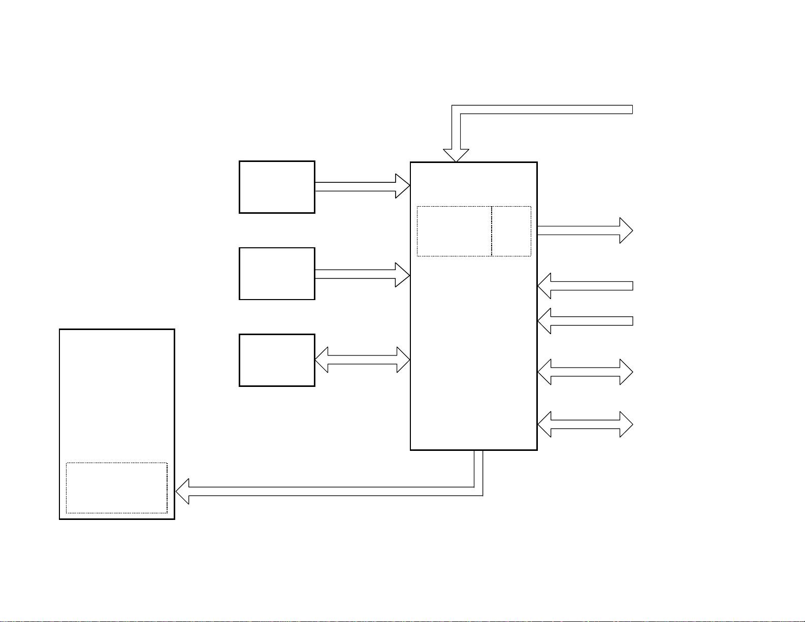
The block diagram of the C-003 frequency synthesizer (F/S) tuning system
and the BUS control circuits is shown in the diagram below. An outline of the
operation of each block is given below.
A. CPU
The CPU is the nucleus of the system, controlling each block according to the
signals input from the keyboard or remote control transmitter. The basic
function which the CPU controls are as follows:
1. Blanking and multi-color CRT signals for the on-screen displays
2. Time of Day clock and Sleep Timer function
3. Auto Program, Channel Memory function
4. Auto Shut-Off function (Turns TV OFF if no video signals are received
for 15 minutes)
5. TV/AV input switching function
6. Phase Locked Loop function (PLL) (programmable divider and phase
detector)
7. Power supply protection function
8. Digital control functions for picture and audio
9. Trilingual (English/Spanish/French) On-Screen menu system
10. AFT search function
11. Caption Data Slicer
12. V-Guide control function
13. Color Enhancer control function
14. On-screen Service Adjustment Menu system
15. Automatic RF AGC adjustment system
16. Automatic Bright Level adjustment system
17. Signal Processor BUS control function
18. MTS Processor control function
19. Front Surround control function
20. PIP control function
21. EEPROM control
B. Key Matrix
1. Produces DC voltages for the keyboard input.
C. BUS Control Output Circuit
1. Outputs the BUS data from the CPU to each control register within the
UHF/VHF tuner, the new Signal Processor, the new PIP Signal
Processor, and the new MTS Processor.
D. EEPROM (Nonvolatile Memory)
1. Stores channel memory, antenna mode, customer settings of digital
control, caption mode, and language mode.
2. Stores the BUS data used for factory/service adjustment.
E. RF AGC A/D Input Circuit
1. Detects and resistive divides the RF AGC voltage supplied from the
new Signal Processor to match with the A/D input of the CPU.
F. Beam Current Detector
1. Detects and converts the CRT beam current from the flyback
transformer to DC voltages for the A/D input of the CPU.
G. Remote Control Input
1. Amplifies and couples the remote control data to the CPU.
Page 5
– 3 –
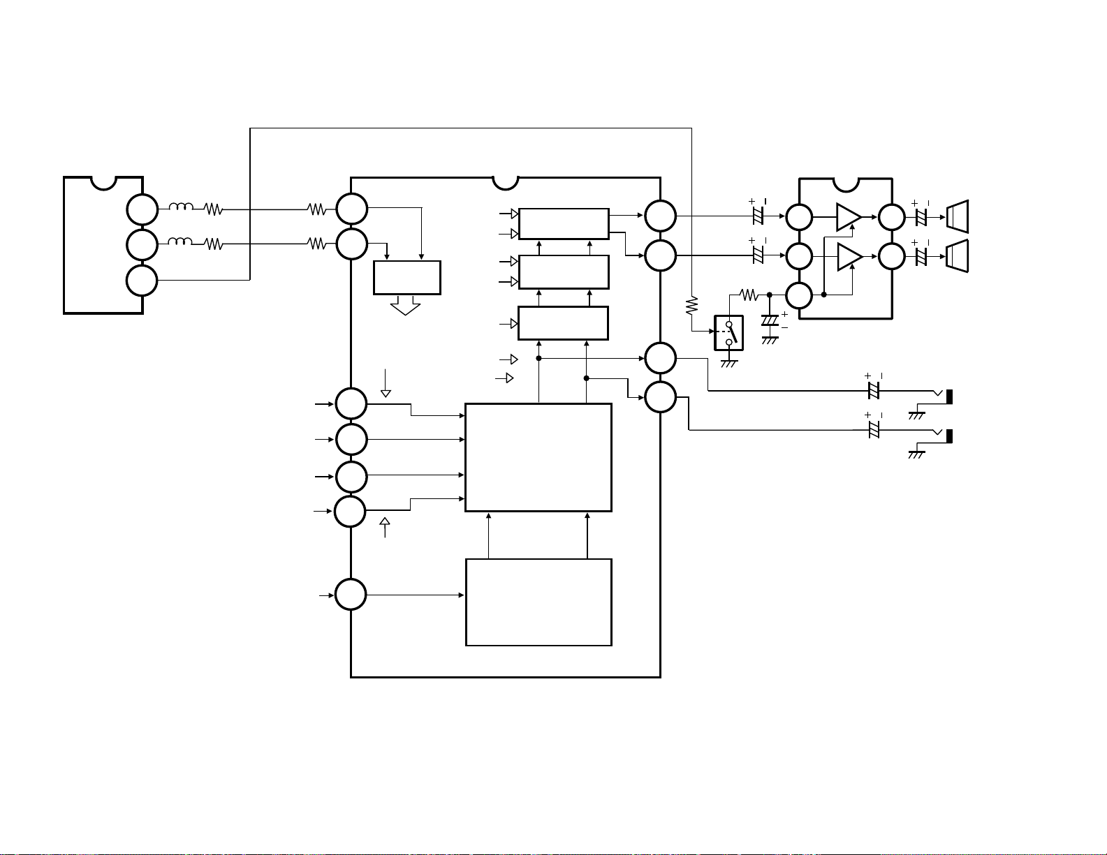
C-003 Tuning System Block Diagram
RC
PRE-AMP
COMPOSITE
VIDEO
TUNER
PLL
PRE-SCALER
BAND SW
KEY
BOARD
EEPROM
CAPTION
DATA SLICER
CPU
(C-003)
OSD
DISPLAY
RF AGC
A/D INPUT
BEAM CURRENT
DETECTOR
DIGICON
SOUND
AV
MTS
PIP
AFT
BUS CONTROLLED
SIGNAL PROCESSOR
Page 6
– 4 –
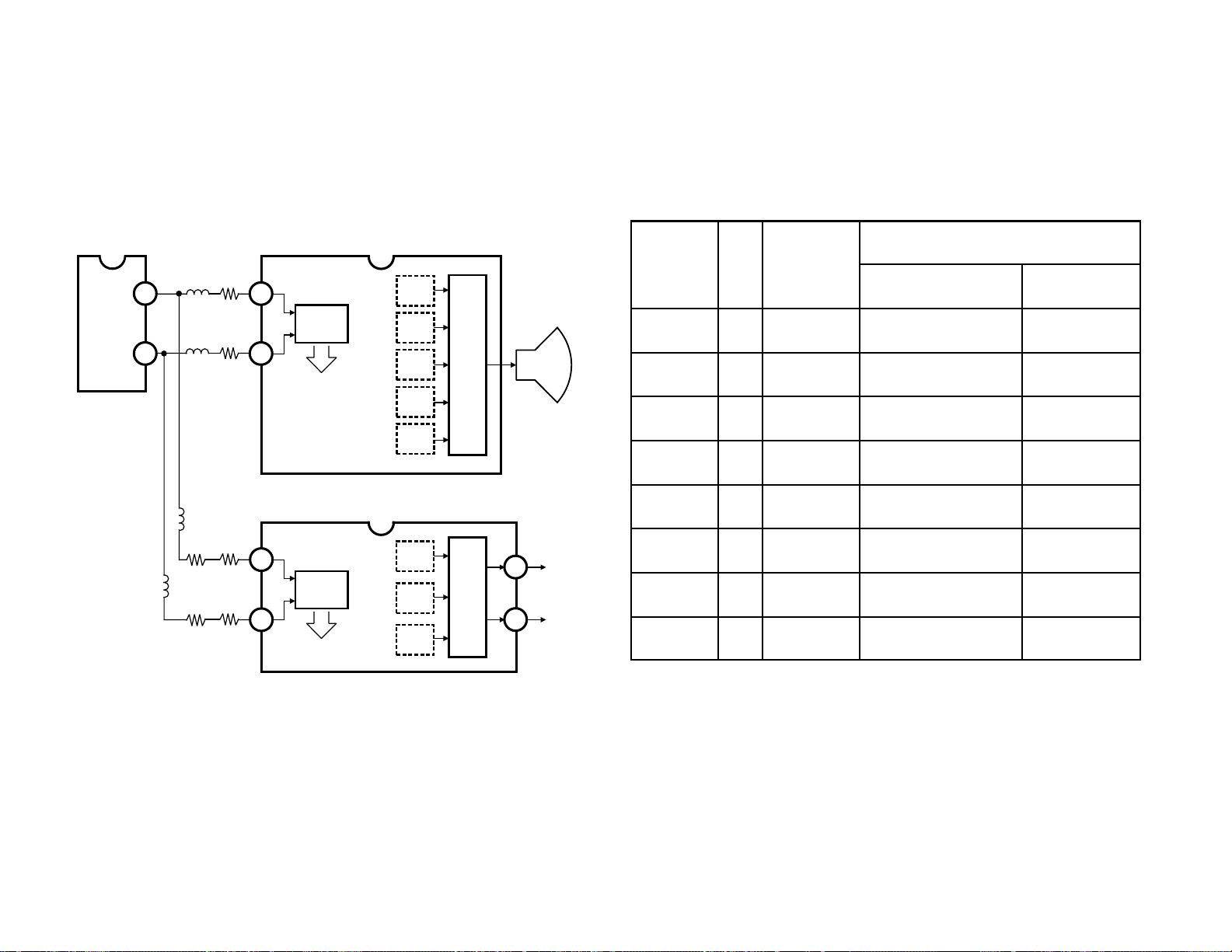
CPU PROGRAMMING
The On-screen Service Adjustment Menu system employed in the VB7C
chassis replaces the resistors used to change the voltage on the option pins
of the previous CPU. In order to program the CPU for the different options
available for the VB7C chassis, the On-screen Service Adjustment Menu is
used to change the option data in IC802, the EEPROM.
The Service Adjustment Menu display shown below and the following table
show the different options available and the necessary data. The option data
shown are for Mode AVM-2780G and include these options: with Clock, with
Surround, with Software for PIP Rating Information Processing, with Color
Enhancer, with Initial Channel, with PIP, with 2 AV Inputs, and with Bass &
Treble controls.
Memory Control Circuits
IC801
CPU
R808
ALWAYS
5V
L801
IC802
EEPROM
C801
IIC
SCL
IIC
SDA
33
31
R807
6
5
SCL
SDA
Page 7
– 5 –
PROGRAM CODES
The microprocessor used in the VB7C chassis is a multi-purpose type and is
used in several different models. To ensure proper operation and the correct
features for your particular model, the Program Codes must be correct.
Note: To enter the service adjustment menu, connect the AC power cord
while pressing the MENU key. The service adjustment can be made
with the remote control. To exit the service adjustment mode, press the
MENU key again. Refer to the specific Service Manual for your model
for complete adjustment procedure.
* . . . .When the Initial Channel option is used, the Initial Channel (the TV can
be set automatically to tune to a specific channel each time it is turned
on.) and XDS (Extended Data Service) features are available.
BIT FUNCTION
DATA
01
0 NOT USED
–– ––
1 NOT USED
–– ––
2 NOT USED
–– ––
00: NONE
3, 4 CLOCK 01: YES (AC 60 Hz)
10: YES (INT OSC)
11: INHIBITED (=NONE)
5 NOT USED
–– ––
6 SURROUND NONE YES
7 NOT USED –– ––
BIT FUNCTION
DATA
01
0 PIP RATING INFO.
–– ––
1 COLOR ENHANCER NONE YES
2 INITIAL CHANNEL NONE YES *
3 NOT USED –– ––
4 PIP NONE YES
5 AV1 / AV1, AV2 AV1 AV1, AV2
6 TONE / BASS, TREBLE BASS, TRE. TONE
7 NOT USED
–– ––
NO. DATA
XXX OPT XXX XXXXXXXX
DECIMAL DATA (ZERO SUPPRESSED)
NO. 29, 30
TITLE OPT, OP2
BINARY DATA (8 bit)
Option Data 1
Option Data 2
Page 8
– 6 –
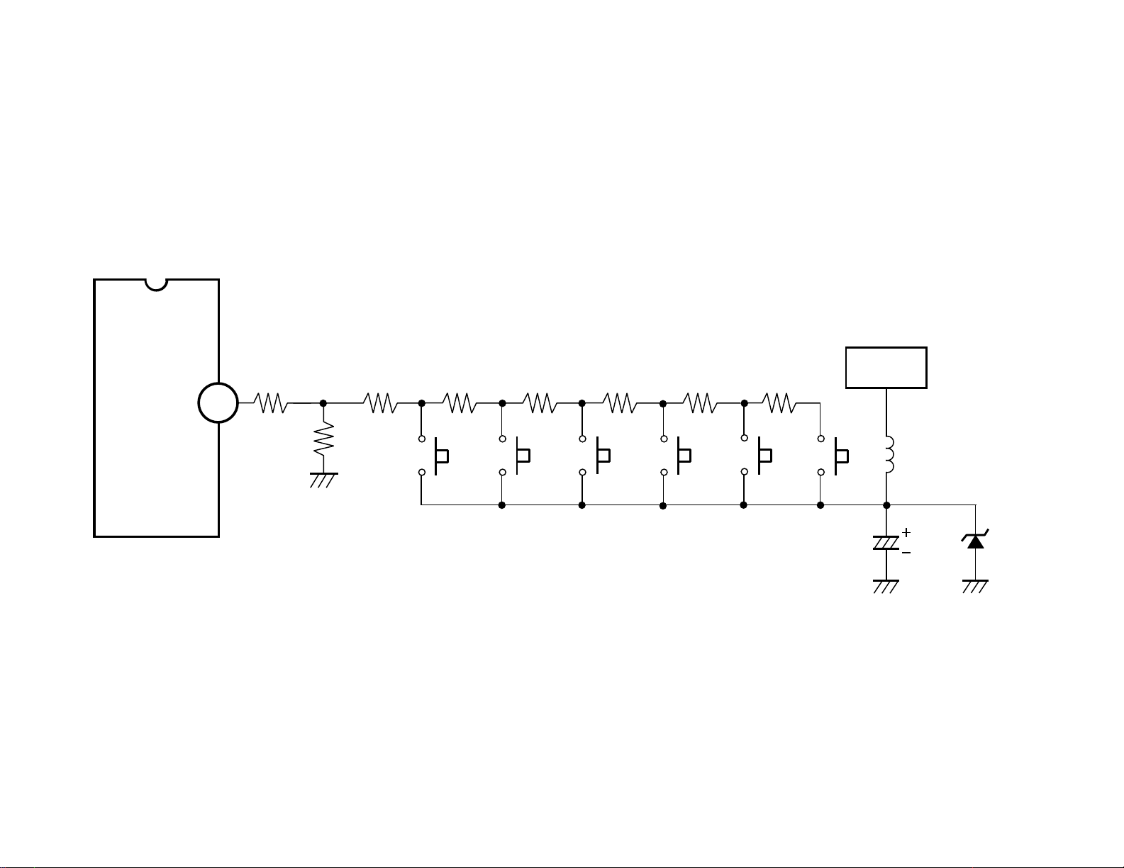
Key Scan
The Key Scan circuit uses an analog circuit to generate and send voltage to
the CPU when a key is pressed. The CPU uses this voltage to determine
which key was pressed. This resistive circuit eliminates the need for
encoder/decoder devices, simplifying design and adding to the reliability of
the receiver.
The CPU performs a key scan approximately every 20ms to check for a
pressed key. When the key data change is the same for two consecutive
reads, it is determined that a key has been pressed and the corresponding
command executed.
The table below shows the voltages input to CPU pin 9 when a given key is
pressed.
Key Input
The function of the keys on keyboard and those of the remote control
transmitter are the same.
The following keys, when activated, perform a series step action. The time of
each series step action is also shown below.
A . CH Up/Down 500 ms/step.
B . Vol Up/Down 140ms/step. It takes about 9 seconds to change from
minimum to maximum volume.
Preceding and succeeding mutes are performed when turning power Off/On,
changing channels, switching Antenna mode, searching channels, changing
MTS or TV/AV mode, exchanging programs between the main screen and
PIP window, or switching Surround sound mode.
Channel and Mode Change Mutes
Key Scan Voltages
KEY INPUT VOLTAGE FUNCTION
SW1901 4.26 ~ 5.00 POWER
SW1902 3.63 ~ 4.26 VOL +
SW1903 3.01 ~ 3.63 VOL SW1904 2.38 ~ 3.01
CH ▲
SW1905 1.60 ~ 2.38
CH ▼
SW1906 1.13 ~ 1.60 MENU
OFF 0.00 ~ 1.13
–––
KEY SCAN CIRCUIT
PRESSING KEY
MODE OUTPUT
MODE CHANGE
PRECEDING
MUTE
MUTE SIGNAL MUTE OFFMUTE ON
SUCCEEDING
MUTE
Page 9
– 7 –
IC801
Key Scan Circuit
CPU
ALWAYS
R1910
R1907R1906R1905R1904R1903R1902
5V
9
R1901
L1901
SW1901
(POWER)
SW1902
(VOL + )
SW1903
(VOL – )
SW1904
(CH ▲ )
SW1905
(CH ▼ )
SW1906
(MENU)
C1902
D1901
(7.5V)
Page 10
– 8 –
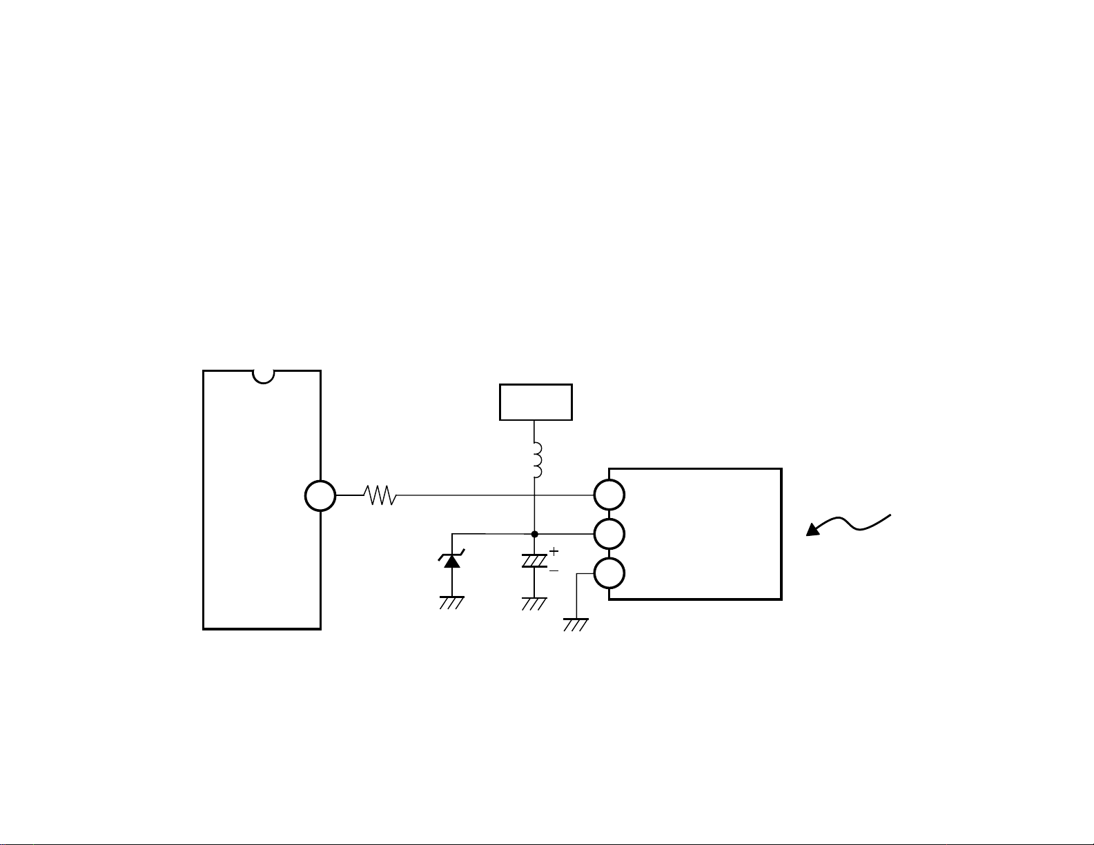
REMOTE CONTROL INPUT
The data received from the remote control is first amplified to 5 V digital
pulses by the pre-amplifier module A1901 and then input to the CPU on pin
10. See Remote Transfer Code figure below. The remote data is a transfer
code consisting of a leader code, an 8-bit custom code, and an 8-bit data
code. A signal transfer code is 32 bits which allows the custom and data
codes to be sent twice, once in the normal mode and then inverted. This
provides a type of redundancy check to prevent misoperation.
Custom and Data codes differentiate between the “1” and “9” values by the
pulse duration. See “1” and “0” Pulse Duration diagram below.
The custom code is a unique code assigned to each manufacturer.
Its purpose is to help prevent operation of the TV by remote controls for other
components such as VCRs, CD players etc. The code assigned to our
company is 38H. See Custom Code figure below. The data code is the
command, or channel number.
Remote Input Circuit
IC801
CPU
L1901
R1909
10
ALWAYS
5V
1
A1901
RC PRE-AMP
D1901
(7.5V)
2
C1902
3
Page 11
– 9 –
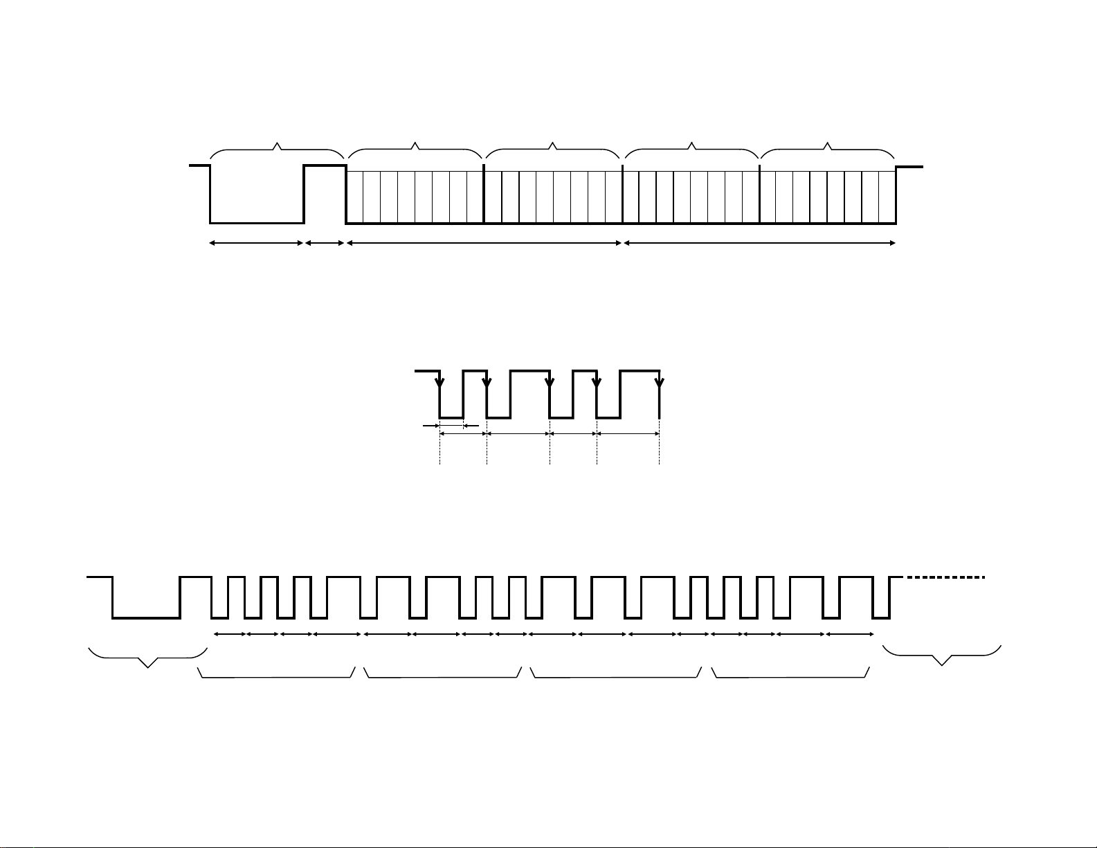
LEADER CODE CUSTOM CODE CUSTOM CODE DATA CODE DATA CODE
C0C1C2C3C4C5C6C7
Remote Transfer Code
0.56msms
1.125ms 2.25ms 1.125ms 2.25ms
" 0 " " 1 " " 0 " " 1 "
"1" and "0" Pulse Duration
D0D1D2D3D4D5D6D7
27ms9ms 4.5ms 27ms
0
000
LEADER CODE DATA CODE
111
00
111
00
1
1
Custom Code
Page 12
– 10 –
PLL DATA OUT CIRCUIT
The VB7C chassis uses a new BUS-Controlled UHF/VHF Tuner with a builtin Phase Locked Loop, Prescaler and Band Switch. Including these circuits
in the tuner reduced RF radiation and simplified shielding requirements and
printed wiring board layout. The primary difference between this chassis and
the previous chassis (C-983) is the exclusive PLL control lines (PLL Enable,
PLL Data, PLL Clock) are unified to the common BUS control lines (BUS SDA,
BUS SCL), and the BUS control program is incorporated in the CPU (C-003).
Channel selection requires only two inputs from the CPU. These are the Data
signal input from pin 32, and the Clock signal input from pin 34. The Data
signal controls the band switching, the channel selection and the AFT. The
channel selection and the AFT function are controlled by changing the divide
ratio for the PLL.
The tuning data format is composed of 5 byte data. See Tuning Data Format
figure below.
PLL Data Circuit
IC801
CPU
BUS
SDA
L881
32
R881
A101
TUNER
R856
DATA
BUS
SCL
34
L882
R882
R857
CLOCK
Page 13
– 11 –
BYTE (MSB) DATA BYTE (LSB) COMMAND
Address byte (ADB) 1 1 0 0 0 MA1 MA0 0 A
Divider byte 1 (DB1) 0 M9 M8 M7 M6 M5 M4 M3 A
Divider byte 2 (DB2) M2 M1 M0 S4 S3 S2 S1 S0 A
Control byte (CB) 1 CP T1 CD X 1 1 0 A
Band switch byte (BB) X X X X BU FMT BVH BVL A
PLL Data Format
A • • • • • • • • • • • • • • acknowledge
MA1 and MA2 • • • • • address selection bits
M8~M0, S4~S0 • • • • programmable divider bits
CP • • • • • • • • • • • • • charge pump current (tuning speed) switch control
T1 • • • • • • • • • • • • • test mode selection
CD • • • • • • • • • • • • • charge pump defeat switch control
X • • • • • • • • • • • • • • don’t care bit
BU • • • • • • • • • • • • • UHF band switch control
FMT • • • • • • • • • • • • FM trap (92.5MHz) switch control at channel 6
BVH • • • • • • • • • • • • VH band switch control
BVL • • • • • • • • • • • • VL band switch control
BAND BU FMT BVH BVL
VL (WITHOUT CH 06 ONLY) L L L H
VL (CH 06 ONLY) L H L H
VH L LHL
UHF H L L L
Band Switch Control Data
Page 14
– 12 –
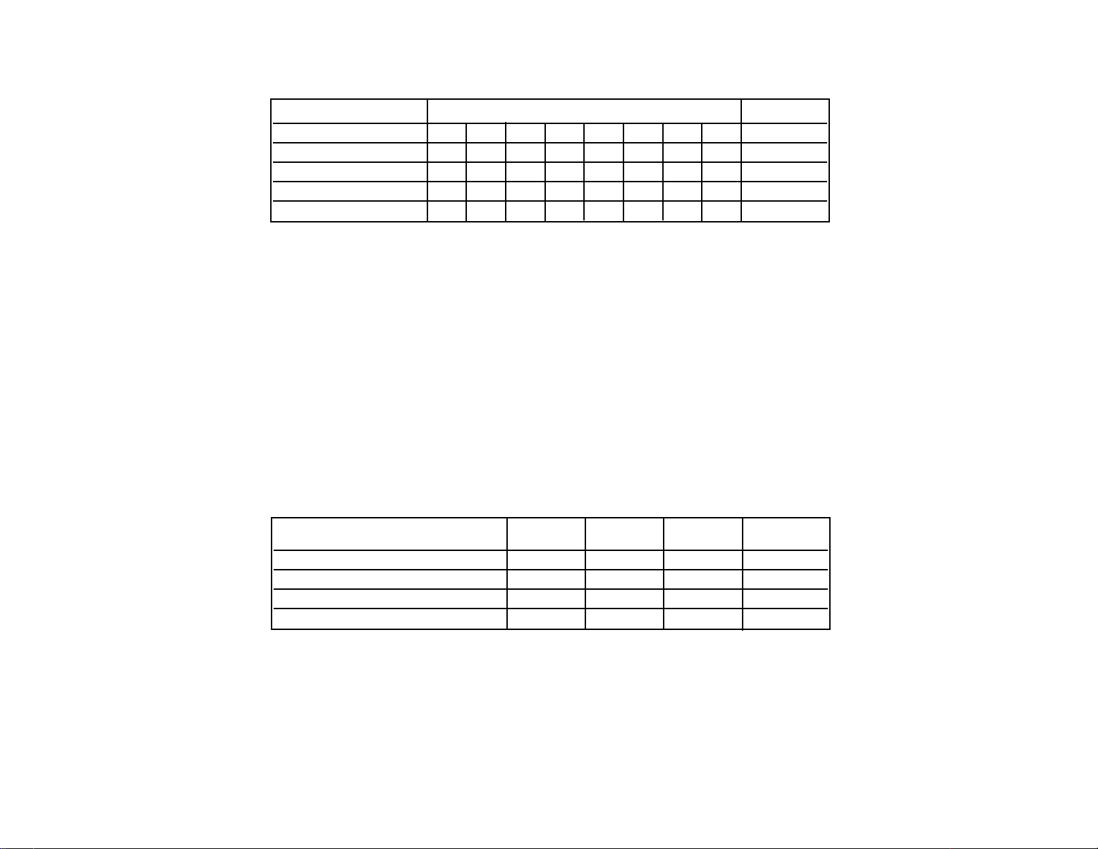
AFT CIRCUIT
The Automatic Fine Tuning (AFT) program incorporated in the CPU functions
to fine tune the tuner local oscillator to the center of the actual broadcast
frequency. This is necessary because the transmitted TV signal may not be
exactly on its assigned channel frequency. In addition, certain CATV
channels are purposely slightly offset to reduce interference from broadcast
frequencies. The operating range of the AFT is ± 2.25 MHz from FCC center.
Specifically, the AFT searches the frequency band ± 2.25 MHz from FCC
center in 62.5 KHz steps by changing the PLL division ratios while evaluating
the binary signals from IC101, the Signal Processor.
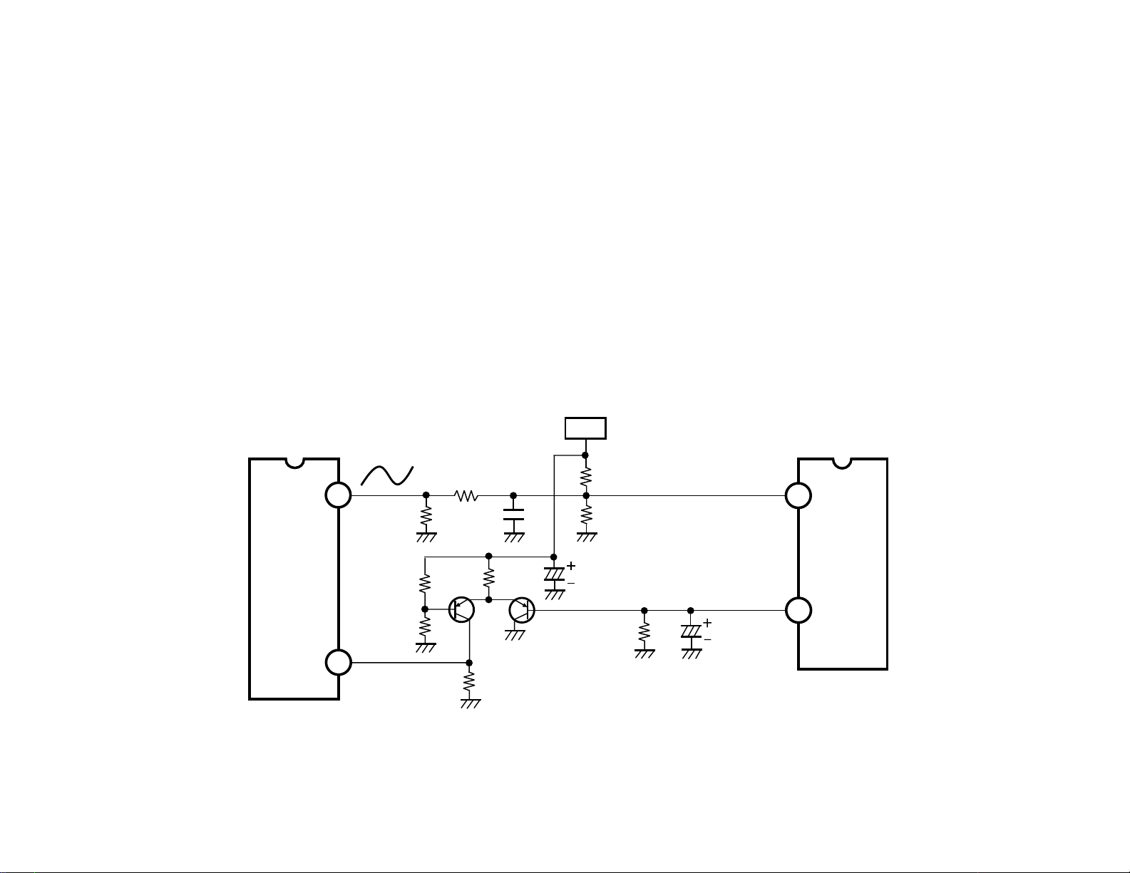
The station center is determined to have been found when the Time Base
signal at pin 26 is High and the AFT S-Curve signal at pin 29 is between 3.3
VDC and 1.67 VDC. However, the slope (right down) is also checked to
distinguish the station center from a pseudo-tuning point.
The Time Base signal is the AND signal of the horizontal sync signal from the
flyback transformer and the horizontal sync signal from the video (Y) signal.
The AFT S-Curve signal is an indication of the video IF carrier frequency
45.75 MHz.
The Time Base and AFT S-Curve signals are checked after each stepping
action. If station center cannot be confirmed after a complete search of the
upper and lower limits of the AFT range, the frequency is returned to FCC
center and the AFT action ceased.
The AFT only operates when first entering the channel. When entering the
channel C05 or C06, the operating range of the AFT is ± 2.25MHz from FCC
center +125 KHz (2 steps).
AFT Circuit
IC801
CPU
R167
AFT
S-CURVE
29
R168
C161
7.6 V
IC101
SIGNAL
PROCESSOR
R161
13
R162
TIME
BASE
26
R371
R377
Q372
R376
R372
Q371
C258
R373
18
C371
Page 15
– 13 –
CPU
RANGE OF 0 ~ 5 V
AFT
S-CURVE
TIME BASE
SIGNAL
3.3 V
1.67 V
TUNING
POINT
AFT S-Curve Signal
Time Base Signal
Station Center
Page 16
– 14 –
SIGNAL PROCESSOR BUS CONTROL CIRCUIT
The VB7C chassis is equipped with a new single-chip BUS-Controlled NTSC
Signal Processor IC to replace much of the mechanically adjusted
factory/service controls and all of the low pass filters in the PWM control lines
for the customer setting digital controls used in the conventional chassis.
The primary difference between this chassis and the conventional chassis is
the addition of the BUS Interface circuit and the movement of the control
registers into the Signal Processor IC, and the BUS control program
incorporated in the CPU (C-003).
The advantages of this chassis include reduced control lines and associated
circuitry, and improved productivity and increased accuracy of the factory
adjustments during production. This is due to the computerized and digitized
control circuit which allows remote operation.
Control of the Signal Processor IC is through CPU pins 32 and 34.
Pin 34 is the BUS SCL (Serial Data) signal. The BUS SDA is a bi-directional
signal and is used to transfer data into and out of the control registers within
IC101. Data is processed through an 8 bit read or write for each sub address
in an IC address “1011010” with in IC101.
See Bit Map below for IC Address,
Sub Address or Data for details.
IC801
CPU
BUS
SCL
BUS
SDA
34
32
L814
L813
SIGNAL PROCESSOR
R804
43
CLK
R803
44
DATA
IC101
BUS
Interface
STA
ICW SUB DA STO
STA = START Condition
ICW = IC Address* + Write
SUB = Sub. Address*
DA = Data*
STO = STOP Condition
Control
Registers
Signal Processor BUS Control Circuit
c
*
See Bit Map below for IC Address,
Sub Address or Data for details.
BUS Data Format In Write Mode
Page 17
– 15 –
Register Name Bits General Description
T Enable 1 Disable the Test SW & enable Video Mute SW
Video Mute 1 Disable video outputs
Sync Kill 1 Force free-run mode
ABL Defeat SW 1 Disable ABL function
AFC Gain 2 Select horizontal first loop gain
Horizontal Phase 5 Align sync to flyback phase
IF AGC SW 1 Disable IF and RF AGC
AFT Defeat 1 Disable AFT output
RF AGC Delay 6 Align RF AGC threshold
Video SW 1 Select Video Signal (INT/EXT)
PLL Tuning 7 Align IF VCO frequency
BNI Enable 1 Enable black noise inverter
Audio Mute 1 Disable audio outputs
APC Det Adjust 6 Align AFT crossover
V Count Down Mode 1 Selected vertical countdown mode
Vertical Test Enable 3 Selected vertical DAC test modes
Vertical DC 6 Align Vertical DC bias
Vertical Kill 1 Disable vertical output
Color Kill 1 Enable Color Killer
Vertical Size 6 Align vertical amplitude
Red Bias 8 Align Red OUT DC level
Green Bias 8 Align Green OUT DC level
Blue Bias 8 Align Blue OUT DC level
Blanking Defeat 1 Disable RGB output blanking
Red Drive 7 Align Red OUT AC level
Drive Test 1 Enable drive DAC test mode
Blue Drive 7 Align Blue OUT AC level
Color Difference Mode Enable 1 Enable Color difference mode
Brightness Control 7 Customer brightness control
Contrast Test 1 Enable Contrast DAC test mode
Contrast Control 7 Customer contrast control
Trap & Delay SW 1 Select luma filter mode
AutoFlesh Enable 1 Enable autoflesh function
Black Stretch Defeat 1 Disable black stretch
Sharpness Control 5 Customer sharpness control
Tint Test 1 Enable tint DAC test mode
Tint Control 7 Customer tint control
Color Test Enable 1 Enable color DAC test mode
Color Control 7 Customer color control
White Peak Limiter Enable 1 Disable White Peak Limiter
G Drive Reduction 4 Select Green OUT AC level
V Size Compensation 3 Selected Gain of V Size Compensation
Video Level 3 Align IF video level
FM Level 5 Align WBA output level
Audio SW 1 Select Audio Signal (INT/EXT)
Volume Control 7 Customer volume control
Control Register Descriptions
IC Address: BAh (10111010)
Sub Address (MSB) DATA (LSB)
D7
• • • • • •
D0 DA7 DA6 DA5 DA4 DA3 DA2 DA1 DA0
$00 ✻✻✻✻T_Enable ✻ Vid_Mute
SSnncc KKiilll
l
(tr0) 1 0 0
$01 ABL DEF AFC Gain H_Phase
(tr1) 1 1 1 0 1 1 1 1
$02 IF AGC SW
AAFFTTDDEEF
F RF_AGC_Delay (Note-1)
(tr2) 0 0 1 1 0 0 1 0
$03 VIDEO SW PLL TUNING
(tr3) 0 1 0 0 0 0 0 0
$04 N/I SW Audio_Mute APC DET ADJUST
(tr4) 1 0 0 1 1 1 1 1
$05 VCD MODE V_Test Ver_DC
(tr5) 0 0 1 0 0 0 0 0
$06
VVeerr KKiillllCCooll KKiilll
l Ver_size
(tr6) 0 0 1 0 0 0 0 0
$07 R_Bias (Note-2)
(tr7) 0 0 0 0 0 0 0 0
$08 G_Bias (Note-2)
(tr8) 0 0 0 0 0 0 0 0
$09 B_Bias (Note-2)
(tr9) 0 0 0 0 0 0 0 0
$0A BLK_DEF R-Drive
(tr10) 0 0 1 1 0 1 1 1
$0B Drv_Test B_Drive
(tr11) 0 0 1 1 0 1 1 1
$0C C_Diff
BBrriigghht
t
(tr12) 0 1 0 0 0 0 0 0
$0D Cot_Test
CCoonnttrraasst
t
(tr13) 0 1 1 1 1 1 1 1
$0E Trap&D_SW A Flesh Black ST
SShhaarrppnneesss
s
(tr14) 0 1 0 1 0 0 0 0
$0F Tin_Test
TTiinnt
t
(tr15) 0 1 0 0 0 0 0 0
$10 Col_Test
CCoolloor
r
(tr16) 0 1 0 0 0 0 0 0
$11 W Peak G Drive Reduction V-Comp.
(tr17) 1 1 0 0 0 0 0 0
$12 VIDEO LEVEL FM LEVEL
(tr18) 1 0 0 0 1 1 1 1
$13 AUDIO SW Volume
(tr19) 1 1 1 1 1 1 1 1
• The shaded data shows fixed data.
• The outlined data can be changed except during the Service Menu mode.
• The data except above can be set with the Service Menu.
• Note-1: shows the data that can be set with the Service Menu or the Automatic Adjustment Menu.
• Note-2: shows the data that can be set with the R/G/B Bias Adjustments in the Service Menu.
Bit Map
Page 18
– 16 –
MTS PROCESSOR BUS CONTROL CIRCUIT
The VB7C chassis is equipped with a new single-chip BUS-Controlled MTS
Processor IC to replace much of the mechanically adjusted factory/service
controls and all of the low pass filters in the PWM control lines for the
customer setting digital controls used in the conventional chassis. In addition,
the Bass, Treble and Volume control circuits have been also integrated into a
single-chip IC.
The primary difference between this chassis and the conventional chassis is
the addition of the BUS Interface circuit and movement of the control registers
into the MTS Processor IC, and the BUS control program incorporated in the
CPU (C-003).
The advantages of this chassis include reduced control lines and associated
circuitry, and improved productivity and increased accuracy of the factory
adjustments during production. This is due to the computerized and digitized
control circuit which allows remote operation.
Control of the MTS Processor IC is through CPU pins 32 and 34.
Pin 34 is the BUS SCL (Serial Clock) signal. The BUS SCL input is used to
clock all data into and out of IC101.
Pin 32 is the BUS SDA (Serial Data) signal. The BUS SDA is a bi-directional
signal and is used to transfer data into and out of the control registers within
IC3401. Data is processed through an 8-bit read or write for each sub
address in an IC address “10000100” (Read Address) or “10000101” (Write
Address) within IC3401.
See Bit Map below for IC Address,
Sub Address or Data for details.
IC801
CPU
IC3401
MTS PROCESSOR
STA
ICA SUB DA STO
BUS
SDA
L881
32
R3401
SDA
5
BUS
R881
Interface
BUS
SCL
34
L882
R882
R3402
6
SCL
Control
Registers
MTS Processor BUS Control Circuit
STA = START Condition
ICA = IC Address* + Read or Write
SUB = Sub. Address* (needed only in Write mode)
DA = Data*
STO = STOP Condition
c
*
See Bit Map below for IC Address,
Sub Address or Data for details.
BUS Data Format in Write Mode
Page 19
– 17 –
IC Write Address: 84h (10000100)
Sub Address (MSB) DATA (LSB)
D7
• • • • • •
D0 DA7 DA6 DA5 DA4 DA3 DA2 DA1 DA0
00h ✻✻TEST-DA TEST 1 ATT (Note-1)
00
01h ✻✻ SPECTRAL (Note-2)
02h ✻✻ WIDEBAND (Note-2)
03h ✻ M2 EXT1 EXT2 NRSW FOMO SAPC M1
(Note-5) (Note-3) (Note-3) (Note-4) (Note-4) 0 (Note-5)
04h ✻ PSW ✻ SURR ATT SW ✻ FEXT1 FEXT2
0 (Note-6) 0 0 0
05h ✻✻ BASS (Note-7)
06h ✻✻ TREBLE (Note-7)
07h ✻✻ VOL-L (Note-8)
08h ✻✻ VOL-R (Note-8)
• Note-1: ATT for the Input Level Adjustment.
• Note-2: SPECTRAL for the High Separation and WIDEBAND for Low Separation
Adjustments.
• Note-3: EXT1 and EXT2 for the AV Selection.
• Note-4: NRSW for Stereo/SAP Selection and FOMO for Forced Mono Selection.
Mode EXT1 EXT2
TV 0 0
AV1 1 0
AV2 1 1
Mode selected Receiving Signal NRSW FOMO Output Signal
MONO Mono 0 ✻ MONO
Stereo 0 1 MONO
SAP + Mono 0 1 MONO
SAP + Stereo 0 1 MONO
STEREO Mono 0 1 MONO
Stereo 0 0 STEREO
SAP + Mono 0 1 MONO
SAP + Stereo 0 0 STEREO
SAP Mono 0 1 MONO
Stereo 0 0 STEREO
SAP + Mono 1 0 SAP
SAP + Stereo 1 0 SAP
• Note-5: M1 for TVOUT Mute and M2 for LSOUT Mute functions. LSOUT Mute is
accomplished by M2 and Volume Mute.
Mode Data
MUTE ON 0
MUTE OFF 1
• Note-6: SURR for Surround On/Off Selection.
Mode Data
SURROUND OFF 0
SURROUND ON 1
• Note-7: BASS for Bass Control and TREBLE for Treble Control.
Control Level Data
MAXIMUM 3Fh (111111b )
CENTER 1Fh (011111b)
MINIMUM 00h (000000b)
• Note-8: VOL-L for L-Channel Volume Control and VOL-R for R-Channel Volume
Control.
IC Read Address: 85h (10000101)
Bit 7 Bit 6 Bit 5 Bit 4 Bit 3 Bit 2 Bit 1 Bit 0
POWER STEREO SAP NOISE –– –– –– ––
✻: Don’t care bit.
POWER=1 : Reset
STEREO=1 : Stereo is present.
STEREO=0 : Stereo is absent.
SAP=1, NOISE=0 : SAP is present.
SAP=1, NOISE=1 : SAP is absent.
SAP=0 : SAP is absent.
Page 20
– 18 –
SOUND CONTROL CIRCUIT
The sound level is controlled by the BUS control signal form the CPU, the
BUS SDA (Serial Data) signal from pin 32, and the BUS SCL (Serial Clock)
signal from pin 34. The BUS control signals from the CPU are coupled to the
BUS Interface circuit within IC3401, the MTS Processor. The BUS Interface
circuit transfers a 6-bit volume data into both of the Volume Control Registers
VOL-L and VOL-R. A 6-bit volume control data from each of the Volume
Control Registers is converted to a 0-63 steps analog signal (DC voltages) in
the Volume D/A converter for input to the Volume Control Circuit. Now the
audio signal is output from pins 3 and 4 of IC3401.
The volume control data “000000” and the audio mute control data “0” are
input to the Volume Control Registers VOL-L and VOL-R, and the Audio Mute
Control Register M2 (Sub Address 03h, Bit 6), respectively to set the output
sound level to step 0/63 during Mute ON. (See page 30 for the Audio Mute
Control Register M2.)
In addition, the CPU outputs the Mute (High) signal from pin 38 to prevent
buzz or static in the speakers when turning On/Off or during Standby mode.
The Mute (High) is coupled to the base of Q001, switching Q001 On,
grounding pin 5 of the Audio Amplifier IC001.
BUS Data Format in Write Mode - Volume Level at 16/63 step
STA ICW SUB DA STO
D6
D5
D4
D7 D0D1D2D3
D0D1D2D3
D7
D6
D5
00000011
STA: START Condition
ICW: IC Address + Write
SUB: Sub. Address
DA : Data
STO: STOP Condition
D4
DA7
1000001
✻✻010000
1
DA6
DA5
DA4
DA1
DA2DA3
(LSB)(LSB) (LSB) (MSB)(MSB)(MSB)
DA0
IC WRITE ADDRESS
D6
D5
D4
D7
D6
D7 D0D1D2D3
SUB. ADDRESS
D5
D4
00000011 00100000
IC WRITE ADDRESS
SUB. ADDRESS
Don't care bits
DA7D0D1D2D3
DA6
DA5
DA4
VOL-L
(LSB)(LSB) (LSB) (MSB)(MSB)(MSB)
DA0DA1DA2DA3
✻✻010000
Don't care bits
VOL-R
Page 21
– 19 –
Sound Control Circuit
IC801
CPU
BUS
SDA
BUS
SCL
MUTE
32
34
38
L881
L882
R881
R882
R3401
R3402
AV1-R
AV1-L
AV2-R
33
34
36
5
6
BUS
Interface
to BUS Line
FEXT1
IC3401
MTS PROCESSOR
VOL-R
VOL-L
TREBLE
BASS
SURR
M2
EXT1/EXT2/M1
VOLUME
CONTROL
BASS/TREBLE
CONTROL
SURROUND
BLOCK
AUDIO SW
3
4
38
39
IC001
AUDIO AMP.
C002
R
L
8
10
C001
C007
R011
R012
R
L
Q001
MOMENTARY
MUTE
5
C3437
C3435
C010
SP901
3
1
C011
R
SPEAKER (R)
SP902
L
SPEAKER (L)
K1011
FIXED
AUDIO OUT (R)
K1021
FIXED
AUDIO OUT (L)
AV2-L
SIF In
37
13
FEXT2
MTS DECODER
BLOCK
Page 22

– 20 –
DIGITAL CONTROL CIRCUITS
Digital electronic controls replace the mechanical customer controls. This
provides a more precise setting of the controls as well as allowing the
convenience of remote operation. The BUS data output from the CPU for
each Control Register are essentially the same as those previously described
for the Sound Control Circuit.
The BUS Interface circuit (see diagram below) is necessary to transfer each
control data in the BUS data from the CPU into a corresponding Control
Register in the Signal Processor IC101, and the MTS Processor IC3401.
After accessing the on-screen main menu system with the MENU key and
selecting the Picture/Sound Manual adjustment menu with the CH ▲ / ▼ and
VOL – / + keys, digital control is carried out by pressing the MENU key for
seven separate controls. the CH ▲ / ▼ key is used to select the control to
be changed. Each time a CH ▲ / ▼ key is pressed, the mode will advance
to the next control. The sequence is: Color, Tint, Contrast, Brightness,
Sharpness, Bass and Treble. the active control will be displayed on the
screen and then can be adjusted with the VOL – / + keys.
It takes 140 ms per step to change the control level with the VOL – / + keys.
There are 64 step control level changes in each control mode with the output
characteristics of each control mode independent of the others. When a VOL
– / + key is pressed it takes approximately 5 seconds to change from center
to minimum or center to maximum. The BUS data changes for the controls
are the same as those shown for the volume control.
When the FACTORY PRESET mode is selected with the RESET key, the
Picture/Sound controls will return to the factory settings. During FACTORY
PRESET mode the settings are as follows: COLOR 32/64*
1
, TINT 32/64*1,
CONTRAST 64/64*
2
, BRIGHTNESS 32/64*3, SHARPNESS 32/64*4, BASS
32/64, TREBLE 32/64. Furthermore, the FACTORY PRESET mode clears all
the other customized settings.
When the FACTORY PRESET mode is selected, the customized settings of
the digital controls will be reset. If desired, customized settings can be made
again using the on-screen menu.
*
1
A 7-bit control data up to 127 steps are output for each control register.
One and one half of the customer control steps (1.5x64 =96 steps) are
assigned for customer setting and the remainder (31 steps) are
provided for service adjustment.
*
2
A 7-bit control data up to 127 steps are output for this control register.
One and one half of the customer control steps (1.5x64 =96 steps) are
assigned for customer setting and the remainder (31 steps) are always
output.
*
3
A 7-bit control data up to 127 steps are output for this control register.
64 steps are assigned for customer setting and the remainder (63
steps) are provided for service adjustment.
*
4
A 5-bit control data up to 31 steps are output for this control register.
One fourth of the customer control steps (1/4x64=16 steps) are
assigned for customer setting and the remainder (15 steps) are
provided for service adjustment.
Page 23
– 21 –
Output Range of BUS Data
IC801
FUNCTION BTS
OUTPUT
RANGE OF
BUS DATA
RANGE OF STEPS
CUSTOMER
CONTROL
SERVICE
ADJUSTMENT
Color 7 0 ~ 127
(0~64)/127x1.5
=0/127~96/127
(0~31)/127
=0/127~31/127
Tint 7 0 ~ 127
(0~64)/127x1.5
=0/127~96/127
(0~31)/127
=0/127~31/127
Contrast 7 31 ~ 127
(0~64)/127x1.5+31/127
=31/127~127/127
(0)/127
=0/127
Brightness 7 0 ~ 127
(0~64)/127
=0/127~64/127
(0~63)/127
=0/127~63/127
Sharpness 5 0 ~ 31
(0~64)/31x1/4
=0/31~16/31
(0~15)/31
=0/31~15/31
Volume 6 0 ~ 63 0/63~63/63 ––
Bass 6 10 ~ 54 10/63~54/63 ––
Treble 6 10 ~ 54 10/63~54/63
––
CPU
BUS
SDA
BUS
SCL
32
34
L813
L814
R803
R804
44
43
SIGNAL PROCESSOR
IC101
Color
BUS
Interface
to BUS Line
Tint
Contrast
Brightness
Sharpness
Write
7 bit
Write
7 bit
Write
7 bit
Write
7 bit
Write
5 bit
CRT
Video/Chroma
Processing Circuit
R881
L882
R882
L881
R3401
5
R3402
6
Digital Controls
IC3401
MTS PROCESSOR
Volume
-L/R
BUS
Interface
to BUS Line
Treble
Bass
Write
6/6 bit
Write
6 bit
Write
6 bit
3
MTS Signal
4
Processing Circuit
R-OUT
L-OUT
Page 24

– 22 –
POWER ON/OFF and PROTECTION CIRCUITS
Power On/Off
The CPU performs the On/Off function through pin 27. In the Power On mode
pin 27 changes from Low to High, forward biasing Q681. When Q681
switches On, the base of Q627 will become Low, forward biasing Q627.
When Q627 (+12V Sw.) switches On, forward bias will be applied to Q486
(+9V Reg.). When Q627 switches On, current will flow through relay RL601,
closing the contacts and applying AC power to the degaussing circuit.
In the Power Off mode, pin 27 of the CPU will become Low. Q681 will now
be switched Off, switching Off Q627. Then Q486 (+9V Reg.) will switch Off.
With Q627 Off, current will cease to flow through RL601, opening the
contacts.
Power Supply Protection
The C-003 CPU provides a power source protection function to automatically
switch Off the power if an abnormal condition occurs in the chassis power
supplies to help prevent secondary damage.
Detection of an abnormal condition is accomplished by monitoring the +4.8V
(IC301 VDD), +7.6V and the +9V DC supplies at pin 3 of the CPU.
Pin 3 is normally High, approximately 5V (Vcc). If, while the power is On, pin
3 becomes Low (0.4 VCC or less) for a continuous period of approximately 1.5
seconds, pin 27 (power) of the CPU will be switched Low, shutting Off the
power.
If, while the power is Off, the power is switched On and pin 3 remains Low for
a period of approximately 3.0 seconds, pin 27 will be switched Low, shutting
Off the power.
In circuit operation, if all +4.8V, +7.6V and +9V supplies are their normal
potential, the diodes D312, D801, and D489 will be reversed biased. With all
diodes Off, a High of 5V will be input to pin 3 of the CPU. Should either +4.8V,
+7.6V, or +9V supply become 2V or less, one of the diodes will switch On,
forcing a Low at pin 3 of the CPU. The input to pin 3 is evaluated every 20
ms.
Note: The C-003 CPU provides a Power Surge Protection feature. If power
failures occur three times within 15 minutes, the CPU will automatically
stop functioning to help prevent secondary damage. (TV will not turn
On by pressing the POWER key.) To reset the operating programs
within the CPU, disconnect the AC power cord for at least 10 seconds.
Auto Shut Off Function
The Auto Shut Off feature operates to switch the TV Off if no video signal is
received for a certain period of time. The Time Base signal is used within the
CPU to determine the presence of an active channel. If pin 26 of the CPU
goes Low for a continuous period of approximately 15 minutes, the CPU
program will determine that no active channel is present and activate the Auto
Shut Off feature. The Auto Shut Off has priority over the Sleep Timer function,
however, it is inactive when the TV is in the AV (Video) mode.
Anode Current Leak Protection
The VB7C chassis provides an anode current leak protection circuit to
automatically switch Off the power to help prevent the risk of fire if an
abnormal condition such as high voltage arcing occurs on the picture tube
anode or in the high voltage circuits due to accumulated dust or liquid spilled
into the TV cabinet.
Detection of an abnormal condition is accomplished by monitoring the Heater
voltage supply at pin 3 of the CPU. Since the high voltage arcing on the
picture tube anode or in the high voltage circuits causes excessive current
flows and lower voltage supplies from the secondary windings of the Flyback
Transformer (T402), the excessive current flows are effectively monitored.
In circuit operation, the normal potential Heater voltage, approximately
22VDC higher than the zener voltage (15V) of D428, is applied to the cathode
of D428, diode D429 will be reversed biased.
With D429 Off, a High of 5V will be input to pin 3 of the CPU. Should the
cathode voltage of D428 become 15.2V or less, D429 will, switch On, forcing
a Low at pin 3 of the CPU.
Page 25

– 23 –
Power and Protection Circuits
TIME BASE
26
IC801
CPU
POWER
ON/OFF
TIME
BASE
POWER
FAIL
27
3
+12V
B4
ALWAYS
+5V
R852
C629
R835
C683R683
TJ2
R628
Q681
IC681
+5V REG
D801
D312
Q627
R627
D680
R629
R691
D629
(20V)
+7.6V
+4.8V
D311
(5V)
C626
R311
L623
D683
TJ7
D493
(7.5V)
D624
POSISTOR
R498C497C258
R310
R489
RL601
PS601
T601 (POWER)
AC IN
L901
DEGAUSSING
COIL
TJ5
D489
(7V)
R428
+9V
D428
(15V)
C484D429
D482
D486
(10V)
R482
Q486
R486
R487
T402 (F.B.T)
CRT HEATER
R497
Page 26

– 24 –
TV/AV SWITCHING CIRCUITS
The VB7C chassis (AVM-2780G) provides for the input of Auxiliary Video and
Audio signals.
When the AV1 or AV2 mode is selected from the remote control, pin 8 of the
CPU will go High. The High from pin 8 is coupled to the base of Q216. The
High coupled to the base of Q216 will switch Q216 On and ground the base
of Q343, the Band Pass Switch. The Low at the base of Q343 will switch
Q343 Off, cutting off L341 and C343 from the Band Pass Filter. This will
flatten the response curve of the Band Pass Filter to compensate for the
differences in the frequency characteristics of the AV video signal and the TV
video signal. This compensation will help to maintain a constant chroma
signal (3.58 MHz) gain.
The selection of the TV Audio, AV1 Audio or AV2 Audio signal is controlled by
the MTS Processor IC3401 through the CPU IC801. All of the TV, AV1 and
AV2 audio inputs are applied to an audio switch within IC3401 which is
controlled by the BUS interface.
CPU TV/AV Switching Signal
The selection of the AV1 S-Video, AV1 Composite Video, or AV2 Video signal
is controlled by the CPU and the mechanical switch of AV1 S-Video input jack
K1051.
When the AV1 is selected, pin 5 of the CPU will be Low. When the AV2 is
selected, pin 5 of the CPU will go High.
When the AV1 S-Video is connected during AV1 mode, pin 10 of IC1001 and
pin 12 of the CPU will be forced Low. With the Low at pin 12, the CPU will
regard the S-Video as connected and output the High signal from pin 4.
The selection of the TV Video or AV Video signal in the Signal Processor
IC101 is controlled by the CPU IC801. Both of the TV and AV video signals
are applied to an input switch within IC101 which is controlled by the BUS
interface. Either of the video signals is applied to the Comb Filter IC301 and
coupled to the Main S1/V1/V2 Switch IC1081.
Note: • Using the AV1 S-Video Input jack overrides the AV1 Composite
Video Input jack during the AV1 mode.
TV/AV Mode Switching Signal
AV1
MODE TV S-VIDEO COMPOSITE AV2
VIDEO
CPU (4) L H L L
CPU (5) –– L L H
CPU (8) L H H H
CPU (12) H L H H
CPU (6) –– L L H
CPU (7) L H H H
AV1
MODE TV S-VIDEO COMPOSITE AV2
VIDEO
IC1001 (9) –– L L H
IC1001 (10) H L H H
IC1001 (11) H H H H
IC1002 (9) –– L L H
IC1002 (10) –– L L H
IC1002 (11) L H H H
IC1081 (9) L H L L
IC1081 (10) L H L L
IC1081 (11) –– L L H
Page 27

– 25 –
TV
TV/AV Switching Circuit
ANT
K1051
S1 IN
K1002
V2 IN
K1001
V1 IN
C
A101
TUNER
Q162
1ST
VIDEO
SIGNAL PROCESSOR
10
11
45
47
1
EXT V IN
INT V FOR PIP
Y
IC101
BUS
Interface
VIDEO
DET.
44
43
38
40
42
Q202
BUFFER
Y
C
Q8065
BUFFER
Q306
BUFFER
INPUT
FILTER
Q307
BUFFER
+9V
IC1001
S1/V1/V2
SWITCH
V1
IC801
CPU
BUS SDA
32
BUS SCL
34
MUTE
38
TV/AV
8
16 15 14 13 12 11 10 9
HLH L
1 2 3 4 5 6 7 8
S1-SW
MAIN AV1/AV2
PIP TV/AV
PIP AV1/AV2
MAIN S SELECT
Y1
12
5
7
6
4
R1027
V2
HL
C1C1
R1007
Q8073
BUFF.
INPUT
FILTER
Q8097
BUFFER
Q8093
BUFFER
Q8090
BUFFER
Q8076
BUFFER
Q1071
BUFFER
PIP SIGNAL PROCESSOR
SCL
25
SDA
ACK
PIP
CVBS IN
MAIN Y
MAIN C
Y OUT
C OUT
Interface
24
23
13
49
51
47
SWITCH
45
BUS
YC SEP
PIP
IC8001
PROCESSOR
PIP
FIXED AUDIO OUT (R)
FIXED AUDIO OUT (L)
K1011
K1021
SP901
SPEAKER (R)
SP902
SPEAKER (L)
(R)
(L)
IC001
AUDIO AMP.
3
1
IC3401
MTS PROCESSOR
R
38
L
39
R
3
L
4
8
10
5
6
13
34
37
33
36
SDA
SCL
TV COMP.
AUDIO (L)
AV1 AUDIO(L)
AV2 AUDIO(L)
AV1 AUDIO(R)
AV2 AUDIO(R)
5
Q001
MOMENTARY
MUTE ON/OFF
+9V
IC1002
PIP
COMPO.
VIDEO
SWITCH
+9V
IC1081
MAIN
S1/V1/V2
SWITCH
EXT.V
R1041
16 15 14 13 12 11 10 9
HLH L
1 2 3 4 5 6 7 8
C
16 15 14 13 12 11 10 9
HLH L
1 2 3 4 5 6 7 8
C1
HL
R1082
HL
Y
R1042
R1081
Q1093,
C
Q1094,
Q1096
Y
Y(COMB)
C(COMB)
YC MIX
Q332
BUFFER
Q342
BUFFER
Q343
BAND
PASS
SW
BAND PASS
FILTER
IC301
15
COMB
FILTER
13
Q341
BUFFER
LPF
Q216
INVERT.
4
Page 28

– 26 –
REFERENCE OSCILLATOR
REFERENCE OSCILLATOR
The CPU requires a stable oscillator to serve as the clock signal. This clock
signal will be used to control the timing of all CPU functions and control
pulses. X801 connected between pins 19 and 20 of the CPU, provides a
stable, crystal controlled oscillator frequency of 8 MHz that is used for the
clock signal.
TIME DISPLAY FEATURE
The C-003 CPU provides a time display feature. The time of day clock is
timed by counting the reference oscillator frequency of 8 MHz served to the
CPU. The oscillator frequency is maintained accurate within ± 0.003 percent,
which provides a convenient and accurate timing signal for the clock. The
Clock and the Sleep Timer cannot be set if this timing signal is missing,
because of no signal to control the timing of all CPU functions and control
pulses.
8 MHz Reference Oscillator
C809
X801
C808
IC801
CPU
19
20
Page 29

– 27 –
CRT DISPLAY CIRCUIT
The CPU generates and controls all characters and data for the on-screen
displays. Excluding Captions, the VB7C chassis is designed for a green, red,
white, yellow and cyan screen display. In order to provide correct positioning,
vertical and horizontal sync signals are input to IC801 (CPU) on pins 1 (Hsync) and 2 (V-sync). The horizontal and vertical sync pulses are limited and
wave shaped by Q882 and Q881 respectively.
Operation
Beginning with the input of the vertical sync signal, horizontal sync pulses are
counted. After counting a certain number of horizontal sync pulses, the CPU
will begin counting 8 MHz clock pulses developed at pins 19 and 20. At the
desired number of clock pulses, the letter signals are output on pins 40-42,
and the blanking signals are output on pin 39. The letter and the blanking
signals are output as active Highs. The exact count of horizontal sync pulses
and 8 MHz clock pulses is controlled by the CPU program and will change
with the display pattern.
All display signals from the CPU are input to IC101, the Signal Processor, on
pins 33-36 where they are added to the video signal. Since the C-003 CPU
includes the Caption Data Slicer and Caption OSD, the screen displays and
caption displays cannot be shown simultaneously.
Screen Display Control Circuit
IC801
CPU
R-OUT
G-OUT
B-OUT
BLK-OUT
42
41
40
39
IC101
SIGNAL PROCESSOR
R849
R848
R847
R846
C843
33
R844
C842
34
R843
C841
35
R842
36
(8 MHz)
C809
C808
X801
ALWAYS
5V
R821
Q882
Q881
19
20
H-SYNC
X-IN
X-OUT
V-SYNC
1
R826
2
R827
R822
C832 R828
C831
R823
T402
5
IC501
7
Page 30

– 28 –
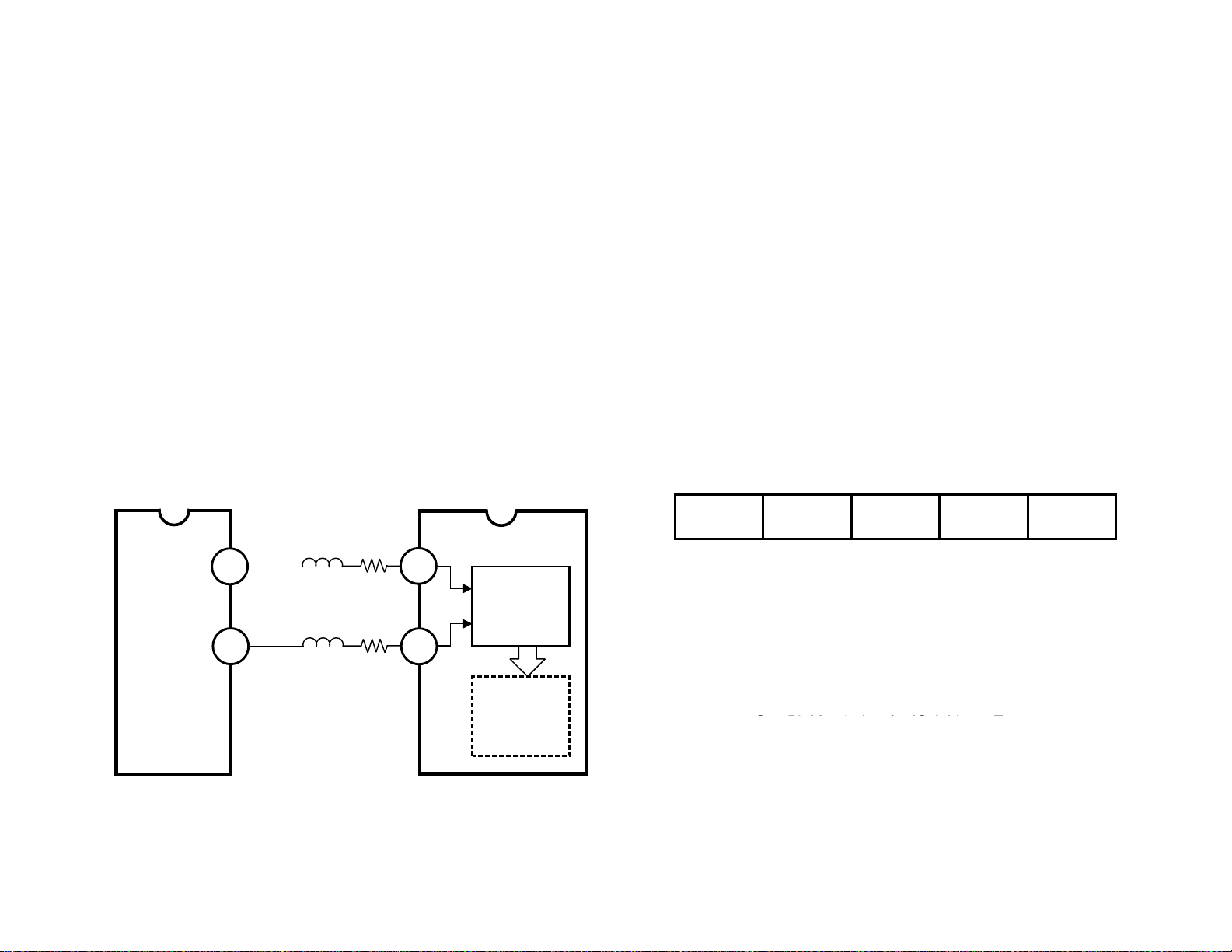
MEMORY CONTROL CIRCUIT
The VB7C chassis is equipped with a nonvolatile memory IC to store certain
information that should remain intact through a power failure. IC802 is the 2K
bit serial EEPROM used to store this information. An EEPROM or E2PROM
is an Electrical Erasable Programmable Read Only Memory integrated circuit.
IC802 will store Channel Memory, including active and inactive channels for
total of 125 channels, the Air/Cable mode, the customer settings of Digital
Control, Caption mode, Language mode, TV/AV mode, Surround On/Off
mode, Color Enhancer mode, the Line-SW On/Off mode, and the BUS data
used for factory/service adjustments. (The Line-SW On/Off mode is a special
mode used only for production.)
Control of the memory IC is through CPU pins 31 and 33.
Pin 33 is the IIC SCL (Serial Clock) signal. The IIC SCL input is used to clock
all data into and out of IC802.
Pin 31 is the IIC SDA (Serial Data) signal. The IIC SDA is a bidirectional
signal and is used to transfer data into and out of memory. Data is processed
through an 8 bit read or write for each address and there are 256 addresses.
Therefore, IC802 has a capacity of 256 x 8 or 2K bits of data.
Memory Control Circuit
IC801
CPU
R808
ALWAYS
5V
L801
IC802
EEPROM
C801
IIC
SCL
IIC
SDA
33
31
R807
6
5
SCL
SDA
Page 31

– 29 –
CPU
CPU
CPU
CPU
S1 100 00000
S
T
DEVICE CODE
A
R
T
CONTROL BYTE
READ/WRITE
NOTE : ACK=ACKNOWLEDGE BIT
S1 100 00000
S
T
DEVICE CODE
A
R
T
CONTROL BYTE
A
C
K
READ/WRITE
A
C
K
WORD
ADDRESS(n)
WORD
ADDRESS(n)
A
C
K
DATA n DATA n+1 DATA n+7
Write-In Mode
S1 100 10000
S
A
T
C
K
DEVICE CODE
A
R
T
CONTROL BYTE
A
C
K
A
C
K
READ/WRITE
A
C
K
A
DATA n DATA n+X
C
K
A
C
K
P
S
T
O
P
P
S
T
O
P
NOTE : ACK=ACKNOWLEDGE BIT
Read-Out Mode
Page 32

– 30 –
MOMENTARY MUTE CIRCUIT
The Momentary Mute circuit is provided to prevent buzz or static in the
speakers when changing channels. The momentary mute circuit operates
when the power key is pressed, when changing channels, when switching
Antenna mode, when searching channels, when changing MTS or TV/AV
modes, when switching Surround On/Off mode, and when exchanging
programs between the main screen and PIP window. The momentary mute
should not be confused with the normal mute function performed by pressing
the MUTE key on the remote control. The momentary mute operates for a
period of 0.2 to 1.6 seconds depending on the operation being performed.
The momentary mute is controlled by the BUS control signal and the Mute
signal from the CPU: the BUS SDA (Serial Data) signal from pin 32, the BUS
SCL (Serial Clock) signal from pin 34, and the Mute signal from pin 38.
When changing channels, the CPU will output the BUS control signals and the
Mute signal to perform the momentary mute. The BUS control signals from
the CPU are input to the BUS Interface circuit within IC3401, the MTS
Processor. The BUS interface circuit will write a 6-bit data “000000” into each
of the Volume Control Registers and a 1 bit data “0” into each of the Audio
Mute Control Registers to minimize the output level at pins 3, 4, 38 and 39 of
IC3401. In addition the Mute (High) is coupled to the base of Q001, switching
Q001 On, grounding pin 5 of IC001. The minimum output level at pins 3, 4,
38 and 39 of IC3401 and the Low at pin 5 of IC001 will mute the audio output
of the Audio Amplifier IC001 and the external audio equipment, preventing
buzz or static in the speakers. Once the operation is complete, the CPU will
output the BUS control signal and the Mute (Low) signal to restore the output
sound level, allowing the audio to return to normal.
BUS Data Format in Write Mode - Momentary Mute Operation
STA ICW SUB DA STO
(MSB)
D7
D6
D5
D4
D3
D2
D1
(LSB)
D0
(MSB)
D7
D6
D5
00000011
IC WRITE ADDRESS
(MSB)
D7
D6
D5
D4
D3
D2
D1
(LSB)
D0
(MSB)
D7
D6
D5
STA: START Condition
ICW: IC Address + Write
SUB: Sub. Address
DA : Data
STO: STOP Condition
(LSB)
(MSB) (LSB)
D4
D3
SUB. ADDRESS
D4
D3
DA7
D0D1D2
1000000
1
(LSB)
D0D1D2
DA6
✻
0
Don't
care bit
(MSB) (LSB)
DA7
M2
DA6
DA5
DA4
000000
EXT1
EXT2
DA5
DA4
DA2
DA3
NRSW FOMO SAPC
DA2
DA3
DA0DA1
M1
DA0DA1
D7
D6
IC WRITE ADDRESS
D5
D4
IC WRITE ADDRESS
00000011
SUB. ADDRESS
(LSB)
(MSB)(MSB)
D2D3
D1
D0
D7
D6
D5
D4
D3
1000001
(LSB) (MSB)
D0
D1D2
00000011
SUB. ADDRESS
✻✻000000
1
Don't care bits
DA7
✻✻000000
00100000
Don't care bits
DA6
DA5
DA4
VOL-L
DA3
VOL-R
DA2
DA1
(LSB)
DA0
Page 33

– 31 –
Sound Control Circuit
IC801
CPU
BUS
SDA
BUS
SCL
MUTE
32
34
38
L881
L882
R881
R882
R3401
R3402
AV1-R
AV1-L
AV2-R
33
34
36
5
6
BUS
Interface
to BUS Line
FEXT1
IC3401
MTS PROCESSOR
VOL-R
VOL-L
TREBLE
BASS
SURR
M2
EXT1/EXT2/M1
VOLUME
CONTROL
BASS/TREBLE
CONTROL
SURROUND
BLOCK
AUDIO SW
3
4
38
39
IC001
AUDIO AMP.
C002
R
L
8
10
C001
C007
R011
R012
R
L
Q001
MOMENTARY
MUTE
5
C3437
C3435
C010
SP901
3
1
C011
R
SPEAKER (R)
SP902
L
SPEAKER (L)
K1011
FIXED
AUDIO OUT (R)
K1021
FIXED
AUDIO OUT (L)
AV2-L
SIF In
37
13
FEXT2
MTS DECODER
BLOCK
Page 34

– 32 –
AFT DEFEAT CIRCUIT
The AFT Defeat circuit is provided to reduce interference or “tweet” in the
video produced by the AFT circuitry. Since the AFT function is needed only
when changing channels, the AFT can be disabled at all other times.
The AFT enabling/disabling is controlled by the BUS control signal from the
CPU: the BUS SDA (Serial Data) signal from pin 32, and the BUS SCL (Serial
Clock) signal from pin 34. Normally the CPU outputs the BUS control signal
to disable the AFT circuitry. The BUS control signal from the CPU are input
to the BUS interface circuit within IC101, the Signal Processor. The BUS
interface circuit will write a 1 bit data “1” into the AFT Defeat Control Register
to turn off the AFT Amplifier, then the AFT output voltage at pin 13 of IC101
will be fixed to 1/2Vcc (approx. 3.8VDC). When changing channels, the AFT
enabling BUS data is input to the BUS Interface circuit to write a 1 bit data “0”
into the AFT Defeat Control Register, allowing the AFT circuit to operate.
An additional adjustment mode is provided for the service adjustment to
disable the AFT Circuitry continuously for adjusting the APC DET and PLL
Tuning. When you enter the APC DET or PLL Tuning adjustment mode in the
service menu, the CPU will automatically output the BUS data to disable the
AFT circuitry continuously.
BUS Data Format in Write Mode - AFT Defeat Operation
STA ICW SUB DA STO
STA: START Condition
ICW: IC Address + Write
SUB: Sub. Address
DA : Data
STO: STOP Condition
(MSB)
D6
D5
D4
D7 D0D1D2D3
(MSB)(LSB) (MSB)(LSB) (LSB)
D6
D5
D4
D7
01111010
IC WRITE ADDRESS
SUB. ADDRESS
DA6
AFT
DA5
DA4
RF AGC DELAY
DA7D0D1D2D3
01011001
01000000
IF AGC
DEFEAT
DA0DA1DA2DA3
Page 35

– 33 –
IF System
IF In
TP132
X141
SAW
C143
R143
IF
GND
VIF VCC
C147
10
11
9
7.6V
R207
VIF AMP
VIF
-1
Selected
Video Out
VIF-2VIF
7.6V
Internal
Video Out
External
Video In
C139
Video
SW
R138
CLAMP
-3
APC Det.
R164
L164
TP16
47
Video Det.
- π / 4
+ π / 4
FM Trap
(88.1 ~ 91.9MHz)
R159R163
R169
45
Video
Level
Write
3 bit
AMP
X153
4.5MHz
BPFX161
W/N
INV
LIM
AMP
B/N INV
VCO
C133
R133
5249
T131
FM Coil
Multiplier
Write
5 bit
FM Level
IC101
SIGNAL PROCESSOR
+
-
3.8V
FM
AMP
+
-
7
50
2
3
FM Out
TP21
FM Filter
T151
VCO Tank
TP20
C131
L166
R165
C166
R160
Q162
1424
RF AGC
Out
IC801
CPU
BUS
SDA
BUS
SCL
AFT
S-Curve
TP11
C106
APC Det.
7.6V
R142
6
Data
Clock
44
43
32
34
29
RF
AGC
Write
6 bit
RF AGC
Delay
to BUS Line
Interface
IF AGC
Drive
BUS
46
BUS
GND
Adjust
Write
1 bit
IF AGC
SW
TP12
Write
6 bit
C142
IF AGC
Filter
12
PIF AGC
Filter
R151
C151
A
48
PIF APC
Filter
B
AGC
Buzz
Canceler
B: When PLL Unlocked.
A: When PLL Locked.
PLL Pull-in SW
Write
1 bit
N/I SW
Lock
Det
B/N
INV
IF
AFT Out
PLL Tuning
+
-
Defeat
TP113
R167
Write
7 bit
AFT
Write
1 bit
AFT
Audio
SW
Volume
Write
1 bit
Audio
Mute
13
7.6V
R161
C161R162R168
Volume
D/A
Write
6 bit
Volume
N/C
5
(EXT Audio In)
N/C
51
(Audio Out)
N/C
8
(Vol. Filter)
Page 36

– 34 –
CPU RESET OPERATION
The CPU must be reset each time AC power is applied. The reset function
ensures that the 5 volt power supply is supplying sufficient power to the CPU,
and the crystal-controlled reference oscillator has stabilized before the CPU
may detect inputs from the keyboard or remote control. The reset operation
will also cancel any programs operating before the power was removed. The
circuitry to reset the CPU consists of Q831 and associated components.
After the reset function is complete, the following CPU conditions will exist:
A. Pin 27 (power) will be maintained in a Low state (TV power supply
Off).
B. The digital control functions (brightness, contrast, etc.) will be set to
the last setting modes (FACTORY PRESET or MANUAL).
C. The BUS data (sub color, sub tint, etc.) will be set to the last settings.
D. The time of day clock will be reset to zero and all Timer functions
cleared.
E. The volume control output is set to the last setting level.
F. The channel selection will be set to last channel selected.
G. The TV/AV mode will be set to the last TV/AV mode selected.
H. The MTS mode will be reset to Stereo.
I. The Surround mode will be set to the last Surround mode (ON or OFF)
selected.
J. The PIP mode will be set to OFF.
K. The Caption mode will be set to the last Caption mode selected.
L. The Language mode will be set to the last Language selected.
M. The Color Enhancer mode will be set to the last Color Enhancer mode
(NORMAL or WARM) selected.
The reset operation provides two functions for the CPU system First, when
power is first applied to the system the reset circuit will initiate a micro
computer program within the CPU. This sets the CPU into the conditions
described above. Second, at the time of a power failure and before the CPU
can go into disarray, the reset circuit clears any operating programs within the
CPU.
When a power failure occurs, the rest program keeps the TV in the Off
condition after the power is restored, until the power key is pressed.
Reset operation – AC power applied.
When AC is applied, the 5 VDC supply line to CPU pins 14 and 22 and the
emitter of Q831 will gradually rise. At 2 µs after the power supply line reaches
4.5 V, the collector of Q831 will change from a Low to High level. At this point
the CPU will execute a Reset On/Off, resetting the program counter to 0
(zero), and restart the program from the beginning.
Reset operation – AC power Off.
When the AC power is lost, the 5 VDC supply line to CPU pins 14 and 22 and
the emitter of Q831 will gradually begin to drop. At 15 µs after the power
supply line reaches 4.5 V, the collector of Q831 will change from a High to
Low level. At this point the CPU will execute a Reset Off/On, interrupt the
program in progress, reset the program counter to 0, and enter a standby
state. When the supply line reaches 4 V, the CPU will cease to function.
Page 37

– 35 –
IC801
CPU
VCC
22
C822
ALWAYS
5V
L821
+
C806
+
R816
22
CPU
14
CPU AVCC
4.5 V
VCC
RESET
AVCC
25
14
CPU
25
RESET
R814
Q831
R813
C811
+
CPU Reset Circuit
CPU
25
D831
(3.6V)
L851
RESET
22
CPU
CPU AVCC
VCC
14
4 V
2µS
15µS
CPU Reset Voltage
Page 38

– 36 –
AUTOMATIC BRIGHT LEVEL ADJUSTMENT SYSTEM
The Automatic Bright Level Adjustment System employed in the VB7C
chassis replaces the mechanically adjusted Sub-Bright Level control used in
conventional systems. The primary difference between this system and
conventional systems is the addition of the beam current detection circuit and
the adjustment program incorporated within the CPU (C-003).
The advantages of this system include improved productivity and increased
accuracy of the bright level adjustment during production. This is due to the
computerized and digitized alignment procedure which allows remote
operation.
A block diagram comparison of the previous and present system is shown
below.
Note: The automatic bright level adjustment system requires special
equipment and test signals. For this reason, this system should be
used only for production.
An additional adjustment mode is provided in the CPU (C-003) for
service. To enter the service menu, press and hold the MENU key
while connecting the AC power. Then select “NO. 25 SB” (Sub
Brightness) and adjust the data with the remote control. To turn off the
service menu display, press the MENU key again. Refer to the specific
Service Manual for your model for the complete Bright Level
Adjustment procedure.
The automatic bright level adjustment system is composed of the beam
current detection circuit and the automatic adjustment program in the CPU.
The fundamental operations are described below.
Fundamental Operation
The BUS data for the brightness control with the 7-bit control data up to 127
steps is output from IC801, the CPU. The 64 steps are used for customer
control and the remainder (63 steps) are provided for bright level adjustment.
The BUS data for the brightness control is input to IC101, the Signal
Processor, and coupled to the BUS Interface circuit within IC101. The BUS
Interface circuit transfers the 7-bit control data to the Brightness Control
Register in IC101. The 7-bit control data changes for the brightness control
are the same as those shown for the bright level on the screen.
Since the beam current required for displaying pictures on the screen is
supplied from the +B (130V) DC line within the beam current detection circuit,
the average beam current is detected and transformed into a DC level for
input to the CPU, pin 30 (A/D input). Maximum A/D input voltage is produced
at 0 beam current.
The average beam current is in inverse proportion to the A/D input voltage as
shown below. The beam current detection circuit has been designed to output
a certain DC voltage between 21/128 Vcc (0.82V) and Vcc (5.0V), at 0 beam
current. The CPU (C-003) has been programmed to automatically adjust the
bright level at a suggested beam current for a specified video signal input
during FACTORY PRESET mode.
Page 39

– 37 –
Tuner
Memory
R/C
Transmitter
IC802
Memory
R/C
Transmitter
DC
Voltage
Sub-Bright Level
Control
Signal
Processor
CPU
R/C
Receiver
PWM
D/A
Converter
(L.P.F)
Conventional Bright Level Adjustment System
IC801
CPU
(C-003)
A1901
R/C
Receiver
Special Signal
Input
IC101 Signal Processor
BUS
Data
ALWAYS
5V
D843
C829
BUS
Interface
D834
(18V)
R831
+B(130V)
R494
R833
D836
Brightness
Control
Register
R493
R491
R492
D487
Beam Current Detection Circuit
A101
Tuner
Contrast
Bright
ABL
C493
FBT
T402
FBT
CRT
CRT
HV
HV
Vcc
57/128 Vcc
53/128 Vcc
49/128 Vcc
45/128 Vcc
41/128 Vcc
37/128 Vcc
33/128 Vcc
A/D INPUT VOLTAGE (Vcc = 5V)
29/128 Vcc
0 100 200
A/D Input Voltage at 0 beam current
Standard Voltage: A
5 steps (20/128 Vcc)
Reference Voltage for specified
beam current during FACTORY
PRESET mode
Suggested Beam Current for
12 IRE flat video signal input
during FACTORY PRESET mode
AVERAGE BEAM CURRENT ( µ A)
AVM-2780G Automatic Bright Level Adjustment System
A/D Input Voltage
Page 40

– 38 –
AUTOMATIC BRIGHT LEVEL ADJUSTMENT SYSTEM (Continued)
When the command data for the Automatic Bright Level Adjustment is input
from the remote control, the CPU starts the automatic adjustment program.
Automatic Bright Level Adjustment Program
First, the Time Base signal at pin 26 of the CPU is checked. When the video
signal is input to the TV, the Time Base signal at pin 26 is High. If the Time
Base signal can not be confirmed, the CPU executes an error process to
cease the automatic adjustment operation.
After confirmation of the Time Base signal, the CPU presets the BUS data
outputs of the picture controls to eliminate beam current. The controls are set
as follows: BRIGHTNESS 0/27 (= 0/63 for Bright Level Adjustment + 0/64 for
Customer Control), CONTRAST 0/64, COLOR 0/64*, TINT 32/64 and
SHARPNESS 32/64.
* ....The Color Killer enabling BUS data is automatically input to the BUS
Interface circuit within IC101 to write a 1 bit data “1” into the Color Killer
Control Register, minimizing the output of the color control during the
Automatic Bright Level Adjustment.
With a low amplitude, flat video signal (12 IRE) input to the TV and the +B
(130V) DC power applied to the flyback transformer and the beam current
detection circuit, no beam current is supplied to the CRT. Maximum current
is now input to the beam current detection circuit and maximum DC voltage is
input to pin 30 (A/D input) of the CPU.
When the maximum A/D input voltage at pin 30 is between 21/128 Vcc
(0.82V) and Vcc (5.0V), the specified video signal is determined to have been
input and the A/D input voltage is read by the 5 bit (31 steps) comparator.
The CPU will begin decreasing the reference voltage from 125/128 Vcc (31/31
steps) sown to 21/128 Vcc (5/31 steps) by 2steps (8/128 Vcc) until the
reference voltage becomes just lower than the A/D input voltage. The
reference voltage is now memorized as a standard voltage (A) and stored in
IC802, the Memory IC. If the A/D input voltage is lower than the 21/128 Vcc
(0.82V), the CPU executes an error process to cease the automatic
adjustment operation. See example of A/D Input Voltage on previous page.
After determination of the standard voltage (A), the CPU changes the BUS
data outputs of brightness and contrast controls for FACTORY PRESET mode
as follow: BRIGHTNESS 50/127 (= 0/63 for Bright Level Adjustment + 50/64
for Customer Control), CONTRAST 64/64.
The CPU will now decrease the reference voltage of the comparator 5 steps
(20/128 Vcc) lower than the standard voltage (A) and compares it with the A/D
input voltage. When the A/D input voltage is higher than the reference
voltage, the CPU increases the BUS data output of the Bright Level
Adjustment from 0/63 up to 63/63 step by step until the A/D input voltage
becomes just lower than the reference voltage. The BUS data output step of
the Bright Level Adjustment is memorized into the Memory IC and the CPU
exits the automatic adjustment mode.
Page 41

– 39 –
Automatic Bright Level Adjustment Program
Enter Automatic Adjustment mode
Wait for 100 msec
(Error)
(Error)
NO
Time Base signal
at CPU pin 26 is High ?
YES
Preset BUS Data Outputs to eliminate beam
current: BRIGHTNESS 0/127*
1
, CONTRAST 0/64
Wait for 1 sec
Read A/D Input Voltage at CPU pin 30
NO
A/D Input Voltage
is in the range*
2
?
YES
Memorize A/D Input Voltage(Standard Voltage (A))
Change BUS Data Outputs for AUTO mode:
BRIGHTNESS 50/127*
3
, CONTRAST 64/64
Wait for 200 msec
Read A/D Input Voltage at CPU pin 30
YES
A/D Input Voltage*4< (A)-(20/128Vcc)
*1 ... 0/127 = 0/63 for Bright Level Adjustment + 0/64 for Customer Control
2
*
... range is between 21/128 Vcc (0.82V) and Vcc (5.0 V)
3
*
... 50/127 = 0/63 for Bright Level Adjustment + 50/64 for Customer Control
4
*
... A/D Input Voltage { [Standard Voltage (A)] - [20/128 Vcc (0.39 V)] }
Memorize Bright Level
Exit Automatic Adjustment mode
NO
Wait for 70 msec
Increase 1 step (1/63) of BUS Data Output for
Bright Level Adjustment
Page 42

– 40 –
AUTOMATIC RF AGC ADJUSTMENT SYSTEM
The Automatic RF AGC Adjustment System employed in the VB7C chassis
replaces the mechanically adjusted RF AGC control used in conventional
systems. The primary difference between this system and conventional
system is the addition of the RF AGC A/D input circuit and the adjustment
program incorporated in the CPU (C-003).
The advantages of this system include improved productivity and increased
accuracy of the RF AGC adjustment during production. This is due to the
computerized and digitized adjustment procedure which allows remote
operation.
Note: The automatic RF AGC adjustment system requires special equipment
and test signals. For this reason, this system should be used only for
production.
An additional adjustment mode is provided in the CPU (C-003) for
service. To enter the service menu, press and hold the MENU key
while connecting the AC power. Then select “NO. 03 RAD” (RF AGC
Delay) and adjust the data with the remote control. To turn off the
service menu display, press the MENU key again. Refer to the specific
Service Manual for your model for the complete RF AGC Adjustment
procedure.
The automatic RF AGC adjustment system is composed of the RF AGC A/D
(Analog/Digital) input circuit, the automatic adjustment program in the CPU
and the Signal Processor. The fundamental operations are described below.
Fundamental Operation
The BUS data for the RF AGC Delay control with the 6-bit control data up to
64 steps is output from IC801, the CPU. The BUS data for the RF AGC
control is coupled to the BUS Interface circuit within IC101 the Signal
Processor. The BUS Interface circuit transfers the 6-bit control data to the RF
AGC Delay Control Register within IC101. The 6-bit control data changes for
the RF AGC Delay control are the same as those shown for the RF AGC
voltage output from pin 6 of IC101 and coupled to the AGC input terminal of
A101, the Tuner.
Since the RF AGC voltage required for the Tuner to control the AGC gain is
also connected to the RF AGC A/D input circuit, the RF AGC voltage supplied
from pin 6 of IC101 is detected and input to the CPU, pin 28 (RF AGC A/D
input).
The RF AGC A/D input voltage is corresponding with the antenna input level
as shown below. The RF AGC A/D input circuit has been designed to apply
the maximum rating RF AGC A/D input voltage to pin 28 of the CPU when the
maximum RF AGC voltage is supplied from pin 6 of IC101. The CPU (C-003)
has been programmed to automatically adjust the RF AGC voltage between
69/128 Vcc (2.70V) and 85/128 Vcc (3.32V) at a specified antenna input level.
Page 43

– 41 –
Tuner
68
VIF/SIF Processing Circuit
+7.6V
R142
R864
AGC IF
DC
Level
IF VCC
RF AGC
l
Control
Special Signal
Input
A101
Tuner
AGC IF
C106
DC Level
A/D
R862
Input
C862
IC802
Memory
SAW
RF
AGC
Conventional RF AGC Adjustment System
IC101 Signal Processor
(VIF/SIF Processing Circuit)
X141
SAW
IC801
CPU
(C-003)
BUS
Data
VIF
Amp.
IF AGC
Drive
RF AGC
Amp.
BUS
Interface
A1901
R/C
Receiver
VIF
Amp.
IF
AGC
Video
Detector
Video
Detector
2nd AGC
Fiter
RF AGC Delay
Write
6 bit
Control Register
R/C
Transmitter
Video
Amp.
Video
Amp.
IF
AGC
Video/Chroma
Processing
Circuit
Audio
Processing
Circuit
Video/Chroma
Processing
Circuit
Audio
Processing
Circuit
CRT
CRT
Speaker
Speaker
This curve can be moved to
r
right or left by the RF AGC
Delay Control Register.
DOMAIN OF
DISTORTION
79/128 Vcc
DOMAIN
OF NOISE
RF AGC A/D INPUT VOLTAGE (Vcc = 5V)
0
ANTENNA INPUT (dB µ ) - 75 Ω / open
AVM-2780G Automatic RF AGC Adjustment System
RF AGC A/D Input Voltage
Page 44

– 42 –
AUTOMATIC RF AGC ADJUSTMENT SYSTEM (Continued)
When the command data for the Automatic RF AGC Adjustment is input from
the remote control, the CPU starts the automatic adjustment program.
Automatic RF AGC Adjustment Program
First, the CPU presets the BUS data to “011001” (25/64 steps) for the 6-bit RF
AGC Delay Control Register within IC101, the Signal Processor.
With a standard field intensity (68 dBµ), specified video signal input to the TV,
the RF AGC voltage (approximately 3.1V) is output from pin 6 of IC101, the
Signal Processor. The RF AGC voltage will be input to pin 28 (A/D input) of
the CPU.
At 100 msec* after the RF AGC Delay Control Register has been preset, the
A/D input voltage at pin 28 of the CPU is read by the 6-bit comparator within
the CPU.
* ....Due to the time constant of the RF AGC voltage, the CPU will wait for 100
msec after the RF AGC Delay Control Register is preset before reading
the A/D input voltage so that a stable RF AGC voltage can be read.
When the A/D input voltage is between 69/128 Vcc (2.70V) and 85/128 Vcc
(3.32V), the RF AGC adjustment is determined to have been normally
completed and the BUS data in the RF AGC Delay Control Register is
memorized into IC802, the Memory IC.
If, when the A/D input voltage is read, the A/D input voltage is higher than
85/128 Vcc (3.32V), the CPU will begin increasing the BUS data for the RF
AGC Delay Control Register from “011001” (25/64 steps) up to “111111”
(64/64 steps) by 1/64 step until the A/D input voltage becomes just lower than
or equal to 85/128 Vcc (3.32V).
If, when the A/D input voltage is read, the A/D input is lower than 69/128 Vcc
(2.70V), the CPU will begin decreasing BUS data for the RF AGC Delay
Control Register from “011001” (25/64 steps) down to “000000” (0/64 steps)
by 1/64 step until the A/D input voltage becomes just higher than 69/128 Vcc
(2.70V).
When the A/D input voltage is out of the range from 69/128 Vcc (2.70V) to
85/128 Vcc (3.32V) after all, the CPU will preset the BUS data for the RF AGC
Delay Control Register to “011001” (25/64 steps) and store the data in IC802,
the Memory IC.
Page 45

– 43 –
Automatic RF AGC Adjustment Program
Enter Automatic Adjustment mode
Preset BUS Data for RF AGC Delay Control
to "011001" (25/64 steps)
Output BUS Data for RF AGC Delay Control
Wait for 100 msec
Add 1 step (1/64) from BUS Data for RF
AGC Delay Control
NO
Output BUS Data for RF AGC Delay Control
BUS Data * 64 step ?
YES
Exit Automatic Adjustment mode
NO
Write Automatic RF AGC Adjustment Result
(OK) into Memory IC
A/D Input Voltage 3.32V ?
YES
A/D Input Voltage > 2.70V ?
YES
Write Automatic RF AGC Adjustment Data
into Memory IC
NO
Substract 1 step (1/64) to BUS Data for
RF AGC Delay Control
BUS Data * < 0 steps ?
YES
Write Automatic RF AGC Adjustment Result
(NG) into Memory IC
Preset BUS Data for RF AGC Delay Control
to "011001" (25/64 steps)
* ... BUS Data for 6-bit RF AGC
Delay Control Register
NO
Page 46

– 44 –
CLOSED-CAPTIONING DESCRIPTION
The VB7C chassis provides for the decoding and displaying the latest ClosedCaptioning information transmitted with many of today’s television broadcasts.
Captioning is a printed version of the program sound or other information
displayed on the screen. Television stations and Cable companies control
which programs are broadcast with these services. At the present, there are
two types of Closed-Captions in use, Captions and Text.
Captions
Captions are video related information and are normally one or two lines, but
can be up to four lines, appearing anywhere on the screen. They can be
displayed as roll-up, pop-on, or paint-on. In the roll-up mode, caption
information is displayed in two, three or four consecutive rows. Data appears
in the bottom row and scrolls up as new information is received. In the popon mode, two memories are used. One memory is displayed while the other
is receiving new data. When the proper command is received the memories
are swapped, causing the complete caption to appear at once. In the painton mode, the characters are displayed as they are received, one column at a
time from left to right.
Text
Text is non-video related information and is displayed in a black box which
overwrites the screen. In a full screen Text mode the box is 15 rows high and
34 columns wide. The rows may contain a maximum of 32 characters. When
all 15 rows have been used, the display scrolls up as additional data is
received.
Channels
The closed-caption system provides for four different data channels. The are;
Captions-Language l (C1), Captions-Language ll (C 2), Text-Language l (T1),
and Text-Language ll (T2). Both languages can be English, Spanish or any
other language in either case.
The complete captioning information, including location, color, characters,
commands, channel etc., is transmitted using an encoded composite data
signal sent on Line 21, field one of the TV signal.
The caption data on Line 21 consists of a seven cycle sine-wave clock run-in
burst, a start bit and two bytes of data. Each byte is an 8 bit alphanumeric
character based on the USA Standard Code for Information Interchange
(USASCll) with odd parity. Additional codes have been added for foreign
characters and special symbols. The Clock rate is .5035 MHz (32 fH).
Page 47

– 45 –
CLOCK PULSE
in BURST
Start Bit
D1 D7 D1P D7 P
H-sync
Clock Run-in
(7 Cycles)
Program
Color
Burst
Character 1 Character 2
Odd Field
Line 21 Field 1 Encoded Composite Data Signal
Page 48

– 46 –
THE CLOSED CAPTION DECODER SECTION
The closed-caption decoder system used in the VB7C type chassis is capable
of processing and displaying all of the latest standard line 21 closed-caption
transmissions.
The system employed in the VB7C chassis is comprised of two blocks: the
Data Slicer and the Screen Display Controller (OSD). Notice from the block
diagram below that the Data Slicer and the Screen Display Controller are
integrated into the CPU. The other components necessary for displaying the
caption data are shared circuits already in use for normal TV video.
Data Slicer
The Data Slicer extracts the caption data encoded on line 21 field 1 of the
composite video signal. The data is limited, shaped to a digital signal and
output to the OSD block through the Internal Bus. The Data Slicer also
generates the clock signal, the 21H detection pulse, and the odd/even field
discrimination pulse required for decoding the caption data.
On Screen Display
The OSD block interprets the digital data signal input from the Data Slicer
through the Internal Bus. Specifically, the Data Slicer applies error detection
and correction to the incoming data and evaluates the data for display format
and character attributes. The OSD then directs the operation of the Display
RAM and Character ROM of the OSD. In addition, the OSD block controls the
mode selection (Caption/Text, C1/C2 etc.) based on the on-screen menu
directives. The OSD generates the R, G, B and blanking signals and controls
the character type (upper/lower case, italics and color attributes) based on the
commands from the OSD Controller. Included in the OSD section is a Display
RAM for storage and display of the recovered data and a Character
Generator. Serial data input from the Data Slicer is written to the Display RAM
and input to the Character Generator. The Character Generator contains the
Character ROM which holds the dot pattern for all the characters. The
Character Generator outputs the characters corresponding to the display
data. The character display area is a 26 x 16 dot matrix surrounding a 18 x
13 character. The additional area provides for spacing between characters
and underlining.
Page 49

– 47 –
IC801
CPU(C-003)
OSD Control Registers
OSD Control Register
Horiz. Position Register
Block Control Register
Vert. Position Register
Window Register
I/O Polarity Control Register
Raster Color Register
OSD
RAM
2 bytes x 32 characters x 2 lines
INTERNAL BUS
OSD
ROM
16 dots x 20 dots x 254 characters
Shift Register
16 bit
(
address
(
address
(address 00D216, 00D316)
(
address
(
address
(address 00D816)
(
address
00D016)
00D116)
00D416, 00D516)
00D616, 00D716)
00D916)
Data Slicer
DATA SLICER CLOCK
(27MHz)
OSC
OSD
Controller
Output Circuit
OSC1
OSC2
R
G
B
OUT1
17
24
23
1
2
42
41
40
39
N/C
H-Sync
V-Sync
R output
G output
B output
BOX output
R854
C854
C853
Composite
Video signal
R853
Closed-Caption Decoder Block Diagram
Page 50

– 48 –
CAPTION DATA SLICER
The Data Slicer extracts the caption data encoded on ling 21, field 1 (odd) of
the composite video signal for input into the OSD Controller included in the
CPU. The Data Slicer also generates the necessary clock and synchronizing
signals required for decoding the data.
Operation:
CLAMP CIRCUIT, LOW PASS FILTER
Composite video (2 Vp-p) is AC coupled to the CPU on pin 17 and clamped
by an internal clamp circuit. The clamp circuit clamps the sync tips of the
video to a fixed reference voltage to provide a degree of noise rejection. From
the clamp circuit the composite signal is coupled to the Low Pass Filter to
attenuate the noise within the composite signal.
SYNC SLICER
The composite signal from the Low Pass Filter is coupled to the Sync Slicer
and the composite sync signal extracted from the composite video signal.
SYNC SEPARATOR,
TIMING GENERATOR
The composite sync signal from the Sync Slicer is input to the Sync Separator
and separated into the horizontal sync signal (Hsep) and the vertical sync
signal (Vsep).
The Timing Signal Generator controlled by the Data Slicer Control Registers
1-2 generates a reference clock signal with a clock rate of 13.0832MHz
(832fH). The clock signal, the separated horizontal sync signal and the
separated vertical sync signal are used to generate other timing signals
required for the Data Slicer. The reference clock signal generated from the
Timing Signal Generator is also used as the clock for the OSD Controller.
The horizontal sync signal (Hsep) is generated and synchronized with the
horizontal sync signal within the composite sync signal. The vertical sync
signal (Vsep) is generated at the first rising point of the timing signal and a
certain period of time has past after the composite sync signal has become a
Low level (see Figure below).
Composite
Sync Signal
Timing Signal
Vsep Signal
Vsep is generated at this rising point.
Timing of Generating Vsep Signal
Page 51

– 49 –
Caption Data Slicer Block Diagram
IC801
CPU(C-003)
Sync Pulse Counter
Register
Control Register-2
Data Slicer
Data Slicer
Control Register-1
ON/OFF
Data Slicer
Clock Run In
Detection Register
Register
Data Clock Position
Register
Caption Position
Data Slicer
Interrupt Signal
Horizontal
Sync Signal
C856 R851 C857
Composite
Video Signal
C853
R853
R854
HSYNC
HLF
CVIN
C854
15
17
t
Interrupt Signal
Generator
Caption Data
Register-1
Caption Data
Register-3
Timing Signal
1
Sync Counter
Clamp
Separator
Sync
Sync Slicer
Low Pass
Filter
Generator
Discriminator
Clock Run In
Comparator
Reference
Voltage
Discriminator
Line 21
Detector
Start Bit
Data Clock
Generator
16-Bit Shift
Register
Low-order
High-order
Register-2
Caption Data
Register-4
INTERNAL BUS
Caption Data
16
VHOLD
C858
Page 52

– 50 –
CAPTION DATA SLICER (Continued)
REFERENCE VOLTAGE GENERAT
OR, COMPARATOR
The Reference Voltage Generator generates the reference voltage
corresponding to the amplitude of Clock Run-In Burst in line 21 field 1 of the
composite video. Line 21 is detected by the Line 21 Discriminator. The
composite video signal is compared with the reference voltage and converted
into digital pulses in the Comparator.
LINE 21 DISCRIMINATOR
The Line 21 Discriminator detects line 21 in which the caption data is
encoded. Line 21 discrimination is determined by counting the number of
separated horizontal sync pulses (Hsep) between the falling point of the
separated vertical sync pulse (Vsep) and the incoming line 21 of the
composite video signal, and then comparing the number to the data in the
Caption Position Register. Field discrimination is determined by the data in
the Data Slicer Control Register-1 and 2.
START BIT DETECTOR
The Start Bit Detector detects a start bit on Line 21 detected by the Line 21
Discriminator.
CLOCK RUN-IN DISCRIMINA
TOR
The Clock Run-In discrimination is accomplished by counting the number of
the output pulses from the Comparator in the window set up after the first
pulse of the Clock-Run In.
16-BIT SHIFT REGISTER
The output signal from the Comparator is stored in the 16-Bit Shift Register
only when the data clock is output. The caption data is obtained by reading
out the higher byte (8 bits) in the caption data from the Caption Data Register
2 and 4 and the lower byte in the caption data from the Caption Data Register
1 and 3, after the interrupt signal has been generated.
INTERRUPT SIGNAL GENERA
TOR
The Interrupt Signal Generator outputs the interrupt signal after the line 21
assigned by the Caption Position Register has been sliced off.
SYNC COUNTER
The Sync Counter counts the number of the composite sync pulses separated
from the composite video signal by the Data Slicer, or the horizontal sync
pulses (HSYNC) input from pin 1 of the CPU, and stores the counted data into
the Sync Pulse Counter Register.
Page 53

– 51 –
Signals In Vertical Interval
Hsep
Clock Run-InStart Bit + 16 Data
Video Signal
Composite
Video
Vsep
Hsep
Video
Signal
Window
The presence of the Clock Run-In is determined
by the number (4 - 6) of Clock Run-In pulses in the
Window.
Caption Data (Enlarged)
Caption Data
Vertical Interval
Line 21
Data Slicer
Timing Control
Signal
Page 54

– 52 –
F/S TUNING SYSTEM DESCRIPTION
The C-003 Frequency Synthesizer Tuning System is similar to previous PLL
(Phase Locked Loop) systems described in earlier training manuals. The
primary difference between this system and previous systems is that much of
the system has been integrated into a single IC and included in the Tuner.
The advantages of this new synthesizer IC tuner package include: single IC
chip and a smaller circuit board due to synthesizer integration, reduced
control lines are required from the CPU (2 versus 3), and reduced power
consumption, RF radiation and interference.
A block diagram comparison of the previous and present system is shown
below.
In operation, the tuner is precisely adjusted to the frequency of the channel
selected by phase comparing (after frequency division) the tuner local
oscillator frequency with a crystal controlled oscillator reference frequency in
the MIX-OSC/PLL IC (CXA3135AN). Any deviation of the local oscillator
frequency from the correct channel frequency will result in an output from the
phase detector.
The output from the phase detector is amplified and used to control the exact
frequency of the tuner local oscillator.
Channel selection is accomplished by control pulses from the CPU which
determine the frequency division ratio of the programmable divider in the MIXOSC/PLL IC.
TUNER
TUNER
DATA CLOCK ENABLE
CPU
Previous Synthesizer Tuning Systems
DATA CLOCK
CPU
AVM-2780G Synthesizer Tuning System
Page 55

– 53 –
BYTE (MSB) DATA BYTE (LSB) COMMAND
Address byte (ADB) 1 1 0 0 0 MA1 MA0 0 A
Divider byte 1 (DB1) 0 M9 M8 M7 M6 M5 M4 M3 A
Divider byte 2 (DB2) M2 M1 M0 S4 S3 S2 S1 S0 A
Control byte (CB) 1 CP T1 CD X 1 1 0 A
Band switch byte (BB) X X X X BU FMT BVH BVL A
PLL Data Format
A • • • • • • • • • • • • • acknowledge
MA1 and MA2 • • • • address selection bits (See Table 1)
M8~M0, S4~S0 • • • programmable divider bits: N = M8x2
13
+
. . .
+ S2x22+ S1x2 + S0
CP • • • • • • • • • • • • charge pump current (tuning speed) switch control
T1 • • • • • • • • • • • • test mode selection
CD • • • • • • • • • • • • charge pump defeat switch control
X • • • • • • • • • • • • • don’t care bit
BU • • • • • • • • • • • • UHF band switch control
FMT • • • • • • • • • • • FM trap (92.5MHz) switch control at channel 6 (See Table. 2)
BVH • • • • • • • • • • • VH band switch control
BVL • • • • • • • • • • • VL band switch control
BAND BU FMT BVH BVL
VL (WITHOUT CH 06 ONLY) L L L H
VL (CH 06 ONLY) L H L H
VH L L H L
UHF H L L L
Table 2. Band Switch Byte
Table 1. Address Byte
Voltage applied to the Address
Input (ADSW) of Tuner
MA1 MA2 Address
0 to 0.5V
00
C0 h
Page 56

– 54 –
PLL OPERATION
The UHF/VHF tuner local oscillator signal is input to the programmable divider
of the MIX-OSC/PLL IC (CXA3135AN).
The programmable divider has two stages, a prescaler stage (1/8) and a
programmable counter stage. The prescaler stage divides the local oscillator
frequency down to the operating range of the programmable counter. The
programmable counter is composed of a 9-bit main counter and a 5-bit
swallow counter which further divides the local oscillator frequency according
to the CPU control pulses input to pins 1 and 2. The possible frequency
division ratio of the programmable divider is from 1616 (CH 02) to 13552 (CH
69) and of course will be different for each channel selected. When the
division is complete, the output is coupled to the phase comparator.
The 4 MHz crystal controlled oscillator outputs is divided by 512 to provide the
reference frequency of 7.8125 KHz. This reference frequency from the divider
is input to the phase comparator. The divided local oscillator frequency is
phase-compared with the divided reference oscillator frequency by the phase
comparator. Any phase error will generate a correction voltage which is
amplified and applied to the tuner local oscillator.
SUMMARY
The PLL always phase-compares the local oscillator frequency with the
reference frequency. If the local oscillator frequency deviates even slightly
from the normal value, a correction signal corresponding to that deviation is
immediately generated by the phase comparator. This correction signal is
then amplified and applied to the tuning terminal, thus returning the local
oscillator frequency to the correct value.
MAIN SWALLOW
000110010 10000
(M) = 50
(2)
(S) = 16
(2)
CH 02 PLL data (Binary)
N = M8 x 213 + . . . + S2 x 22 + S1 x 2 + S0
= 1 x 210 + 1 x 29 + 1 x 26 + 1 x 24
= 1024 + 512 + 64 + 16
= 1616
TUNER
CH 02 Local frequency 101MHz
1/8
12625 KHz
Programmable
Divider (1/N)
1/N = 1/1616
Programmable Divider Bits
FOSC = Fr x 8 x (32M + S)
= 7.8125 x 8 x (32 x 50 + 16)
= 101,000 [KHz]
= 101 [MHz]
OSC : Lock Frequency
F
Fr
: Reference Frequency
M : MAIN COUNTER
S
: SWALLOW COUNTER ( 0 M 31)
(32 M 511)
Lock Frequency
Note: 4 MHz (Crystal)
Fr = 7.8125 KHz
Step F = 62.5 KHz
7.8125 KHz
locked
Phase Locked Loop Operation
Page 57

– 55 –
TUNER
(CXA3135AN)
FMT
4 5
BVL
CHARGE
PUMP OUT
BUBVH
6
28
7
LOCK
26
UHF/VHF
LOCAL OSC
MAIN COUNTER
PROGRAMMABLE
DIVIDER
I2C BUS
RECEIVER
ADSW
BUFFER
LOCAL
PRESCALER
1/8
SWALLOW
9-bit 5-bit
COUNTER
14-bit
18-bit SHIFT
REGISTER
SDA
SCL
4-bit
7.8125 KHz
BAND SW
BAND SW
DRIVER
PHASE
COMPARATOR
7.8125 KHz
REF. DIVIDER
1/512
4 MHz
REF. OSD
29123
REF. OSC
4 MHz CRYSTAL
CHARGE
PUMP
LOCK
DET.
DECODER
CPU
Synthesizer Tuning Circuit
Page 58

– 56 –
PIP CONTROL CIRCUIT
The AVM-2780G provides for Picture In Picture (PIP) function through
IC8001, the PIP Signal Processor IC.
The PIP circuits perform PIP On/Off, PIP Swap, PIP Location, PIP Freeze and
PIP Select functions.
The PIP functions are operated using the remote control transmitter.
The PIP circuits are controlled by the PIP Signal Processor IC8001 through
the CPU IC801. The PIP Signal Processor IC8001 requires 6 inputs: the
CPU, the horizontal and vertical sync circuits, the PIP sync separation circuit
and the PIP 3.3 VDC supply circuit. There are two inputs from CPU; the SDA
(Serial Data) input/output from pin 32, and the SCL (Serial Clock) input from
pin 34. The Data signals control the PIP On/Off, the PIP Swap, PIP Location,
PIP Freeze and PIP Select functions. When the power is switched On, the 12
VDC and PIP 3.3 VDC supply lines will gradually rise. At 60ms after pin 27 of
the CPU goes High, IC8001 will execute a Power On Reset, initializing all
internal registers to 0 (zero) and resetting the BUS interface.
POWER ON
60ms
CPU
(POWER:OFF➔ON)
IC8001
(POWER ON RESET)
160ms
5V
0V
H
L
PIP Power On Reset
CPU
(BUS SDA)
MSB
MSB
CPU
(BUS SCL)
IC8001
(ACK)
Start
Condition
12 789
S IC Address Data Byte
S = Start bit
A = Acknowledge bit
P = Stop bit
0 Sub Address
AAAP
PIP Control Data Signals (BUS Data Transfer)
12 789
ACKACK
Stop
Condition
n Bytes
IC Address = 24 hex (00100100)
Sub Address = auto-increments
Page 59

– 57 –
IC801
CPU
BUS
SDA
BUS
SCL
32
34
9V
L8070
L8098
C8072
R8097
R8088
12V
R8002
R8001
R8009
D8000
(3.9V)
L8094
Q8097
Q8000
R8093
R8089
R8096
R8095
R8003
3.3V
L8036
C8002
Q8093
3.3V
Q8005
Q8090
L8036
L8007
R8036
R8005
R8092
R8091
POWER ON RESET
C8036
R8090
MAIN PIX H-SYNC
SDA
ACK
SCL
17
IC8001
PIP
SIGNAL
PROCESSOR
24
23
25
32
H-SYNC
V-SYNC
L8008
R823
R828
R8006
MAIN PIX V-SYNC
H-PULSE
V-PULSE
T402
5
IC501
7
33
C8003
R8004
ALWAYS
5V
R821
1
2
Q882
R826
Q881
Q8006
C831
R822
C832
R827
PIP Control Circuits
Page 60

– 58 –
PIP CIRCUITS
The new YC Picture In Picture (PIP) system employed on the VB7C (AVM2780G) is different from the previous PIP system on the VB7A chassis. The
primary difference between this system and the previous system is that the Vchip data slicer and the Y/C processing of the sub-picture signal have been
provided in the new PIP Signal Processor.
Since the sub-picture signal is Y/C separated and Y/C processed within the
newly developed PIP Signal Processor, the signal processing is simplified and
the picture quality is improved.
When the PIP circuits are activated by the CPU through the remote control
transmitter, the PIP circuits provide five functions to control the PIP screen.
These are :
1. PIP On/Off turns the PIP screen On or Off.
2. PIP Location changes the PIP screen position from corner to
corner on the screen.
3. PIP Swap switches pictures between the TV’s main screen
and PIP screen.
4. PIP Freeze to obtain a still picture on the PIP screen.
5. PIP Select to select Video 1 or Video 2 screen.
The PIP signal processing is accomplished by the TV/AV switching circuit, the
PIP Signal Processor and other video circuits. The fundamental operations
are described below.
PIP Signal Processor
The PIP Signal Processor IC8001 is composed of the sub-picture Y/C
processing circuits and the Y/C Input/Output Switch. The PIP Signal
Processor contains the sub-picture signal processing circuit. The built-in field
memory (96K-bit RAM) is necessary to provide for the data storage of a subpicture into the main-picture of a television.
The sub-picture processing circuit includes the A/D Converter, Y/C Separator,
V-Chip Data Slicer, Timing Control, Vertical Filter, Multiplexer, Field Memory,
Demultiplexer, Encoder, D/A Converters, and Y/C Input/Output Switch. All
necessary controls are provided by registers in the PIP Signal Processor.
These registers are set by external control through the BUS Interface.
One of the TV, AV1 and AV2 composite video signal is selected in the TV/AV
Switching circuits which is controlled by the BUS interface. The selected
video signal is applied to the sub-picture processing circuitry and input to the
Y/C mode switch. The Y/C mode switch selects and inserts the sub-picture
Y/C signal into the main-picture Y/C signal when the PIP mode is selected.
In operation, IC8001 overlays a single sub-picture on the main video in 1/9th
size. In 1/9th the sub-picture is 228 samples (171Y, 28.5 B–Y, 28.5 R–Y) by
69 lines.
The selected TV or AV video is output from the Y/C Input/Output switch (pins
45 and 47 of IC8001) mixed with the PIP overlay when the PIP On mode is
selected. The Y and C signals output from pins 45 and 47 of IC8001 are input
to pins 40 and 38 of the Signal Processor IC101 respectively.
Note: • Using the S-Video Input jack overrides the Composite Video Input
jack when the AV1 is selected.
Page 61

– 59 –
TV ANT
PIP Signal Processor and TV/AV Switching Circuit
A101
TUNER
Q162
1ST
VIDEO
K1002
V2 IN
K1001
V1 IN
K1051
S1 IN
SIGNAL PROCESSOR
10
11
45
47
1
EXT V IN
INT V FOR PIP
C
Y
IC101
BUS
Interface
VIDEO
DET.
44
43
38
40
42
Q202
BUFFER
IC1001
S1/V1/V2
SWITCH
IC1002
COMPO.
SWITCH
IC1081
S1/V1/V2
SWITCH
32
BUS SDA
34
Q8065
BUFFER
Y
C
Q306
BUFFER
BUS SCL
8
TV/AV
MAIN AV1/AV2
PIP AV1/AV2
INPUT
FILTER
Q307
BUFFER
+9V
16 15 14 13 12 11 10 9
HLH L
1 2 3 4 5 6 7 8
V1
Y1
MAIN S SELECT
V2
HL
+9V
16 15 14 13 12 11 10 9
HL
PIP
VIDEO
HLH L
1 2 3 4 5 6 7 8
C
+9V
16 15 14 13 12 11 10 9
HL
MAIN
HLH L
1 2 3 4 5 6 7 8
C1
EXT.V
Y
IC801
CPU
S1-SW
PIP TV/AV
R1027
C1C1
R1041
R1082
12
R1007
5
7
6
4
R1042
R1081
Y(COMB)
C(COMB)
Q8073
BUFF.
Q1093,
C
Q1094,
Q1096
Y
Q332
BUFFER
Q342
BUFFER
INPUT
FILTER
YC
MIX
BAND PASS
FILTER
Q343
BAND
PASS
SW
Q8097
BUFFER
Q8093
BUFFER
Q8090
BUFFER
Q8076
BUFFER
Q1071
BUFFER
PIP CVBS IN
ADJ-Ysub
ADJ-Csub
15
13
IC8001
PIP SIGNAL PROCESSOR
Y in
49
Sync tip
Clamp
C in
51
15
Vdd/Vss
xx
3
for test
xx
CLK
25
DATA
Vrt (s)
Vrb (s)
Yout-sub
Cout-sub
Vin (m)
Vrt (m)
Vrb (m)
Q341
BUFFER
ACK
23
13
14
15
39
IC301
COMB
FILTER
Q216
INVERT.
24
40
37
38
8
9
10
I2C
I/F
Sync tip
Clamp
HD
D/A
8bit
D/A
8bit
Bias
4
LPF
(I2C)
Bias
A/D
8bit
A/D
8bit
17
RESET
HPLL
V-chip
data slicer
Y/C SEP
(LPF, BPF)
Phase
Select
4fsc
Delay
4fsc
Encode
Level
Detect
Burst Data
Sampling
MCK
Y
C
Delay
30 28
BGP(m)
/TEST2
Luma
Clamp
Sync
Sep
Demod
SCK
21 22
AFC
Delay
MIX
&MPY
Phase
Detect
29
fsc
/TEST3
CSYNC(s)
/TEST1
Delay
Timing Gen
(Decode)
B–Y
Tint
R–Y
6
6
B–Y
LPF
R–Y
6
Lock/Free-run
via I2C
31
SWM
/TEST4
BGP(s)
/TEST0
20
Y
Y
6
6
6
Demultiplex
VCXO
Driver
RAM (1H)
Vert-filter
&
Multiplexer
Y
B–Y
R–Y
RAM
96Kbits
Back Porch
Clamp
Timing Gen
(Memory
Cont)
4fsc
VCXO
Bias
47
45
43
41
34
33
32
4
5
3
2
Y-PIP
C-PIP
C-PIPin
Y-PIPin
SWMG
/TEST7
VD
/CSYNC
/TEST6
HD
/TEST5
FILTER
BIAS
VCXO in
VCXO out
Page 62

– 60 –
MTS CIRCUIT
(1)L+R (MAIN)
After the audio multiplexing signal input from COMPIN (Pin 13) passes
through MVCA, the SAP signal and telemetry signal are suppressed by
STEREO LPF. Next, the pilot signals are canceled. Finally, the L–R signal
and SAP signal are removed by MAIN LPF, and the frequency response is
flattened (de-emphasized) and input to the matrix.
(2)L–R (SUB)
The L–R signal follows the same course as L+R before the pilot signal is
canceled. L–R has no carrier signal, as it is a suppressed-carrier doublesideband amplitude modulated signal (DSB-AM modulated). For this
reason, the pilot signal is used to regenerate the carrier signal (quasi-sine
wave) to be used for the demodulation of the L–R signal. In the last stage,
the residual high frequency components are removed by SUB LPF and the
L–R signal is input to the dbx-TV block via the NRSW circuit after passing
through SUBVCA.
(3)SAP
SAP is an FM signal using 5fH as a carrier as shown in the Fig. 1. First,
the SAP signal only is extracted using SAP BPF. Then, this is subjected
to FM detection. Finally residual high frequency components are removed
and frequency response flattened using SAP LPF, and the SAP signal is
input to the dbx-TV block via the NRSW circuit. When there is no SAP
signal, the Pin 24 output is soft muted.
(4)Mode discrimination
Stereo discrimination is performed by detecting the pilot signal amplitude.
SAP discrimination is performed by detecting the 5fH carrier amplitude.
NOISE discrimination is performed by detecting the noise near 25kHz after
FM detection of SAP signal.
(5)dbx-TV block
Either the L–R signal or SAP signal input respectively from ST IN (Pin 22)
or SAP IN (Pin 25) is selected by the mode control and input to the dbxTV block.
The input signal then passes through the fixed de-emphasis circuit and is
applied to the variable de-emphasis circuit. The signal output from the
variable de-emphasis circuit passes through an external capacitor and is
applied to VCA (voltage control amplifier). Finally, the VCA output is
converted from a current to a voltage using an operational amplifier and
then input to the matrix.
The variable de-emphasis circuit transmittance and VCA gain are
respectively controlled by each of effective value detection circuits. Each
of the effective value detection circuits passes the input signal through a
predetermined filter for weighting before the effective value of the weighted
signal is detected to provide the control signal.
(6)Matrix, TVSW
The signals (L+R, L–R, SAP) input to "MATRIX" become the outputs for
the ST-L, ST-R, MONO and SAP signals according to the BUS data and
whether there is ST/SAP discrimination.
"TVSW" switches the "MATRIX" output signal, external input signal (input
to AUX1-L, R), external input signal (input to AUS2-L, R) and external
forced MONO.
(7)Sound processor block
The sound processor block contains "SURROUND" (quasi-surround
function), "BASS/TREBLE" tone control functions, and "VOLUME."
• Surround
At "SURROUND," the L and R differential components are phase-shifted
and these components are added to the left and right channels.
When surround is OFF (SURR=0)
Input are output as is.
When surround is ON (SURR=1)
(Lin, Lout) and (Rin, Rout) indicate the left- and right- channel I/O of the
surround circuit.
(8)Others
“MVCA” is a VCA which adjusts the input signal level to the standard level
of this IC. “Bias” supplies the reference voltage and reference current to
the other blocks. The current flowing to the resistor connecting IREF (Pin
15) with GND becomes the reference current.
Lout=Lin
Rout=Rin
{
Lout=Lin–
Rout=Rin+
{
1– jωRC
1+ jωRC
(Lin–Rin)
1– jωRC
1+ jωRC
(Lin–Rin)
R=24kΩ (On-chip)
C=0.022µF (Externally attached to Pin 40)
{
Page 63

– 61 –
PEAK DEV
kHz
50
25
L + R
50 –15kHz
AM-DSB-SC
50
L-R
25
PILOT
5
H 2fH 3fH 4fH 5fH 6fH 6.5fH
f
dbx-TV
NR
SAP
dbx-TV NR
FM 10kHz
50 –10kHz
15
TELEMETRY
FM 3kHz
H =15.734kHz
f
3
f
(COMPIN)
13
MVCA
PLL
(VCO 8f
STEREO LPF
SAP BPF
H)
PILOT
CANCEL
L-R (DSB)
DET
SAP(FM)
DET
INJ.
LOCK
2f
HL0û
HL90û
f
fHL0û
MAIN LPF DE.EM
SUB LPF
SAP LPF
NOISE
SAP
DET
PILOT
DET
WIDEBAND
(SAP OUT)
DET
2
C BUS
I
DECODER
MODE
CONTROL
(MAIN OUT)
SUBVCA
24
I2C BUS
DECODER
2
I
C BUS
DECODER
MODE
CONTROL
9
L + R
(SUBOUT)
21
L – R
(SAP IN)
4.7µ
4.7µ
4.7µ
25
(MAIN IN)
(ST IN)
22
8
NR SW
A B
dbx-TV
BLOCK
MATRIX
MODE
CONTROL
(Lch)
(Rch)
to
TVSW
(ST IN)
22
(SAP IN)
25
NR SW
Fig.1. Base-band spectrum
DEEMPHASIS
A
FIXED
LPF
VARIABLE
DEEMPHASIS
HPF
LPF
(VE OUT)(VCA IN)
29
RMS
DET
RMS
DET
Fig.3. dbx-TV block
4.7µ
30
VCA
B
to
MATRIX
(AUX1-L)
34
33
(AUX1-R)
Fig.2. Overall block diagram (See Fig.3 for the dbx-TV block)
1
44
4.7µ
48
43
4.7µ
(AUX2-L)(AUX2-R)
37
36
(TVOUT-L)(TVOUT-R)
TVSW
(Lch) (Rch)
from MATRIX
39
38
SURROUND
BASS
(TOUT-L)
TREBLE
(TOUT-R)
Fig.4. Sound processor block
(VOLIN-L)
VOL-L
VOL-R
(VOLIN-R)
(LSOUT-L)
4
3
(LSOUT-R)
Page 64

– 62 –
COLOR ENHANCER CONTROL CIRCUIT
Model AVM-2780G provides for a Color Enhancer function. The Color
Enhancer function is selected by using the on-screen menu. The Color
Enhancer circuits perform color temperature selection. The color temperature
is controlled by the BUS control signals from the CPU IC801 to the Signal
Processor IC101.
When the Color Enhancer mode is “Normal”, the CPU will output the BUS
control data to IC101 for the normal picture.
When the color Enhancer mode is “Warm”, the CPU will change the BUS data
for the R-Drive Control Registers to decrease the color temperature of the
screen by adding 8 steps (8/127) of the BUS data for the R-Drive Control
Register and subtracting 8 steps (8/127) or the BUS data for the B-Drive
Control Register. However, if the result in the addition or the subtraction of
the BUS data for the R-Drive or B-Drive control was out of the range of the
Control Register, the data is limited to 0 step(0/127) or 127step (127/127).
When the Color Enhancer mode is “Warm” and during the larger amplitude of
white signal in brighter scenes, the white balance will become reddish. This
operation is accomplished by decreasing the amplitude, white simultaneously
increasing the R amplitude to change the white balance in bright scenes to
reddish.
IC801
CPU
BUS
SDA
BUS
SCL
32
34
L813
R803
R804L814
SIGNAL PROCESSOR
DATA
44
43
IC101
BUS
Interface
CLK
+ 8 steps to R-Drive
– 8 steps from B Drive
R-Drive
Write
7 bit
B-Drive
Write
7 bit
RGB
OUT
28
29
30
R
G
B
210V
9V
R287
R288
R289
R717
Q721
R-OUT
R721
Q711
G-OUT
R711
Q701
B-OUT
R701
KB
KS
210V
K7B
4
3
2
1
1
2
3
4
5
4
3
2
1
K7S
1
2
3
4
5
R
G
B
9V
Heater
R724
R714
R704
R722
R723
R712
R713
R702
R703
R727 R707
C721
C711
C701
CRT DRIVER BOARDMAIN BOARD
Color Enhancer Control Circuit
Page 65

– 63 –
COMB FILTER
The VB7C chassis (AVM-2780G) provides for the 2-line digital Y/C separation
IC to separate luminance (Y) and chrominance (C) signals from the composite
video signal by using 2 horizontal (H) lines separation. The Y/C separation
unit for TV set requires few external parts and no adjustment.
(1)Input Clamp
This is a sync tip clamp circuit for composite signal. This circuit makes
feedback so that the minimum data after A/D conversion and at Y/C
separation equals an internal DC bias level.
(2)A/D Converter (ADC)
This is high speed series-parallel 8 bit A/D converter. Recommended Input
level is 0.75 Vp-p (Sync chip ~ white 100%).
(3)Line Memory
This block is DRAM line memory for 1H delay.
(4)Band-Pass Filter (BFP)
This filter extracts the signal of chrominance band from composite video
signal. The center frequency is fsc.
(5)Dynamic Comb Filter (DCF)
This block is logical comb filter to extract the chrominance signal. Filtering
logic applies a correlation of two lines to reduce color dot crawl and cross
color.
(6)Color Killer Circuit (Killer)
This block is applied for black and white (B/W) signals which have no color
burst. When pin 10 (Killer) is “H,” logic stops Y/C separation and outputs
composite video signal from pin 15 (Y out).
(7)PLL (4 Times Multiply Clock Generator)
This block is a 4 times multiplier and makes 4fsc the system clock. This
block supplies the system clock (4fsc) to each block via buffers and
generates timing signals for memories.
(8)D/A Converter (DAC)
This is high speed 8 bit D/A converter. Y output level is 1.73 Vp-p (Typ.).
C output level is 437 mVp-p (Typ.). (Input condition is 0.75 Vp-p)
Composite
Video In
fsc
4
ADC
Clamp
1H Line
Memory
10
PLL
System Clock
BPF
BPF
Dynamic
Comb Filter
BPF
+
Color
Killer
DAC
DAC
15
Y Output
7
Color Killer
13
C Output
Page 66

– 64 –
SWITCHING POWER SUPPLY
The switching power supply circuits employed in the VB7C chassis is
comprised of four blocks: the smoothing circuit, oscillating circuit, control
circuit and rectified output circuit as shown is Figure 1 below.
FUNDAMENTAL OPERATION
The AC input voltage is rectified in the smoothing circuit, and an unstable DC
voltage will be produced by capacitor C609. This unstable DC voltage will be
input into the oscillating circuit. The blocking oscillator in the oscillating circuit
will turn the switching transistor Q601 On and Off, producing rectangular
pulses in the input coil at the frequency determined by the control circuit. The
generated pulses will be converted into rectangular waves according to the
turn ratio of input coil to output coil, and smoothed by the rectified output
circuits, to obtain the desired DC voltages.
STARTING OPERATION
When the power is turned On, a micro-current will be applied to the base of
switching transistor Q601, after going through the starting resistors R603 and
R615, and the drive resistors R613 and R618. A small current will flow from
the collector after passing through the input coil pins 5 to 8 of the converter
transformer T601. When the starting power is produced from the input coil, a
feedback voltage will be produced in the feedback coil pins 3 to 2. This
voltage serves to apply positive feedback to the base of transistor Q601, after
going through D609, C612, R614, R613 and R618, and turns Q601 On. The
operation is performed almost instantaneously when the power is turned On
and the state of transistor Q601 remains On. The collector current increases
in direct proportion to time as seen in equation i=(V/L*) x t.
* “L” is the inductance of input coil pins 5 to 8.
OSCILLATING CIRCUIT
The oscillating circuit uses a blocking circuit to produce oscillation by turning
the switching transistor Q601 On and Off. Therefore, we need to examine
each state (Off Operation, Off Period, On Operation and On Period) of the
switching transistor separately.
( l ) Off operation
• When control circuit is not operating:
Because the feedback voltage is determined by the turn ratio of input coil to
feedback coil, it is constant when the DC input voltage from C609 is stable.
Therefore, a constant base current is applied from the feedback coil, after
going through the drive resistors R613 and R618.
Since the collector current increases in direct proportion to time, when it is
then multiplied over the base current, Q601 can not remain On and it will
quickly turn Off.
• When control circuit is operating:
While Q601 is On, a voltage pulse is fed through the feedback coil pins 3 to
2 and integrated by an integrator circuit consisting of resistor R622 and
capacitor C613, and a saw tooth wave voltage will be generated.
The collector and emitter of transistor Q604 are connected to the base and
emitter of switching transistor Q601 as shown in Figure 1. The output voltage
from the aforementioned integrator together with the output from the detection
circuit consisting of +130V power regulator IC601, photo coupler D612 and
error amplifier Q605, will be applied to the base of Q604.
When this voltage reaches the triggering value (0.6~0.7V) for the base/emitter
of Q604, Q604 will turn On and the current from the base of switching
transistor Q601 will be bypassed by the collector/emitter of Q604, and Q601
will go Off.
( ll ) Off Period (T1 Period in Figure 2)
When Q601 is Off, the energy stored in the input coil 5-8 during its On
Operation will be supplied to the load side from the output coils through the
rectified output circuit. An output voltage determined by the turn ratio of
output coils will be produced from this energy. The current produced from the
output coils will decrease in inverse proportion to time. (See T1 period in
Figure 2(E).)
Page 67

– 65 –
IC801
CPU
POWER
TJ1
R694
Q693
D694
R691
D693
(6.2V)
R621
R695
TJ6
A
C626
C628
Q695
R1
R2
C622
L623
3
D621
D624
D625
L628
C625
C630
2
Q1
IC601
R630
R3
Z1
L621
1
L625
12
11
15
13
16
14
1
2
T601
D612
5
6
7
8
3
2
4
3
R604
Q601
C608
C613
R606
L601
Q604
(5.6V).
R616
R603
C620
R619
D611
Q605
D614
R620
R617
D610
R622
R614
C612
R618
C609
R615
R613
D609
R601
D603
D604
D601D602
C632
D683
B4
(12V)
LF601
R602
RL601
PS601
C601
F601
KD
L901
A1
W601
A2
16V
IC681
ALWAYS
C634
5V
R631
3
1
2
D627
TJ2
C683R683
(130V)
Q635
R632
R628
Q681
R629
B1
Q627
R634
R692
R693
R627
D680
D629
(16V)
C693
C629C481
27
B4
(12V)
POWER ON/OFF
Figure 1. Power Supply Circuits
Page 68

– 66 –
( lll ) On Operation (T2 Period in Figure 2)
The current produced from the output coils decreases in inverse proportion to
time and when it reaches 0, T1 period finishes and T2 period begins. At this
time, the distributed capacitance of converter transformer T601 is equivalently
input in parallel with the inductance of input coil 5-8 in the converter
transformer T601, and a resonance will occur. The resonance current will
travel from the terminals 8 to 5 of the input coil. Therefore, because a current
is trying to be produced from the feedback coil terminals 2 to 3, Q601 will
remain Off. The resonant current will be largest at the end of T2 period and
the current coefficient will become 0. (See T2 Period in Figure 2-(B).) After
this, the current coefficient will reverse the polarity. Therefore, a current will
be produced in the feedback coil terminals 3 to 2 and the current (terminal 2
➔ C612 ➔ R614 ➔ R613/R618 ➔ Q601 base/emitter ➔ terminal 3) will flow
causing Q601 to go On. Even if this current is very small, due to the operation
of positive feedback in the feedback coil, Q601 will momentarily go On.
( lV ) On Period (T3 Period in Figure 2)
When Q601 is On, its collector current will linearly increase. Accordingly a
constant voltage will be produced by the feedback coil, pins 2-3 and due to
the positive feedback to the base of Q601, it will remain On. At this time, the
energy (the amount determined by the formula 1/2 Ll2) will be stored in input
coil pins 5-8. With Q601 On, the greatest amount of energy will be stored at
the end of T3 period.
CONTROL CIRCUIT
The output voltage from the output coil pins 16-14 is rectified and smoothed
by the rectified output circuit (D625, C625) and a +B voltage of 130V will be
produced. To detect and produce a stable +B voltage, a control circuit has
been added.
( l ) Circuit Operation
As shown in Figure 1, the +B voltage is applied to pin 3 of IC601, and resistive
divided by R1 and R2, and coupled to the base of Q1. The zener diode Z1
connected to the emitter of Q1 is set to provide a stable emitter voltage. At
this point, when the +B voltage is higher than 130V, the base voltage of Q1
will be higher than that at the +B voltage of 130V, causing more base current,
and more collector current will flow. When more current flows through the
collector, the output from the photo diode inside D612 will also increase. The
output of this photo diode will be received by its photo transistor and the
impedance between the collector and emitter of the transistor will decrease.
When the impedance decreases the current from the collector of the photo
transistor will increase. This will cause an increase in the collector current of
Q605 and the base voltage of Q604. However, because the DC voltage from
the photo transistor D612 would only serve to keep Q604 On, having no way
to make the switching transistor go Off, the voltage will be fed into the
feedback coil pins 2-3. This voltage will be a saw tooth wave integrated by
R622 and C613 and merged with the DC output voltage from the photo
transistor.
Therefore, the DC saw tooth wave shaped output voltage applied to the base
of Q604 comes from the photo coupler and the integrator (R622, C613).
When the output voltage reaches the triggering value (0.6~0.7V) for the
base/emitter of Q604, it will turn Q604 On and the base current of the
switching transistor Q601 will be bypassed by the collector/emitter of Q604
and Q601 will go Off quickly. Since the +B voltage varies up from 130V, it is
necessary that the period Q601 is On is as short as possible. In this way, by
alternating Q604 On, and Q601 Off control is achieved. In other words, when
the +B voltage is higher than 130V, the saw tooth wave DC level will increase,
T3 period (Q601 is On) will become shorter and Q601 will go Off quickly.
When the +B voltage is lower than 130V, the DC level will decrease and T3
period will become longer and Q601 will go Off slowly.
( ll ) Control Operation
When the AC input voltage becomes higher than 120V, unstable DC voltage
produced from C609 will also increase and the output voltage will be trying to
increase. However, because the amount of feedback will increase, the period
Q601 is On will be shorter, and a stable output voltage will be produced.
Contrarily, when the AC input voltage becomes lower, the amount of feedback
will decrease and the On period of Q601 will be longer, producing a stable
output voltage. When the load of the secondary side increases, the output
voltage will be trying to decrease. However, the amount of feedback will
decrease and the On period of Q601 will be longer, producing a stable output
voltage. When the load of the secondary side decreases, due to the opposite
operation of the increase in the load, a stable output voltage will be produced.
Page 69

– 67 –
Q601 OFF PERIOD
Q601 ON OPERATION
Q601 ON PERIOD
Q601 OFF PERIOD
Q601 ON OPERATION
Q601 ON PERIOD
(A) Q601 COLLECTOR
EMITTER VOLTAGE
(B) T601
TERMINAL
CURRENT
(C) Q601
COLLECTOR
CURRENT
(D) T601
TERMINAL
VOLTAGE
I
T1 T3T2
RESONANT
CURRENT
POSITIVE
FEEDBACK
VOLTAGE
T1 T3T2
(E) T601
TERMINAL
CURRENT
0V
(F) T601
TERMINAL
VOLTAGE
0A
0A
(G) Q604
BASE ~ EMITTER
VOLTAGE
0A
0V
OUTPUT
VOLTAGE
0A
0V
0V
Figure 2. Waveforms in Power Supply Circuits
Page 70

– 68 –
( lll ) Other Operation
• D611 and R616:
When the AC input voltage increases, the feedback voltage produced from the
feedback coil pins 2 to 3 also increases in direct proportion to the AC input
voltage. When the feedback voltage becomes higher than the zener voltage
(5.6V) of D611, D611 will be conductive and the determinant of the time
constant for integrating the feedback voltage will change from R622 and C613
to R622, R616 and C613. Accordingly the time constant of the integrator will
become smaller, the base voltage of Q604 will increase quickly, and the On
period of Q601 will become shorter and Q601 will go Off quickly. In other
words, when the power is turned On during the higher AC input voltage, D611
and R616 will consequentially suppress a rush current coming into this power
supply circuitry.
• D614 and R617:
When Q601 is On, the positive feedback voltage is charged into C613. To
discharge the voltage, a discharge path (D614, R617) is provided. When
Q601 is Off, the negative feedback voltage is produced from the feedback coil
3 to 2 and the voltage charged in C613 will be discharged, going through
terminal 3, C613/R619, D614, R617 and terminal 2. (See T1 period in Figure
2-(G).)
• D610:
D610 is provided to obtain a sufficient current for operating the photo
transistor D612 and the transistor Q605, because the resistance of the
starting resistor R603 is too high to obtain a sufficient current from the DC
input voltage (C609). Therefore, D610 is provided to rectify the feedback
voltage produced from the feedback coil 3-2 and supply sufficient current for
operating D612 and Q605.
• R604//R606 and C608:
When Q601 goes Off, a surge voltage will be impressed between the collector
and the emitter. To suppress the surge voltage, R604//R606 and C608 are
provided.
• R614, C612 and D609:
During the On operation of Q601, D609 cannot be conductive if the positive
feedback voltage is lower than 0.6V. However, during the lower positive
feedback voltage, the current goes through R614 and C612, and turns Q601
On. After Q601 is On, the base current will be supplied through D609.
OVERLOAD PROTECTION CIRCUIT
The power supply circuits employed in the VB7C chassis is equipped with an
overload protection circuit to automatically reduce the power to almost 0 if a
failure occurs in the +16V, +12V or the always +5V supplies to help prevent
secondary damage.
The overload protection circuit is composed of Q635, D627, D694 and the
associated circuitry.
In circuit operation, if all +16V, +12V and the always +5V supplies are their
normal, the diodes D627 and D694 are reversed biased. If, while the power
is On, a failure is caused in any of +16V, +12V or the always +5V supplies,
either of the diodes D627 and D694 will switch On, grounding the emitter of
Q635. When the emitter of Q635 is grounded, Q635 will turn On. When Q635
turns On, the photo diode within D612 will completely turn On, and Q605 and
Q604 will turn On, then Q601 will go Off quickly. As the result, the oscillation
of the power supply circuits will stop and the +B output voltages will
decrease. Also the voltage at the base of Q635 will decrease very slowly
since the voltage changed in C628 will be discharged.
When the voltage at the base of Q635 becomes lower than the triggering
value (0.6~0.7V higher than the emitter voltage) of Q635, Q635 will turn Off,
then D612, Q605 and Q604 will turn Off.
With Q604 Off, Q601 will turn On and the +B output voltages will increase.
When the voltage at the base of Q635 reaches the triggering value (0.6 ~ 0.7V
higher than the emitter voltage) of Q635, Q635 will turn On.
By this means, the +B output voltages will be suppressed.
Page 71

– 69 –
POWER SAVING CIRCUIT
The power supply circuits employed in the VB7C chassis are equipped with
the interval oscillation circuit for saving the power consumed during the standby mode.
The interval oscillation circuit is composed of Q693, Q695, D693 and the
associated circuitry.
When the TV is turned Off, the voltage at point (A) is almost 0V, and Q693 and
Q695 remain Off. When the TV set is turned On, the voltage at point (A) will
increase to approximately 12V. The voltage is resistive divided by R692 and
R693 and applied the base of Q693, then Q693 and Q695 will turn On. When
Q695 turns On, the photo divide within D612 will completely turn On, and
Q605 and Q604 will turn On, then the switching transistor Q601 will turn Off.
As a result, the oscillation of the power supply circuits will stop and the output
voltages of the power supply circuits will fall down. Also the voltage at point
(A) will gradually fall down from 12V. When the voltage at the base of Q693
becomes lower than the triggering value (0.6~0.7V higher than emitter
voltage) of Q693, Q693 will turn Off, then Q695, D612, Q605 and Q604 will
turn Off.
As a result, Q601 will start oscillation and the output voltages of the power
supply circuits will be supplied.
By this means, the voltage at point (A) will increase and turn Q693 On again.
By repeating the above operation, power consumption during the stand-by
mode can be reduced.
12 V
Voltage at point A
0 V
Operating period of
Power Supply Circuits
Figure 3. Interval Oscillation
Page 72

– 70 –
CPU TROUBLESHOOTING HINTS
Described in this section are some suggested techniques for discovering
defects in the frequency synthesizer and CPU controlled circuits. An isolation
transformer should always be used when servicing the TV to prevent possible
electrical shock (Hot Chassis) and equipment damage. When connecting any
equipment to a circuit, start by connecting the negative side. This will reduce
the possibility of damage to semiconductors and IC chips.
When determining the cause of a trouble by checking a waveform, start
tracing it down from the output or input end of the signal system to facilitate
this work. This will help you discover in which circuit the cause of trouble is
located.
The troubleshooting hints included here do not include all possible defects
that may be encountered. This section is only intended to be a guide. Always
refer to the service literature for the specifications, parts lists, and safety
related items. DO NOT defeat any safety items or features.
Dead
1. Check the 5 volt power supply (IC801, pins 14 and 22).
A. If no 5 volt supply, check IC681 and D624.
2. Check reset terminal (IC801, pin 25) for 5 volts.
A. If no 5 volts, check Q831.
3. Check operation of clock oscillator (IC801, pins 19-20).
A. Check X801.
B. Check IC801.
4. Check for a LOW to HIGH state change (IC801, pin 27) with operation of
the power key.
A. If no change, check all keys for stuck-closed condition.
B. Check remote operation.
C. Check IC801.
5. If pin 27 of IC801 changes from a LOW to a HIGH state, check +12V
Switch Drive Transistor Q681 and +12V Switch Transistor Q627.
No Remote Operation (Manual Operation OK)
1. Check for 5 volts on pin 2 of RC Pre-Amp (A1901).
2. With an oscilloscope, check for output pulses on pin 1 of A1901 with
operation of a known good remote.
3. Check IC801.
No Manual Operation (Remote Operation OK)
1. Check for correct voltage changes at pin 9 of IC801. (Check while
pressing keys).
2. Check IC801.
Display
1. If incorrect position or no display, check Q881 and Q882 for proper sync
pulses.
2. If no display, check IC801, pin 17 for proper sync pulses in the composite
video signal.
3. Check IC801, pins 39-42 for 5Vp-p pulses.
4. Check IC101.
Audio
1. With an oscilloscope, check for audio output signal on pins 3 and 4 of
IC3401 while pressing volume keys.
A. If signal is normal, check IC001 and/or associated circuitry.
B. Check IC801.
AFT
1. Check PLL Tuning alignment per service literature.
2. Check for correct operation of TB circuitry (Q371, Q372).
3. Check IC801.
Tuning (Cannot Receive Stations)
1. Check IC801, pins 32 and 34 for 5Vp-p pulses.
2. Check Tuner voltages and Tuner.
A. If tuning voltage (TU) changes when selecting different channels,
problem is with tuner and/or associated circuitry.
Page 73

– 71 –
No MTS Function
1. While receiving known stereo and SAP signals, check for audio output
signals on pins 3, 4, 38 and 39 of IC 3401 with and oscilloscope.
A. If signal is not normal, problem is with MTS Processor (IC3401) and/or
associated circuitry.
2. Check Multi-Sound Section alignment per service manual.
No Caption
1. While receiving known Caption encoded signals, check CPU pins 39-42
for 5Vp-p pulses and recheck Captions Menu.
2. Check CPU pin 17 for 2 Vp-p composite video.
No A V
1. Check for proper Low to High switching when selecting AV mode on CPU
pins 7 and 8. (See page 24 for TV/AV Switching Circuits.)
A. If CPU pins 7 and 8 do not switch correctly, check IC801.
B. If pins 7 and 8 switch correctly, check IC101, IC1001, IC1002, IC1081
for video signal switching and IC3401 for audio signal switching.
No S-Video
1. Check for proper Low to High switching at IC1081 pins 9 and 10 when
connecting known S-Video signal to S-Video Input jack.
A. If pins 9-10 do not switch correctly, check IC801 and IC1081.
Color Enhancer
1. With an oscilloscope, check for R and B output signals on pins 28 and 30
of IC101 when selecting “Warm” mode.
A. If pins 28 and 30 do not change, check IC101 and IC801.
No PIP Picture
1. Check PIP 3.3 volt power supply (Q8000, emitter).
A. If no 3.3 volt power supply, check Q8000.
2. Check for clock pulses and PIP control data at IC8001, pins 24-25.
A. If signals are correct, check IC8001.
B. If signals are not correct, check IC801.
3. Check for vertical and horizontal sync pulses at IC8001, pins 32-33.
A. If pulses are correct, check IC8001.
B. If pulses are not correct, check Q881, Q882, Q8005 and Q8006 for
proper sync pulses.
4. Check for TV or AV video signal at IC8001, pin 13.
A. If signals are correct, check IC8001.
B. If TV video signal is not correct, check IC1002, Q162 and IC101 for
proper TV video signal.
C. If AV video signal is not correct, check IC1002, Q1093, Q1094 and
Q1096 for proper video input from external equipment.
Page 74

– 72 –
H-SYNC
V-SYNC
POWER FAIL
MAIN S SELECT
MAIN AV1/AV2
PIP AV1/AV2
PIP TV/AV
MAIN TV/VIDEO
KEY SCAN IN
REMOTE CONTROL IN
N/A (Open)
S1 DETECT SW
N/A (Open)
AVcc (+5V)
10
11
12
13
14
42
1
( I )
2
( I )
3
( I )
4
(O)
5
(O)
6
(O)
(O)
7
8
(O)
9
( I )
( I )
(O)
( I )
(O)
( I )
(O)
(O)
(O)
(O)
(O)
(O)
( I )
( I )
( – )
(
–
(I/O)
(I/O)
( I )
( I )
)
R
41
G
40
B
39
BLK
38
MUTE
37
ACK
36
STATUS
35
S2 DEFEAT SW
34
BUS SCL
33
IIC SCL
BUS SDA
32
IIC SDA
31
30
ABL-IN
AFT S-CURVE
29
HLF
V HOLD IN
CVIN
CNVss (GND)
X IN
X OUT
Vss (GND)
(O)
15
( I )
16
17
( I )
( – )
18
( I )
19
(O)
20
–
)
(
21
CPU Pin Allotment
( I )
(O)
( I )
( I )
( I )
(O)
( I )
28
RF AGC
27
POWER
26
TIME BASE
25
RESET
24
N/A (Pull Down)
23
AC 50/60Hz (Open)
22
Vcc (+5V)
 Loading...