


COLOUR TELEVISION
TRAINING MANUAL
FILE NO. c-?/Ps60-uo /
I
Chassis Series ACI-A
ACI-B
ACI-C
CIRCUIT DESCRIPTION
BLOCK DIAGRAM OF
TROUBLE SHOOTING
/~S
I
REFERENCE NO. T1520009
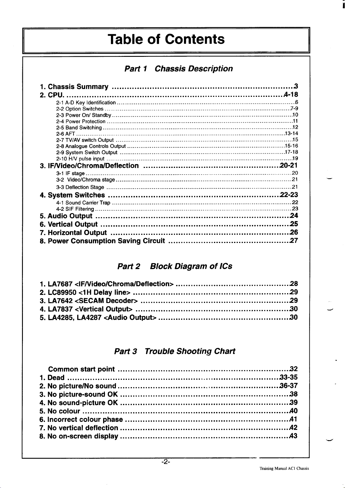
Table of Contents
Part 1 Chassis Description
i
1.
Chassis Summary
2.
3.
4.
5.
6.
7.
8.
. . ..................... ............................................................ ....
CPU
2.1 A. DKeyldentification ........ .. . .. .. ...... ........ ........ .. .. .. .. .. .. ......... ........ ........ .. .. ........ .. .......6
2.2 Option Switches ... .. .. .. .. ...... .. .. .................. .. .. .. .. .. ....... .. .. .. .. ...... .. .. .. . ......................7.9
2.3 Power On/ Standby ....... .. .. .. .. .. .. .. ................ .. .. .. . .. ........ .. .. .. .... ........ . .. .. ............ .. .. ...lO
2.4 Power Protection ...... ... . .. ........ .. .. .. .......... ... . .. .. .... .. ........... .. .. .. .. .. .. .. . .. ................ .....ll
2.5 Band Switching .. ...... .. .. .. ........... .. .. .... .. .. ... .. .. .. ....... .. .. ............. .. .. .. .. .. .. .. .. .. .. ....... .. ..l2
2.6 Am . .. .. .. .. .. .. .. .... .... ........... .. .. .. .. .... .. .. .......... .. .. .. .. .. .. . .............. .... .......... .. .. . .....l3.l4
2-7 TV/AV switch Output ... .. .. .. .... .. .. .. .............. .. .. .. .. .. .. ......... .. .. .. .. ...... .. .. .. . .......... .. .. .....l5
2.8 Analogue Controls Output .... .. . .. .. ................. .. ...... . .. .. ...... .. .. .. .. .. ........... .. .. .. ..........l5.l6
2-9 System Switch Output ... .. .. .. .. .. .. .. ................ .. .. .. .... .. .. .. ........... .. .. .. .. .. .. .. .... .. .. ......l7.l8
2-10 H/Vpulse input ... .... .. ... . .. ........ .. .......... ..... .. .. . .. .......... .. .. ............ .. .. . ............ .. .. .. ...l9
IF/Video/Chroma/Deflection
3-1 lFstage .......... . .. .. .. .... .. .. .. .. .. ............ .. .. .......... .. .. .... .......... . ... .. .. .. ........... .. ........ ...2O
3-2 Mdeo/Chroma stage . .. .. .. .. .. .. .. .. .. ................ .. .. .. .. . .. ...... .... .. ...... .. .. .. .. .. .. .. .. .. .. .........2l
3-3 Deflection Stage
System Switches
4-1 Sound Carrier Trap ..... .. .. . ............ .. ........ .. .. .. .. .. .. .. .. .. ..... .. .. .... .. .... .. .. .. . ............ .. .. ...22
4.2 SIFFiltering .. .. .. .. .. .. .... ............. .. .. ...... .. .. .. ........ .. .. .... .......... . .. .. ........ .. .... .. .. ....... ...23
Audio Output
Vertical Output
Horizontal Output
Power Consumption Saving Circuit
................... ..................................... ................
................ ........................ ... ...........
...... .. .. .. .. .... .. .. .................. .. .. .. .. ........... .. .. .... .... .. .. .. . ............ .. .. .. ..2l
................... .......... ........................ ...............
................. .. ............................... ........................ ...
....................... ............ ........................ ................
................... ...... ....... ......................... ..............
................................ ................
3
&-18
20-21
22-23
24
25
26
27
Part 2 Block Diagram of K%
1.
LA7687 clF/Video/Chroma/Deflection>
LC89950 <1H Delay line>
2.
LA7642 <SECAM Decoder>
3.
LA7837 cVertical Output>
4.
LA4285, LA4287 cAudio Output>
5.
.......................... ........................... .........
...................................... .......................
Part 3 Trouble Shooting Chart
Common start point
Dead
1.
No picture/No sound
2.
Uo picture-sound OK
3.
No sound-picture OK
4.
No colour
5.
ncorrect colour phase
6.
Uo vertical deflection
7.
Uo on-screen display
8.
.................... ............................... ........................... ......
....................... ............................... ......................... ...
................ ....... ... ........................ ..................
.............................. ....................... .. .........
............................. ........................... ...........
... .......................... .. ........................... .........
....................... ... .......................... .............
............................. ........................... ...........
............................. ........................... ...........
.................... .........................
.............................. .. ...........................
..... ......... .................................... ..30
33-35
36-37
28
29
29
30
.
32
38
39
Ao
Al
A2
A3
-2-
Training Manual AC 1 Chassis

Part 1 Chassis Description
1. Chassis Summary
The following figure shows a basic block diagram of the AC1 chassis. This chassis is constructed by the following ICS;
LC864508, IC801, for the CPU (system control circuit) for AC I -A chassis
LC864512, IC801, for the CPU (system control circuit) for AC1 -B chassis
LC864516, IC801, for the CPU (system control circuit) for AC1 -C chassis
LA7687, IC201, for the IF, video, chroma de-modulation and deflection circuit
LC89950, IC271, for the 1H delay line circuit
LA7642, IC280, for the SECAM decoder circuit
LA7837, IC501, for the vertical deflection output circuit
LA4287, ICOO1, for the audio output circuit, for AC1 -B chassis
LA4285, ICOO1, for the audio output circuit, for AC1 -A and AC1 -C chassis
ST24C02AB, etc., IC802, for the control memory IC
......
1-
L
Training Manual AC 1Chassis
..52n-m
......
%..s:=~=~~
SASSEX
1
AUDIOIN
ESTERNM AUDIOIN
.
.
-3-
t
—.
All
I
FOWR SUPWY
CIRCUIT
L
—
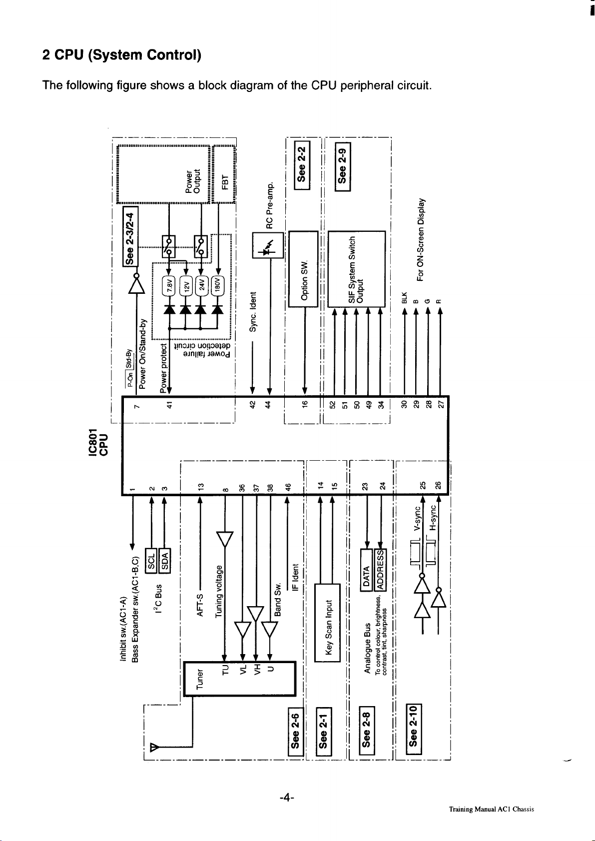
2 CPU (System Control)
The following figure shows a block diagram of the CPU peripheral circuit.
i
—.— .—-— -—. — -—-—
,,,,,
Ii
L
,,,,,
-—-— -- —-— -—-— ,
2
C/3
c
o
“E
o
T
+
MlII
Zz$?t%
i–.–
-il.–.–.–.-.i
I
Oalm
C-JOIN
i—-—-—-—-—-—-—- l, f—-—-lr-—-— -
I
cum
,-–;
J
L._-—-—.—.—.—-—-_-—; L.—.—.
I:m
di -
JI u
3
.2
c
ml
r%
G
x
—
II
ii
Ce
ii
&
a)
ii
r%
n
ii.
.—-—.
u-’
N’
—-— .—. J
-4-
Training Manual ACl Chassis

The following table shows pin descriptions of the CPU for AC1-A, AC1-B and ACI-C,
Pin Description
Pin Description
—
1
Inhibit output & Option switch
(AC1 -A)
Bass expander switch output &
Option switch (AC I -B, AC1 -C)
2 12Cbus SDA line 31
3 12Cbus SCL line
4 AV/SECAM switch output
5 Option switch (Tuner type)
6 Option switch (No. of positions)
(AC1 -A)
27 Red signal output for OSD
28 Green signal output for OSD
29 Blue signal output for OSD
30 Blanking signal output for OSD
Not used
32 Not used (AC1 -A, AC1 -B)
AV1/AV2 switch output (AC1 -C)
33 Not used (AC1 -A, AC1 -B)
Ignore input (AC1 -C)
34 Not used (AC1 -A)
Option switch (Blue back on/off) System switch output-VIF.M (AC1 -B,
(AC1-B)
L
Option switch (No. of positions& AV 35 AFT defeat switch output
modes) (AC1 -C)
7 Power& option switch (RC status)
8 Tuning voltage output
9 GND (Digital)
36 Band switch output 1-VHF Low
37 Band switch output 2-VHF High
38 Band switch output 3-UHF
39 Volume control output
AC1 -C)
10 Oscillator input for CPU 40 TV/AV switch output(TV:Low)
11
Oscillator output for CPU
12 +5 power supply (Digital)
13 AFT-S signal input
14 Key scan input (DC) 2
15 Key scan input (DC) 1
16 Option switch (Colour system)
17 Reset pulse input
18 Oscillator input for OSD
19 Oscillator output for OSD
20 Charge pump output
L
21 +5 power supply (Analogue)
41 Power error detection input
42 Sync identification input(No sync: Hi)
43 Colour killer input
44 RC signal input
45 SECAM killer input
46 IF identification input
47 Not used (AC1 -A, AC1 -B)
AV1 Start function input(ACl -C)
48 Option switch (No.of positions)
(AC1 -A)
Not used (AC1-B)
22 GND (Analogue) Option switch (No of positions & AV
23 Data-Analogue bus line
24 Address-Analogue bus line
25 Vertical pulse input
26 Horizontal pulse input
49 SIF system output-DK & option SW.
50 SIF system output-1 & option SW.
modes) & AV2 Start function
input(AC1-C)
51 SIF system output-BG & option SW.
52 SIF system output-M & option SW.
training Manual ACIChassis
“-s-

2-1 A-D Key Identification Circuit
The key identification circuit used in this chassis uses a switched resistive ladder network in
a A-D conversion circuit to generate and send a voltage to the CPU when a key is pressed.
The CPU uses this voltage to determine which key was pressed. This resistive circuit eliminates the need for encoder/decoder devices, simplifying design and adding to the reliability
of the TV.
The table shows the voltages input to CPU pin 14 and 15, when a given key is pressed.
K1 5“ ~
3-
CPU
+—
27k K2
10k
5.6k
&3
&
&
!W
KJ
27k
10k
5.6k
4
15
14
lrwut voltaqe to pin 15
Ke
K1
K2
K3
K4
K5
K6
K7
OFF
1
● Range of voltage
0.5V-1.1 V
l.l V- 1.7V
1.7V - 2.3V
2.3V - 3.OV
3.OU- 3.6V
3.6V - 4.2V
more than 4.2V
Less than 0.5V
3.9k
2.2k
L
2.7k K7
0.27k
—
Function
Position Up
Postion Up
Position Down
Level Up
Level Down
Undefined
Undefined
No Key pressed
~:j
~
~
K~
K~3
K~4
Ke
K8
-t
K9
KI O
K11
K12
K13
K14
OFF
3.9k
2.2k
2.7k
0.27k
7+
Intro It vnltarie to nin 14
.----- --..-=- .- . ... . .
* Range of voltage
0.5V-1.1 V
I.lv- 1.7V
1.7V - 2.3V
2.3V - 3.OV
3.OV- 3.6V
3.6V - 4.2V
more than 4.2V
Less than 0.5V
“ When the supply voltage is 5.OV.
Function
-rvlAv
TVIAV
SIF System
Colour System
Undefined
Preset
Function
No Key pressed
.
-6-
Training Manual AC 1 Chassis

2-2 Option switches
This chassis uses the option function switches to determine several different specifications
of the TV set.
The CPU determines the specification of TV by detecting the voltage level on option switches pins, pins, 1, 5, 6, 7, 16,49 to 52.
Following table shows the option functions and assigned pins of the CPU for each chassis.
Option functions
Inhibit
Bass expander
Type of tuner
No.s of positions
No.s of positions & AV modes
RC status
Blue back in
Colour system
SIF system
TV mode
Inhibit function (AC1-A chassis)
CPU
10
1
‘9
&lcl-A
pin 1
nla
pin 5
pins 6,48 nfa nla
nla
pin 7
nla
pin 16
pins 49-52 pins 49-52 pins 49-52
IN.SW
off
on
AC1-B AC1-C
nla nla
pin 1 pin 1
pin 5 pin 5
nla pins 6, 48
nla nla
pin 6 nla
pin 16 pin16
* n/a = not available
Specification
w/o Inhibit function
w/ Inhibit function
Buss
expander function ( AC1-B and AC1-C
chassis)
CPU
L
Rx
1
.
Type of tuner
‘9
EX.SW
off w/o Bass expander function
on
Specification
w/ Bass expander function
CPU
10
TU.SW
off Normal tuner
5
L
‘Y
on
Specification
CATV channel or hyper tuner
Training Manual AC I Chassis
-7-

Numbers of programme positions (AC1-A chassis)
i
CPU , 5“
48
9
10k
6
10k
poa
POS2 Sw
Posl Sw
‘ off
on
off
on
POS2 Sw
off 60 programme positions
off
on 100 programme positions
on 100 programme positions
k“
Numbers of programme positions and AV modes (AC1-C chassis)
CPU
6
48
5“
10k
$%A
10k
poa
POS2 Sw
Posl Sw
off
on
off
on
on
off
off
Specification
30 programme positions
Specification
60 programme positions
1 AV mode
100 programme positions
1 AV mode
100 programme positions
2 AV modes
100 programme positions
2 AV modes
Remote control status (AC1-A chassis)
CPU
Rx
7
‘9
Blue Back function in TV mode (AC1-B chassis)
CPU
RC SW. Specification
off
on
BL.SW
off
on
w/o remote control function
w/ remote control function
Specification
I
w/ Blue back function in TV mode
w/o Blue back function in TV mode
-8-
Training Manual AC1 Chassis

Colour system
CPU
J-1
SIF system
16
Rx
5V
10k
Pin16 Rx
more 4.53V
3.9V-4.53V
3.28V-3.9V 3.9k
2.66V-3.28V 6.8k
2.03V-2.66V
1.41V-2.03V 18k
0.78V-I .41V 33k
O.15V-O.78V
less O.15V
0.15K
1.8k
12k Multi-system(AC l-B/C)
10Ok PAL system
Open
Specification
Not used
Not used
Not used
China, Indonesia(ACl-B/C)
3 system
VMT system
PAL system
● When the supply voltage is 5.OV.
I
11.sw
BG.SW I.sw
off
off off on
off off on
on
on
off
off on on
on
off
on on on
off
off
off on
on off off
on
in on on
off
off
off
DK.SW
off Multi-system
off
on
off 3 system
off
off
off China 3
on
Specification
Px
Indonesia 1
East Europe
China 1
China 2
Indonesia 2
No system
J7
(ACI -A)
(ACI-A)
(AC1 -A)
Training Manual AC I Chassis
-9-
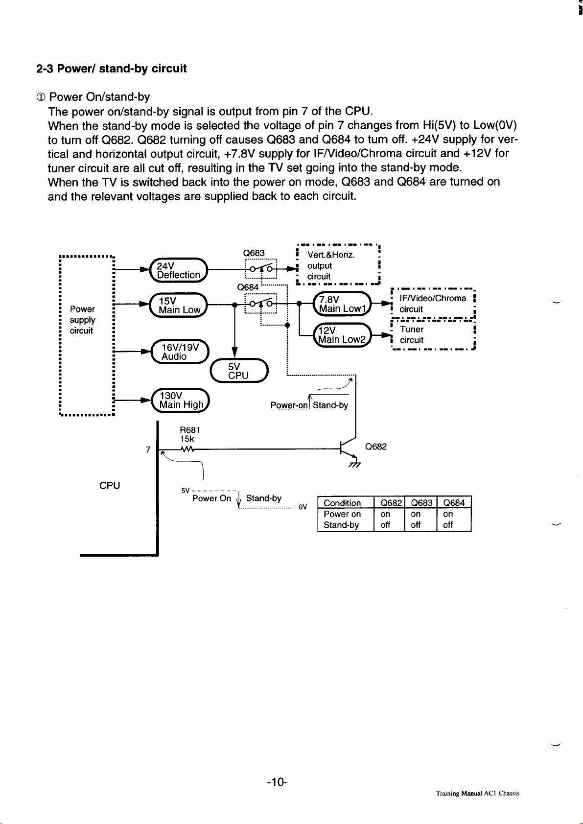
2-3 Power/ stand-by circuit
O Power On/stand-by
The power on/stand-by signal is output from pin 7 of the CPU.
When the stand-by mode is selected the voltage of pin 7 changes from Hi(5V) to Low(OV)
to turn off Q682. Q682 turning off causes Q683 and Q684 to turn off. +24V supply for vertical and horizontal output circuit, +7.8V supply for lF/Video/Chroma circuit and +12V for
tuner circuit are all cut off, resulting in the TV set going into the stand-by mode.
When the TV is switched back into the power on mode, Q683 and Q684 are turned on
and the relevant voltages are supplied back to each circuit.
,-.,-.,-.,-. .. . ..
● mmmmmmm. mmm mm.
.
.
.
.
.
.
.
.
.
.
.
.
.
.
.
.
.
.
.
.
.
Q683
ii
supply :
:
.
:
.
.
.
.
.
.
.
.
.
.
.
.
.
.
.
.
CPU
...................................
R681
15k
7
AAA
7
5v --------
Power On
t
““sEd’by-””-”’”o’ ~
Q682
-1o-
Traming Manual AC I Chassis

ii
2-4 Protection circuit
L
This chassis employs two kinds of protection circuit, one controlled by software through the
CPU and the other by hardware.
Protection circuit (software)
The protection circuit is provided to disable the operation of the TV set in case of a circuit
malfunction.
When an abnormality occurs during TV reception it causes pin 41 of the CPU to go continually Low (less than 0.8V) for about one second. The CPU detects that this has
occurred and outputs the signal to cut off Q683 and Q684.
Protection circuit (hardware)
When a power failure is detected by diodes D643, D644 and D645, this protection circuit
operates causing the power oscillation to stop.
If one of the above diodes is turned on, the voltage of Q631 -emitter decreases, and it
turns on completely. Photo-coupler D615 is driven by this and generates a current which
drives Q612 on. As a result, the operation of the power oscillation circuit is stopped.
Under normal circumstances these parts, D615, Q631, D641, R635, R636, VR631 are
operating as the error detection and regulation circuit for +130V power supply.
D445
D201 ,
D492
I
● mmmmmmmmmmmmmd
.
i
.
.
■
✎
■
✎
✎
✎
✎
✎
✎
Power
✎
✎
✎
supply
✎
✎
✎
circuit
✎
✎
✎
L
✎
✎
✎
✎
✎
✎
✎
✎
✎
✎
✎
.
.
.
.
.
.
+...
mmmm. mmm. m
.
.
.
.
.
.
.
.
.
.
.
.
.
.
.
.
.
.
.
.
.
.
.
.
.
.
.
.
. [ 1/ I
.
.
.
.
.
.
(
CPU
41
Protect
(2683
................
*@;
................
.. . . . . .
Q684 . “--’ --’--’=-’-J ,
................ I
+-@ ~
D655 ;
..... . . . . ..
R635
VR631
Rf=$ :$\ :
h
130V
Regulator
circuit
Power 7
R681
15k
iAA
, -.,-.,-.! -. 0-..,
t
! Vert.&Horiz.
& output
- circuit
ADfj41 E
)
_ power
=a
;
i
‘j
.... . . . . ........,,. ...
Power
oscillation
circuit
P................*. . . . . . . . . . . ..
operation ~ failuer
Heater
5V
180V
Jlllll18!o.slllllll.!lL
FBT j
:,,,,,...,,,,,,.,,..,,,,,..%
., -.,-.,-., -- i---
L1
- lF/Video/Chroma R
.- . .- 1-------- ,.1
.m-. a-. .-. m-. *-. .
“m-, --}.-,.- ,.-,4
as...,,,,
.
.
.
.
.
.
.
.
.
■
:
.
I
:
i
Training Manual AC 1Chassis
-11-

2-5 Band switching circuit
The band switching control signals are output from pins 36, 37 and 38 of the CPU and fed
to the base of Q1 03, Q104 and Q1 05, band switching transistors.
The one of these transistors then supplies the drive voltage(+l 2V) to the tuner according to
the output signal from the CPU as shown below table.
Antenna
Tuner
i
I._
Cllo3
●
VL
Q104
●
VH
Q105
●
u
Band Switching Logic
output
Pin36 Pin 37 Pin 38
LH
HL
HHL
H on
H off
Q103 Q104
off off
on off
off
off
Q105
on
12k
12k
R898
12k
Selected Band
VHF-Low
VHF-High
UHF
36 VL
37 VH
38 UHF
CPU
-12-
Tmining Manual AC1 Chassis
2-6 AFT
This chassis employs two kinds of the AFT circuit, it’s called the Digital AFT and the Trace
AFT.
The digital AFT operates as the hardware AFT in the tuner circuit. Every channel selection,
the CPU reads out the tuning data from the memory and then changes tuning voltage output
from pin 8 to obtain the best tuned picture.
The trace AFT is to prevent the drifting of receiving condition caused by the temperature
etc. The CPU monitors the AFT S-curve signal input to pin 13 and maintains the correct
tuned picture by controlling the output tuning voltage.
.
Digital An
(1)
The CPU outputs tuning voltage(Start value) which is subtracted with the step as table-1
from the stored tuning voltage data in the memory and waits for 240ms.
II* When the AFT voltage is less than 1.5V, go to step (4).
III* Other than the above, go to step (2).
Increase the tuning voltage along with table-2a until the AFT voltage reaches less than
‘w
(2)
1.5V. Go to next step.
Decrease the tuning voltage along with table-2b until the AFT voltage reaches more than
(3)
2.OV. Go to next step.
The CPU judges that the sync. signal is existing or not by detecting the voltage on pin
(4)
46,
If the CPU detects a low voltage on pin 46, go to step (2).
If the CPU detects a high(5V) voltage on pin 46, complete the digital AFT operation and
go to the Trace AFT stage.
Trace Am
After completing the digital AFT operation, the CPU switches to the trace AFT mode.
(1)
If the AFT v;ltage ii more than 3.OV and the IF ident. signal is detected, the CPU
increases the tuning voltage along with table-3.
(2)
If the AFT voltage is less than 2.OV and the IF ident. signal is detected, the CPU
decreases the tuning voltage along with table-3.
‘L
In the preset mode and fine tuning mode, this function does not operate.
(3)
‘“L
Tablel Substructed steps
~=
Table-2 Tuning apeed of digital AFT
(a) Highspead (steps/10msec.)
~
(b) Mid spead (steps/10msec.)
~
Training Manual AC I Chassis
Table-3 Tuning spesd of Trace AFT
-13-

Tuning
Tuner
TU
Q184
‘ 8
TUNING OUT
F
CPU
IF IDENT IN
AFTIN 13
46 w
4
J? $:”
l\
R858
150
R177
120k
R176
39k
RI 75
82k
IC201
lF&VIDEO
2 IF IDENT
7 AFT
I
J? %::
Input Signal
Pin 13
of IC801
Pin 8
of IC801
Pin 46
of IC801
AFT S-Curve
Input
Tuning Voltage
IF Ident.
Signal Input
-,:!
!,,
Input Voltage Level of Pin 13
LL(OV-1.5V)
L (1.5V-2.OV)
M (2.O-3.OV)
H (3.OV-3.5V)
HH(3.5V-5V)
‘ Tuned point
Judgement
Tuning Voltage Down
Tuning Voltage
Tuned Centre
Tuning Voltage Up
Tuning Voltage Up
Down
3.5V
3.OV
A
2.OV
-14-
Training Manual AC 1 Chassis