

Page 1

COLOUR TELEVISION
TRAINING MANUAL
FILE NO. c-?/Ps60-uo /
I
Chassis Series ACI-A
ACI-B
ACI-C
CIRCUIT DESCRIPTION
BLOCK DIAGRAM OF
TROUBLE SHOOTING
/~S
I
REFERENCE NO. T1520009
Page 2
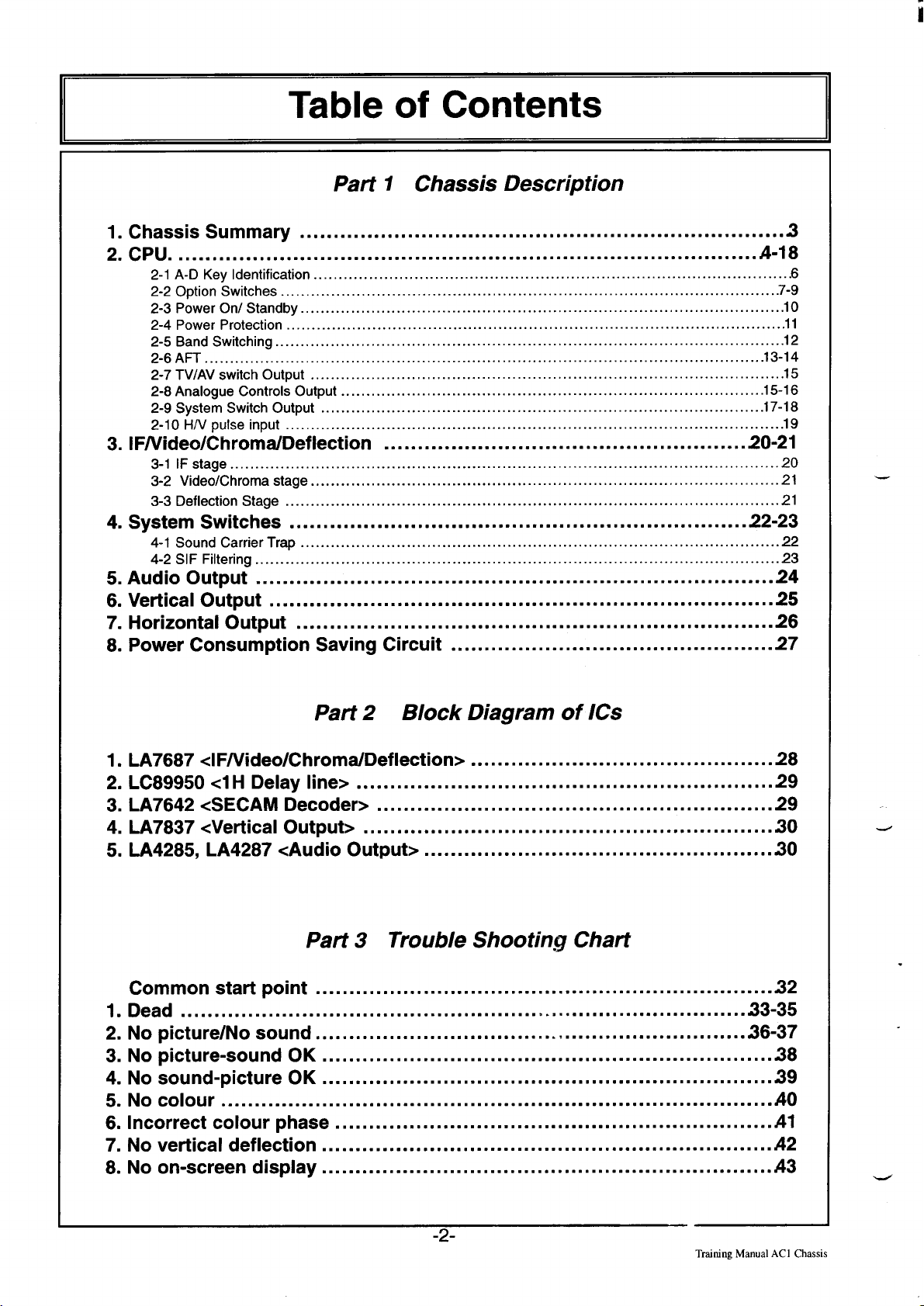
Table of Contents
Part 1 Chassis Description
i
1.
Chassis Summary
2.
3.
4.
5.
6.
7.
8.
. . ..................... ............................................................ ....
CPU
2.1 A. DKeyldentification ........ .. . .. .. ...... ........ ........ .. .. .. .. .. .. ......... ........ ........ .. .. ........ .. .......6
2.2 Option Switches ... .. .. .. .. ...... .. .. .................. .. .. .. .. .. ....... .. .. .. .. ...... .. .. .. . ......................7.9
2.3 Power On/ Standby ....... .. .. .. .. .. .. .. ................ .. .. .. . .. ........ .. .. .. .... ........ . .. .. ............ .. .. ...lO
2.4 Power Protection ...... ... . .. ........ .. .. .. .......... ... . .. .. .... .. ........... .. .. .. .. .. .. .. . .. ................ .....ll
2.5 Band Switching .. ...... .. .. .. ........... .. .. .... .. .. ... .. .. .. ....... .. .. ............. .. .. .. .. .. .. .. .. .. .. ....... .. ..l2
2.6 Am . .. .. .. .. .. .. .. .... .... ........... .. .. .. .. .... .. .. .......... .. .. .. .. .. .. . .............. .... .......... .. .. . .....l3.l4
2-7 TV/AV switch Output ... .. .. .. .... .. .. .. .............. .. .. .. .. .. .. ......... .. .. .. .. ...... .. .. .. . .......... .. .. .....l5
2.8 Analogue Controls Output .... .. . .. .. ................. .. ...... . .. .. ...... .. .. .. .. .. ........... .. .. .. ..........l5.l6
2-9 System Switch Output ... .. .. .. .. .. .. .. ................ .. .. .. .... .. .. .. ........... .. .. .. .. .. .. .. .... .. .. ......l7.l8
2-10 H/Vpulse input ... .... .. ... . .. ........ .. .......... ..... .. .. . .. .......... .. .. ............ .. .. . ............ .. .. .. ...l9
IF/Video/Chroma/Deflection
3-1 lFstage .......... . .. .. .. .... .. .. .. .. .. ............ .. .. .......... .. .. .... .......... . ... .. .. .. ........... .. ........ ...2O
3-2 Mdeo/Chroma stage . .. .. .. .. .. .. .. .. .. ................ .. .. .. .. . .. ...... .... .. ...... .. .. .. .. .. .. .. .. .. .. .........2l
3-3 Deflection Stage
System Switches
4-1 Sound Carrier Trap ..... .. .. . ............ .. ........ .. .. .. .. .. .. .. .. .. ..... .. .. .... .. .... .. .. .. . ............ .. .. ...22
4.2 SIFFiltering .. .. .. .. .. .. .... ............. .. .. ...... .. .. .. ........ .. .. .... .......... . .. .. ........ .. .... .. .. ....... ...23
Audio Output
Vertical Output
Horizontal Output
Power Consumption Saving Circuit
................... ..................................... ................
................ ........................ ... ...........
...... .. .. .. .. .... .. .. .................. .. .. .. .. ........... .. .. .... .... .. .. .. . ............ .. .. .. ..2l
................... .......... ........................ ...............
................. .. ............................... ........................ ...
....................... ............ ........................ ................
................... ...... ....... ......................... ..............
................................ ................
3
&-18
20-21
22-23
24
25
26
27
Part 2 Block Diagram of K%
1.
LA7687 clF/Video/Chroma/Deflection>
LC89950 <1H Delay line>
2.
LA7642 <SECAM Decoder>
3.
LA7837 cVertical Output>
4.
LA4285, LA4287 cAudio Output>
5.
.......................... ........................... .........
...................................... .......................
Part 3 Trouble Shooting Chart
Common start point
Dead
1.
No picture/No sound
2.
Uo picture-sound OK
3.
No sound-picture OK
4.
No colour
5.
ncorrect colour phase
6.
Uo vertical deflection
7.
Uo on-screen display
8.
.................... ............................... ........................... ......
....................... ............................... ......................... ...
................ ....... ... ........................ ..................
.............................. ....................... .. .........
............................. ........................... ...........
... .......................... .. ........................... .........
....................... ... .......................... .............
............................. ........................... ...........
............................. ........................... ...........
.................... .........................
.............................. .. ...........................
..... ......... .................................... ..30
33-35
36-37
28
29
29
30
.
32
38
39
Ao
Al
A2
A3
-2-
Training Manual AC 1 Chassis
Page 3

Part 1 Chassis Description
1. Chassis Summary
The following figure shows a basic block diagram of the AC1 chassis. This chassis is constructed by the following ICS;
LC864508, IC801, for the CPU (system control circuit) for AC I -A chassis
LC864512, IC801, for the CPU (system control circuit) for AC1 -B chassis
LC864516, IC801, for the CPU (system control circuit) for AC1 -C chassis
LA7687, IC201, for the IF, video, chroma de-modulation and deflection circuit
LC89950, IC271, for the 1H delay line circuit
LA7642, IC280, for the SECAM decoder circuit
LA7837, IC501, for the vertical deflection output circuit
LA4287, ICOO1, for the audio output circuit, for AC1 -B chassis
LA4285, ICOO1, for the audio output circuit, for AC1 -A and AC1 -C chassis
ST24C02AB, etc., IC802, for the control memory IC
......
1-
L
Training Manual AC 1Chassis
..52n-m
......
%..s:=~=~~
SASSEX
1
AUDIOIN
ESTERNM AUDIOIN
.
.
-3-
t
—.
All
I
FOWR SUPWY
CIRCUIT
L
—
Page 4
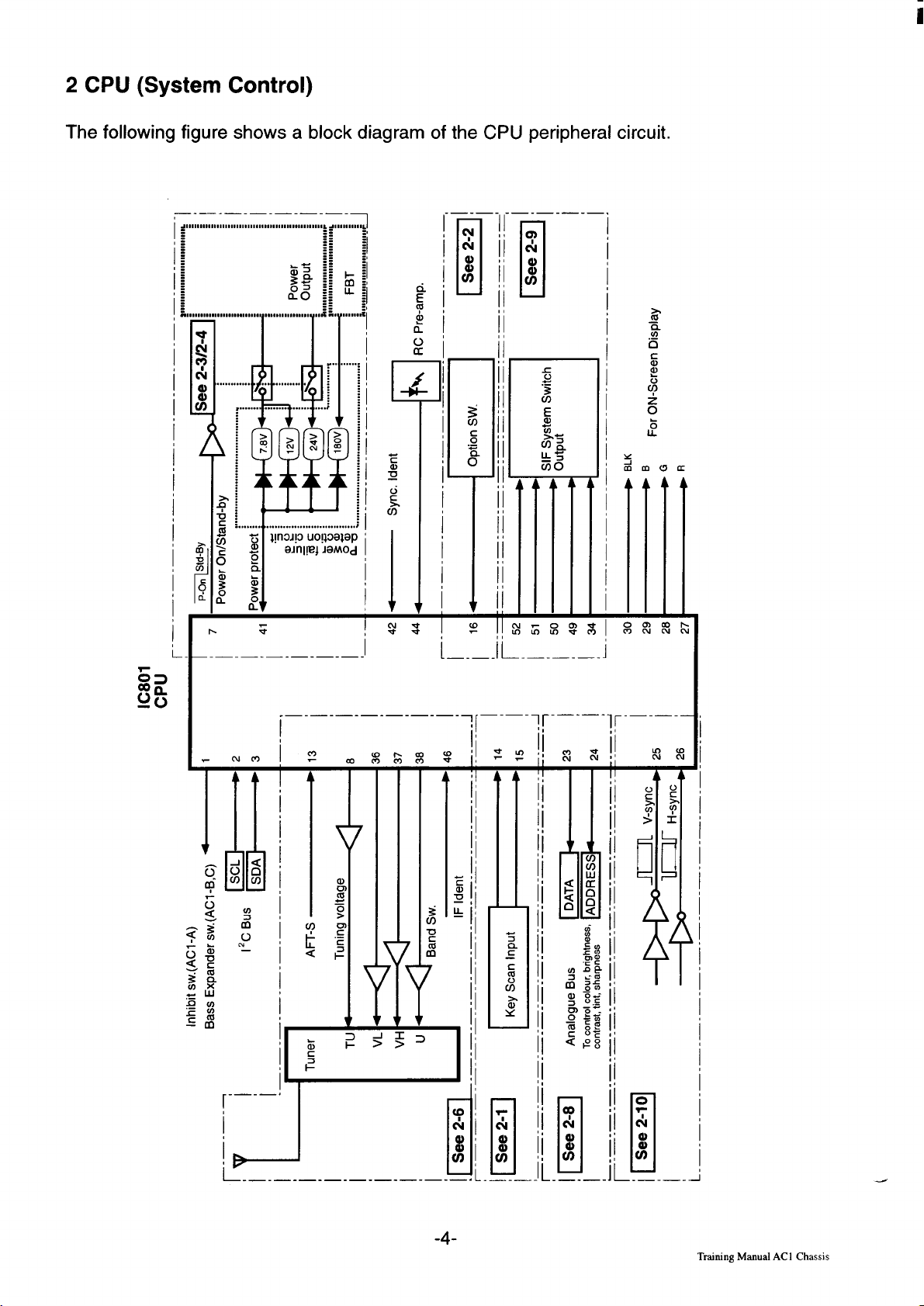
2 CPU (System Control)
The following figure shows a block diagram of the CPU peripheral circuit.
i
—.— .—-— -—. — -—-—
,,,,,
Ii
L
,,,,,
-—-— -- —-— -—-— ,
2
C/3
c
o
“E
o
T
+
MlII
Zz$?t%
i–.–
-il.–.–.–.-.i
I
Oalm
C-JOIN
i—-—-—-—-—-—-—- l, f—-—-lr-—-— -
I
cum
,-–;
J
L._-—-—.—.—.—-—-_-—; L.—.—.
I:m
di -
JI u
3
.2
c
ml
r%
G
x
—
II
ii
Ce
ii
&
a)
ii
r%
n
ii.
.—-—.
u-’
N’
—-— .—. J
-4-
Training Manual ACl Chassis
Page 5

The following table shows pin descriptions of the CPU for AC1-A, AC1-B and ACI-C,
Pin Description
Pin Description
—
1
Inhibit output & Option switch
(AC1 -A)
Bass expander switch output &
Option switch (AC I -B, AC1 -C)
2 12Cbus SDA line 31
3 12Cbus SCL line
4 AV/SECAM switch output
5 Option switch (Tuner type)
6 Option switch (No. of positions)
(AC1 -A)
27 Red signal output for OSD
28 Green signal output for OSD
29 Blue signal output for OSD
30 Blanking signal output for OSD
Not used
32 Not used (AC1 -A, AC1 -B)
AV1/AV2 switch output (AC1 -C)
33 Not used (AC1 -A, AC1 -B)
Ignore input (AC1 -C)
34 Not used (AC1 -A)
Option switch (Blue back on/off) System switch output-VIF.M (AC1 -B,
(AC1-B)
L
Option switch (No. of positions& AV 35 AFT defeat switch output
modes) (AC1 -C)
7 Power& option switch (RC status)
8 Tuning voltage output
9 GND (Digital)
36 Band switch output 1-VHF Low
37 Band switch output 2-VHF High
38 Band switch output 3-UHF
39 Volume control output
AC1 -C)
10 Oscillator input for CPU 40 TV/AV switch output(TV:Low)
11
Oscillator output for CPU
12 +5 power supply (Digital)
13 AFT-S signal input
14 Key scan input (DC) 2
15 Key scan input (DC) 1
16 Option switch (Colour system)
17 Reset pulse input
18 Oscillator input for OSD
19 Oscillator output for OSD
20 Charge pump output
L
21 +5 power supply (Analogue)
41 Power error detection input
42 Sync identification input(No sync: Hi)
43 Colour killer input
44 RC signal input
45 SECAM killer input
46 IF identification input
47 Not used (AC1 -A, AC1 -B)
AV1 Start function input(ACl -C)
48 Option switch (No.of positions)
(AC1 -A)
Not used (AC1-B)
22 GND (Analogue) Option switch (No of positions & AV
23 Data-Analogue bus line
24 Address-Analogue bus line
25 Vertical pulse input
26 Horizontal pulse input
49 SIF system output-DK & option SW.
50 SIF system output-1 & option SW.
modes) & AV2 Start function
input(AC1-C)
51 SIF system output-BG & option SW.
52 SIF system output-M & option SW.
training Manual ACIChassis
“-s-
Page 6

2-1 A-D Key Identification Circuit
The key identification circuit used in this chassis uses a switched resistive ladder network in
a A-D conversion circuit to generate and send a voltage to the CPU when a key is pressed.
The CPU uses this voltage to determine which key was pressed. This resistive circuit eliminates the need for encoder/decoder devices, simplifying design and adding to the reliability
of the TV.
The table shows the voltages input to CPU pin 14 and 15, when a given key is pressed.
K1 5“ ~
3-
CPU
+—
27k K2
10k
5.6k
&3
&
&
!W
KJ
27k
10k
5.6k
4
15
14
lrwut voltaqe to pin 15
Ke
K1
K2
K3
K4
K5
K6
K7
OFF
1
● Range of voltage
0.5V-1.1 V
l.l V- 1.7V
1.7V - 2.3V
2.3V - 3.OV
3.OU- 3.6V
3.6V - 4.2V
more than 4.2V
Less than 0.5V
3.9k
2.2k
L
2.7k K7
0.27k
—
Function
Position Up
Postion Up
Position Down
Level Up
Level Down
Undefined
Undefined
No Key pressed
~:j
~
~
K~
K~3
K~4
Ke
K8
-t
K9
KI O
K11
K12
K13
K14
OFF
3.9k
2.2k
2.7k
0.27k
7+
Intro It vnltarie to nin 14
.----- --..-=- .- . ... . .
* Range of voltage
0.5V-1.1 V
I.lv- 1.7V
1.7V - 2.3V
2.3V - 3.OV
3.OV- 3.6V
3.6V - 4.2V
more than 4.2V
Less than 0.5V
“ When the supply voltage is 5.OV.
Function
-rvlAv
TVIAV
SIF System
Colour System
Undefined
Preset
Function
No Key pressed
.
-6-
Training Manual AC 1 Chassis
Page 7

2-2 Option switches
This chassis uses the option function switches to determine several different specifications
of the TV set.
The CPU determines the specification of TV by detecting the voltage level on option switches pins, pins, 1, 5, 6, 7, 16,49 to 52.
Following table shows the option functions and assigned pins of the CPU for each chassis.
Option functions
Inhibit
Bass expander
Type of tuner
No.s of positions
No.s of positions & AV modes
RC status
Blue back in
Colour system
SIF system
TV mode
Inhibit function (AC1-A chassis)
CPU
10
1
‘9
&lcl-A
pin 1
nla
pin 5
pins 6,48 nfa nla
nla
pin 7
nla
pin 16
pins 49-52 pins 49-52 pins 49-52
IN.SW
off
on
AC1-B AC1-C
nla nla
pin 1 pin 1
pin 5 pin 5
nla pins 6, 48
nla nla
pin 6 nla
pin 16 pin16
* n/a = not available
Specification
w/o Inhibit function
w/ Inhibit function
Buss
expander function ( AC1-B and AC1-C
chassis)
CPU
L
Rx
1
.
Type of tuner
‘9
EX.SW
off w/o Bass expander function
on
Specification
w/ Bass expander function
CPU
10
TU.SW
off Normal tuner
5
L
‘Y
on
Specification
CATV channel or hyper tuner
Training Manual AC I Chassis
-7-
Page 8

Numbers of programme positions (AC1-A chassis)
i
CPU , 5“
48
9
10k
6
10k
poa
POS2 Sw
Posl Sw
‘ off
on
off
on
POS2 Sw
off 60 programme positions
off
on 100 programme positions
on 100 programme positions
k“
Numbers of programme positions and AV modes (AC1-C chassis)
CPU
6
48
5“
10k
$%A
10k
poa
POS2 Sw
Posl Sw
off
on
off
on
on
off
off
Specification
30 programme positions
Specification
60 programme positions
1 AV mode
100 programme positions
1 AV mode
100 programme positions
2 AV modes
100 programme positions
2 AV modes
Remote control status (AC1-A chassis)
CPU
Rx
7
‘9
Blue Back function in TV mode (AC1-B chassis)
CPU
RC SW. Specification
off
on
BL.SW
off
on
w/o remote control function
w/ remote control function
Specification
I
w/ Blue back function in TV mode
w/o Blue back function in TV mode
-8-
Training Manual AC1 Chassis
Page 9

Colour system
CPU
J-1
SIF system
16
Rx
5V
10k
Pin16 Rx
more 4.53V
3.9V-4.53V
3.28V-3.9V 3.9k
2.66V-3.28V 6.8k
2.03V-2.66V
1.41V-2.03V 18k
0.78V-I .41V 33k
O.15V-O.78V
less O.15V
0.15K
1.8k
12k Multi-system(AC l-B/C)
10Ok PAL system
Open
Specification
Not used
Not used
Not used
China, Indonesia(ACl-B/C)
3 system
VMT system
PAL system
● When the supply voltage is 5.OV.
I
11.sw
BG.SW I.sw
off
off off on
off off on
on
on
off
off on on
on
off
on on on
off
off
off on
on off off
on
in on on
off
off
off
DK.SW
off Multi-system
off
on
off 3 system
off
off
off China 3
on
Specification
Px
Indonesia 1
East Europe
China 1
China 2
Indonesia 2
No system
J7
(ACI -A)
(ACI-A)
(AC1 -A)
Training Manual AC I Chassis
-9-
Page 10
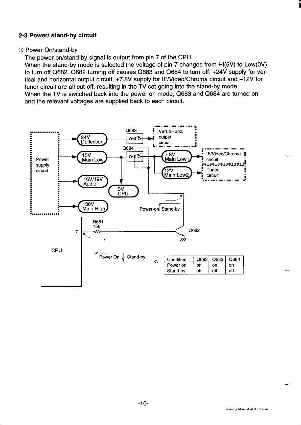
2-3 Power/ stand-by circuit
O Power On/stand-by
The power on/stand-by signal is output from pin 7 of the CPU.
When the stand-by mode is selected the voltage of pin 7 changes from Hi(5V) to Low(OV)
to turn off Q682. Q682 turning off causes Q683 and Q684 to turn off. +24V supply for vertical and horizontal output circuit, +7.8V supply for lF/Video/Chroma circuit and +12V for
tuner circuit are all cut off, resulting in the TV set going into the stand-by mode.
When the TV is switched back into the power on mode, Q683 and Q684 are turned on
and the relevant voltages are supplied back to each circuit.
,-.,-.,-.,-. .. . ..
● mmmmmmm. mmm mm.
.
.
.
.
.
.
.
.
.
.
.
.
.
.
.
.
.
.
.
.
.
Q683
ii
supply :
:
.
:
.
.
.
.
.
.
.
.
.
.
.
.
.
.
.
.
CPU
...................................
R681
15k
7
AAA
7
5v --------
Power On
t
““sEd’by-””-”’”o’ ~
Q682
-1o-
Traming Manual AC I Chassis
Page 11

ii
2-4 Protection circuit
L
This chassis employs two kinds of protection circuit, one controlled by software through the
CPU and the other by hardware.
Protection circuit (software)
The protection circuit is provided to disable the operation of the TV set in case of a circuit
malfunction.
When an abnormality occurs during TV reception it causes pin 41 of the CPU to go continually Low (less than 0.8V) for about one second. The CPU detects that this has
occurred and outputs the signal to cut off Q683 and Q684.
Protection circuit (hardware)
When a power failure is detected by diodes D643, D644 and D645, this protection circuit
operates causing the power oscillation to stop.
If one of the above diodes is turned on, the voltage of Q631 -emitter decreases, and it
turns on completely. Photo-coupler D615 is driven by this and generates a current which
drives Q612 on. As a result, the operation of the power oscillation circuit is stopped.
Under normal circumstances these parts, D615, Q631, D641, R635, R636, VR631 are
operating as the error detection and regulation circuit for +130V power supply.
D445
D201 ,
D492
I
● mmmmmmmmmmmmmd
.
i
.
.
■
✎
■
✎
✎
✎
✎
✎
✎
Power
✎
✎
✎
supply
✎
✎
✎
circuit
✎
✎
✎
L
✎
✎
✎
✎
✎
✎
✎
✎
✎
✎
✎
.
.
.
.
.
.
+...
mmmm. mmm. m
.
.
.
.
.
.
.
.
.
.
.
.
.
.
.
.
.
.
.
.
.
.
.
.
.
.
.
.
. [ 1/ I
.
.
.
.
.
.
(
CPU
41
Protect
(2683
................
*@;
................
.. . . . . .
Q684 . “--’ --’--’=-’-J ,
................ I
+-@ ~
D655 ;
..... . . . . ..
R635
VR631
Rf=$ :$\ :
h
130V
Regulator
circuit
Power 7
R681
15k
iAA
, -.,-.,-.! -. 0-..,
t
! Vert.&Horiz.
& output
- circuit
ADfj41 E
)
_ power
=a
;
i
‘j
.... . . . . ........,,. ...
Power
oscillation
circuit
P................*. . . . . . . . . . . ..
operation ~ failuer
Heater
5V
180V
Jlllll18!o.slllllll.!lL
FBT j
:,,,,,...,,,,,,.,,..,,,,,..%
., -.,-.,-., -- i---
L1
- lF/Video/Chroma R
.- . .- 1-------- ,.1
.m-. a-. .-. m-. *-. .
“m-, --}.-,.- ,.-,4
as...,,,,
.
.
.
.
.
.
.
.
.
■
:
.
I
:
i
Training Manual AC 1Chassis
-11-
Page 12

2-5 Band switching circuit
The band switching control signals are output from pins 36, 37 and 38 of the CPU and fed
to the base of Q1 03, Q104 and Q1 05, band switching transistors.
The one of these transistors then supplies the drive voltage(+l 2V) to the tuner according to
the output signal from the CPU as shown below table.
Antenna
Tuner
i
I._
Cllo3
●
VL
Q104
●
VH
Q105
●
u
Band Switching Logic
output
Pin36 Pin 37 Pin 38
LH
HL
HHL
H on
H off
Q103 Q104
off off
on off
off
off
Q105
on
12k
12k
R898
12k
Selected Band
VHF-Low
VHF-High
UHF
36 VL
37 VH
38 UHF
CPU
-12-
Tmining Manual AC1 Chassis
Page 13
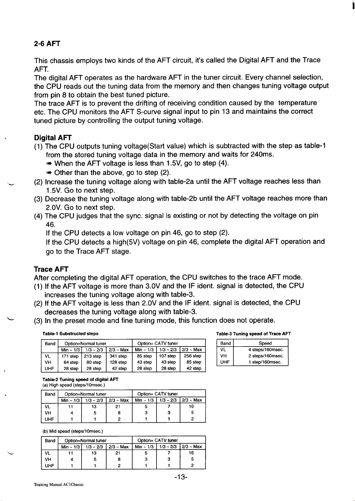
2-6 AFT
This chassis employs two kinds of the AFT circuit, it’s called the Digital AFT and the Trace
AFT.
The digital AFT operates as the hardware AFT in the tuner circuit. Every channel selection,
the CPU reads out the tuning data from the memory and then changes tuning voltage output
from pin 8 to obtain the best tuned picture.
The trace AFT is to prevent the drifting of receiving condition caused by the temperature
etc. The CPU monitors the AFT S-curve signal input to pin 13 and maintains the correct
tuned picture by controlling the output tuning voltage.
.
Digital An
(1)
The CPU outputs tuning voltage(Start value) which is subtracted with the step as table-1
from the stored tuning voltage data in the memory and waits for 240ms.
II* When the AFT voltage is less than 1.5V, go to step (4).
III* Other than the above, go to step (2).
Increase the tuning voltage along with table-2a until the AFT voltage reaches less than
‘w
(2)
1.5V. Go to next step.
Decrease the tuning voltage along with table-2b until the AFT voltage reaches more than
(3)
2.OV. Go to next step.
The CPU judges that the sync. signal is existing or not by detecting the voltage on pin
(4)
46,
If the CPU detects a low voltage on pin 46, go to step (2).
If the CPU detects a high(5V) voltage on pin 46, complete the digital AFT operation and
go to the Trace AFT stage.
Trace Am
After completing the digital AFT operation, the CPU switches to the trace AFT mode.
(1)
If the AFT v;ltage ii more than 3.OV and the IF ident. signal is detected, the CPU
increases the tuning voltage along with table-3.
(2)
If the AFT voltage is less than 2.OV and the IF ident. signal is detected, the CPU
decreases the tuning voltage along with table-3.
‘L
In the preset mode and fine tuning mode, this function does not operate.
(3)
‘“L
Tablel Substructed steps
~=
Table-2 Tuning apeed of digital AFT
(a) Highspead (steps/10msec.)
~
(b) Mid spead (steps/10msec.)
~
Training Manual AC I Chassis
Table-3 Tuning spesd of Trace AFT
-13-
Page 14

Tuning
Tuner
TU
Q184
‘ 8
TUNING OUT
F
CPU
IF IDENT IN
AFTIN 13
46 w
4
J? $:”
l\
R858
150
R177
120k
R176
39k
RI 75
82k
IC201
lF&VIDEO
2 IF IDENT
7 AFT
I
J? %::
Input Signal
Pin 13
of IC801
Pin 8
of IC801
Pin 46
of IC801
AFT S-Curve
Input
Tuning Voltage
IF Ident.
Signal Input
-,:!
!,,
Input Voltage Level of Pin 13
LL(OV-1.5V)
L (1.5V-2.OV)
M (2.O-3.OV)
H (3.OV-3.5V)
HH(3.5V-5V)
‘ Tuned point
Judgement
Tuning Voltage Down
Tuning Voltage
Tuned Centre
Tuning Voltage Up
Tuning Voltage Up
Down
3.5V
3.OV
A
2.OV
-14-
Training Manual AC 1 Chassis
Page 15

2-7 TV/AV switching circuit
The TV/AV switching signal output from pin 40 of the CPU is supplied to pin 4 of ICOO1,
audio output, and pin 1 of IC201 to select the internal or external source. The SECAM
switching signal output from pin 4 is sent to pin 1 of IC201. The output of each mode and
system is shown in the table below.
CPU
AV/SECA;
TVIAV
40
R803
5.6k
R815 R804
680
-“4
15k
To SECAM IC
pin12
L
R861
5.6k
5V
d?
OUTPUT PAUNTSC SECAM
pin 4
40 L L
Din
Hz L Hz
I
I
Q016
RI 71
lk
“1
TV I Av I
Icool
AUDIO OUTPUT
4 lNT./EXT. SW.
IC201
lV/VIDEO
1 AVISECAM
SIF IN
PAUNTSC SECAM
H
H H
● Hz= High impedance
2-8 Analogue control circuit
The colour saturation, brightness, contrast, tint, and sharpness for picture controls and
selection of crystal control are controlled via the analogue bus lines connected from pins 23
and 24 of the CPU to pins 18 and 19 of IC201, LA7687. The CPU outputs the data and
L
address signals during a vertical retracing period, and the control address and data of crystal are represented in 8 bits and data of picture controls are represented in 7 bits.
The timing charts and specifications of bus lines are described on next page.
The sound volume control is output from pin 39 as 7 bits PWM (Pulse Width Modulation)
signal. This signal is applied to the audio output IC as DC control voltage through the filter-
ing circuit
IC201
CPU
\
DATA
ADDRESS
R219
220
R218
lk
I
23
24
39
lF/VIDEO
19 Data
18 Address
Icool
AUDIO OUTPUT
‘L
VOLUME
Filtering
circuit
*
5 VOL
-15-
Traming Manual AC I Chassis
Page 16

Output Value
(1) Address voltaae (8 bits= 255 steDs)
.,
“. ,,
Control Item Specification of
LA7687
Crystal O- O.17V
Brightness 0.77V - 1.OIV
Contrast
Colour
Sharpness 3.50V - 3.74V
Tint 4.40V - 5.00V
1
1.68V -1 .93V
2.59V - 2.83V
(2) Data voltage
a) Crystal (8 bits= 255 steps)
Control Item Specification of
LA7687 voltage of CPU
PAL4.43
I
PAL3.58
NTSC3.58 2.90V - 3.90V
NTSC4.43 4.1 Ov - 5.00V
O - 1.48V 0.04V (02/255)
1.70V - 2.70V
Reference output
voltage of CPU
O.oiv (02/255)
0.86V (44/255)
1.76V
2.67V (136/255)
3.57V (182/255)
4.51V (230/255)
Reference output
2.20V (1
3.22V (164/255)
5.00V (255/255)
(90/255)
12/255)
i
b) Picture control (7 bits=l 27 steps)
Control Item
Brightness
Contrast
Colour
Sharpness
Tint
Reference output voltage of
Minimum I
0.43V
2.48V (63/1 27)
0.95V (24/1 27)
1.22V
(11/127)
Ov (0/127)
(31/127)
Output timing chart
1 Field
V-Sync
5V
Address
—
CPU
Maxmum
2.91V (74/1 27)
4.96V (126/1 27)
4.96V (126/127)
3.43V (87/1 27)
3.7V (94/1 27)
.-
//
//
I
Data
-16-
Training Manual AC] Chassis
Page 17

2-9 System switch output
The outputs from pins 4,40and 340fthe CPUselect thecolour system and the outputs
from pins 49 to 52 the SIF system. These outputs drive the colour and SIF system switching
circuits. The operation of each switching circuit is shown in the table below.
Colour system switching output
Output pins
~oltage(V) 4 40 34
System
PAL
SECAM
TV
NTSC4.43
NTSC
I I PAL !
AV
II
I
SIF system switching output
SECAM 0- 1.0
NTSC4.43
NTSC
I
Xtal/lD
0- 1.0
0- 1.0
4.0- 5.0
2.7- 3.6
0- 1.0
4.0 -5.0 Hz H *
2.7- 3.6
I
“It dependsonreceivingTV system
HZ= High impedance
ll-fz I-1*
I
HzLL
LLL
HzLL
HzLH
HH*
HzH*
ii
Multi system
1.
SIF system
Auto
5.5 MHZ
6.OMHZ
6.5MHz
4.5MHZ
r
“ The output level of pin 52 in the AUTO mode isdetermined by
the followingcondition
~
TV
AV
2. PX system
Output pins
52 51 50 49
*
HHH
LHLL
LLHL
LLLH
HLLL
AUTO BAN
. AUTO B/W
PAL
SECAM
NTSC4.43
NTSC
It maintains the condition of TV mode.
50
50 or 60
500r60
50 or 60
50 or 60
Display
S1
S2
S3
S4
S5
L
H
L
L
L
H
6.5MHz
4.5MHZ HLLL S4
3.
Indonesia a system
SIF system Output pins Display
Auto
5.5MHZ
4.5MHZ
Training Manual AC 1Chassis
LLLH S3
Same condition with Multi-system
‘
52 51 50 49
*
HLL
LHLL S2
HLLL S3
“ Same condition with Multi-system
S1
-17-
Page 18

L 3 system
SIF system Output pins
52 51 50 49
Auto
5.5MHZ
6.OMHZ
6.5 MHz
5. a) East Europe systam(ACl -A/B)
LHH
LHLL
LLHL
LLL H
S1F system Output pins
H
Display
S1
S2
S3
S4
Display
52 51 50 49
Auto
5.5MHZ
6.5MHz
b) East Europe system(AC1-C)
S1F system
LHL
LHL
LLL
Output pins
I
H
L
H
Display
I
SI
S2
S3
52 51 50 49
Auto
16.5MHz ILLL HI.52 I
5.5 MHZ
6. No system
SIF system
----
LHL
LHL L
I
Output pins
52 51 50 49
LLLL
H
SI
S3
I
Display
No Display
i
I
7. China a svstem
S1F system Output pins
52 51 50 49
Auto
6.5MHz
6.OMHZ
4.5MHZ
8. China b system
SIF system
●
LLLH
LLHL
HLLL
Output pins
I
52 51 50 49
Auto
6.5MHz
4.5MHZ
9.
Chinac system
SIF system
●
LLLH
HLLL
I
Output pins
52 51 50 49
Auto
6.5MHz
LLHH
LLLH
6.OMHZ I I
10. Indonesia b system
Colour system
Auto
PAL
NTSC4.43
Pin 34
*
L
L
NTSC H
LHH
. Same conditionwithMultisystem
LLH
‘ Same condition with Multi system
H L w?
Display
S1
S2
S3
S4
Display
S1
S2
S3
I
Display
SI
S2
No Display
I
-18-
Trainitig Manual AC) Chassis
Page 19

2-10 Horiz./Vert. pulse input
The vertical and horizontal pulses from the deflection circuits are input to pins 25 and 26 in
order to synchronise the On Screen Display.
The vertical pulse is supplied from pin 20 of IC201 through the buffer and inverter circuit
(Q845 and Q837).
The horizontal pulse is supplied from pin 4 of the flyback transformer through the inverter
circuit Q836.
If one of these pulses is not supplied to the CPU, the on-screen display cannot be dis-
played.
‘.-
CPU
H-SYNC. 2f
V-SYNC. 2!
Ul_bv 5VR883
Horiz.
/
I
I
Vert
3.3k
?
u.
JL--l’l
Vert.
u
Hnriz
\
\
T471
FBT
IC201
lF/Video/Chroma
20 V-DRIVE
I
V-Dfive pulse to V-OUTPUT IC
Training Manual AC 1Chassis
-19-
Page 20

3. lF/Video/Chroma/Deflection
The following figure shows a block diagram of the lF/Video/Chroma/Deflection IC <LA7687>
peripheral circuit.
3-1 IF stage
The IF signal output from the tuner is amplified by the pre-amplifier Q1 01, then sent to the
SAW(Sutface Acoustic Wave) filter Xl 61. The output signal of the SAW filter Xl 61, is input
to pins 47 and 48. The IF signal thus input to the IC is then amplified by the IF amplifier, and
is detected by the video detector with the VCO(Voltage Controlled Oscillation) circuit consisted of Xl 71 9,725 MHz oscillator and peripheral resistors, and it is output as a composite
video signal at pin 8.
This composite video signal passes through the 6.0MHZ(l)/6.5MHz( D/K) and 4.5 MHz(M)
sound bandpass filtering circuit, and it is input into pin 1 of IC201. In the IC, this sound IF
signal passes through the SIF amplifier, FM detector and audio output circuit, and it is then
output from pin 51 as audio drive signal.
TUNER Q101
IF PREAMP.
..............................
,..,,,,.,,.,.,,,.,.,,,.,.,r
:.,.,
~i$:MHJ+
:,,,,..,,.,,.,..,,.,,.,,.,,.,.
~Tr%qE~
!4.5/6.0/6.5fvll-tz!
x,,.,..,..,. ,.,,..,,,,,.,,,.
+$7-
VIDEO-OUT
EXT. VIDEO-IN
AUDIO-OUT
ANALOGUE BUS
X161
SAW
X171
9.725MH
J#o
SIF CARRIER(4.516.016 .5MHZ
J
I
\\
IC201
lF/VIDEO/CHROMA/DEF.
32
42
41
25
20
3E
3~
33
:5
3f
37
1---
47
48
5
1
8
10
.
14
51
.
18
.
19
IC271
lH DELAYLINE
113
5ff
a
R-YIG-YIB-Y
\\\
-Y
Q261
X242
~ H-DRIVE
m
~ V-DRIVE
in
CRT
>
A
28
=-+=+-L
il
‘#
AUDIO
-20-
23
Training Manual ACI Chassis
Page 21

3-2 Video/Chroma stage
The composite video signal output from pin 8 of IC201, passes through the QI 84 and the
sound traps X181 (4.5 MHz), Xl 82(6. OMHZ) and Xl 83(6.5MHz) to reject the sound carrier
components, is then supplied to pin 10. The external video signal from the AV terminal is
supplied to pin 14.
The video signal input to pin 10 or 14 is separated into the luminance(Y) and chrominance
(C) signals in IC201. The chroma signal is divided into R-Y and B-Y colour difference sig-
nals, which are demodulated and output from pin 38(B-Y) and 39( R-Y). These signal pass
through the 1H delay line circuit(lC271 ), and are re-input to pins 36(B-Y) and 37( R-Y).
These R-Y/B-Y colour difference signals are supplied to the matrix circuit. The G-Y signal is
generated by this circuit.
The external RGB signals for the on-screen display or teletext display are input to pins
29(B), 30(G) and 31(R). In the IC, the internal R-Y, G-Y, B-Y signals and the external R, G,
B signals are mixed in the selection circuit driven by the blanking signal input to pin 28, and
finally output to pins 33, 34 and 35. The -Y(luminance) signal is output from pin 32.
“k.
The colour saturation, contrast, brightness, tint and sharpness controls can be controlled by
the CPU in 7 bits digital data through the analogue bus lines on pins 18 and 19.
3-3 Deflection stage
The horizontal oscillator circuit provides a 500kHz ceramic oscillator X361 connected to pin
23. The horizontal frequency is determined by dividing the frequency by a 1/32 down
counter. The horizontal drive pulse is sent from pin 25 and drives drive transistor Q431.
The flyback pulse applied to pin 26 is performed the phase-shift by integrating circuit consisting of VR351 and C351, and used for the horizontal centring adjustment.
The vertical sync. is generated by counting down the horizontal oscillation. The vertical drive
pulse sent from pin 20 to pin 2 of IC501, vertical output IC<LA7837>.
This IC has the automatic selection circuit for vertical sync. signal cycle from 50Hz or 60Hz.
It outputs the result to pin 21. If the IC selects 60 Hz, it outputs the High to the pin.
L
L
-21-
Training Manual AC I Chassis
Page 22

Q. S@Ml switches (AC1-A and Acl-c chassis only)
4-1 Sound Carrier Trap Circuit
When the 4.5 MHz system is selected, the CPU outputs a “High” signal from pin 34. Q181 is
turned on and Q182 is turned off. As a result D182/Dl 84 are cut off and D181 is turned on.
The composite video signal from pin 8 of IC201 is supplied to the base of QI 83 via the
4.5 MHz trap circuit Xl 81 which removes the intercarrier sound content. From Q183 the
CVBS video signal is fed to pin 10 of IC201. When other systems are selected the composite video signal is fed through the 5.5 MHz/6 .OMHz trap Xl 82, or the 6.5 MHz trap Xl 83,
which remove the respective intercarrier sound contents. The remaining video is fed to pin
10 of IC201 via QI 83.
This switching is shown in the table below.
IC201
lF/Video/chrome
CPU
4.5 MHZ
Video in
~~ .\
10
8
C21O
1
Video out ~’
—.—.
+
.—. —. —. —. —- —- —. —- —-—-—-—-—-—-
R188
L181
1
J!
M
5!
X184
5.5 MHZ
Xl 82
5.516 .OMHZ
Xl 83
6.5 MHz
R196
220
Q184
r—
I
i
/’ -
D182
R184
680
R183
10k
R182
27k
4
$
f
1
Q182
R185
680
lk
:R195 ‘ ~
/
D{84
4
34
Sw
2.2k
)
;C181
115
, R193
,120
j
-
‘=I.XEEJ
SIF System
4.5 MHZ H On
Other L off On
Pin 34 Q181
-22-
Q182
off
D181 D182
On off
off On
Training Manual AC I Chassis
Page 23

4-2 SIF Filtering Circuit
The video signal which also contains the SIF signal is output from pin 8 of IC201 and is sup-
plied to the base of the buffer transistor Q137.
The SIF signal output from Q137 is supplied to pin 1 of IC201 through the sound bandpass
filtering circuit. The relevant bandpass filters Xl 34 (4.5 MHz), Xl 33 (5.5 MHz), Xl 32
(6.OMHZ), X131 (6.5MHz) are selected according to the output signals from pins 49 to 52 of
the CPU. The SIF signal is then fed via the relevant bufferQ134 (4.5MHz), Q133 (5.5MHz),
Q132 (6.OMHZ), Q131 (6.5MHz) to the SIF input pin 1 of IC201 for de-modulation.
IC201
lfNideo
/chroma 8
Sound Carrier
SIF Input 1
-
CPU
4
52
5C
Video + Sound Carrier Output
SIF Filterina Circuit
1
Q134
11
()
11
T T
J
Q133
II
( +
X133
5 5MHZ
q-r-/+
J
Q132
II
4+
q?’ ‘
X132
6.OMHZ
X134
4.5 MHZ
II
h
Q184
Q136
F
J
p
J
Q135
-f
J
J
51
49
Training Manuel AC] Chassis
SIF Svstem
Auto
5.5 MHZ
6.OMHZ
6.5 MHz
4.5MHZ
Q131
“kT”
Pin52 Pin51
*
L
L
LL
H L
T
H
H
L
II
X131
6.5 MHz
‘in 50
H
L
H
L
L
-23-
Pin49 Q134
H * On
L Off On
L
H
L On Off
IT
Q133
off off
off off
‘ It depends on receiving system,
Q132 Q131
On On
off off
On Off
Off On
off off
T
Page 24

5. Audio Output
The internal audio signal from pin 51 of IC201 is supplied to pin 1 of ICOO1, audio output LA4285, for AC1 -A and AC1 -C, LA4287 for AC1 -B. The external audio signal is supplied to pin
3 of ICOO1. Either of audio signals is selected by the Internal/External switching signal input
to pin 4.
The selected audio signal passes through the pre-amplifier circuit and the drive circuit into the
audio amplifier. The sound volume control is supplied from pin 39 of the CPU to pin 5 of ICOO1
through the digital-analogue converter circuit. The audio amplifier is the SEPP(Single Ended
Push Pull) type and the output from pin 9 drives the speaker directly.
IC201
lF/VIDEO/CHROMA
8
1
b’
51
EXT.AUDIO-IN
Q184 ,
SIF Carrier
INT.AUDIO
...........................
SOUND !
:
; FILTERING :
E CIRCUIT :
............ .............
J
3
(n
F
z
y
1~
\ I
1+
>
3-0
>
w
2
3
g
\ (
4 5
HEADPHONE
I
I
v
9
SPEAKER
Icool
AUDIO OUTPUT
-24-
-
Training Manual AC1 Chassis
Page 25

6. Vertical Output
This chassis employs an LA7837 for the vertical output circuit. It incorporates a built-in ramp
generator circuit, constant vertical height function for 50/60Hz operation and pump-up circuit.
The vertical trigger pulse is driven by the negative polarity vertical sync pulse from the
IC201. The ramp generator circuit generates the vertical deflection sawtooth waveform. The
sawtooth waveform is generated by charging and discharging the current in C513 connected to pin 6. This ramp signal drives the vertical drive circuit. In the first half of scanning period, a deflecting current is sent from pin 12 and passes through the following path;
VCC(24V) + D512 + pin 13 + pin 12 + DY + C515 + R518.
An electric charge is then stored in C515. In the last half of scanning period, the current
path is; C515 -+ DY + pin 12 + pin ll(GND) + R518.
In this way, an increasing sawtooth waveform current flows directly to the DY to perform
electron beam deflection. During the first half of the blanking period, the vertical ramp signal
suddenly turns off. Since there is no longer any current flowing into the DY, the magnetic
field collapses causing an induced current to flow as flows;
DY+ pin 12+ pin 11 +R518-C515+DY.
Once the magnetic field in DY has dissipated, the current path becomes;
Vcc+pin 8+pin9+C517+ pin 13~pin 12+ DY+C515+R518
and when the prescribed current value is reached. the vertical drive pulse turns on. This
completes one cycle.
VR51 O is for controlling the amount of feedback applied to pin 4 for the vertical size adjustment.
i
IC201
lF/VIDEO/DEF.
2(
21
IC501
VERT. 0UTPUT<LA7837>
1234567891011 1213
lrl
+~’3
VR51O
V-SIZE
.=------------ CurmnlW of firs! half uf
—-— Cumntff0w0fh5 thalf0f5cann*@d
scanning *rid
D.Y
V.COIL
I jR518
i ~5
t
Training Manual AC lChassis
-25-
Page 26

7. Horizontal Output
The horizontal oscillator signal is output from pin 25 of IC201 and used for switching the drive transistor Q431. This switching signal is current amplified by the drive transformer
T431 and drives the output transistor Q432. When Q432 turns ON, an increasing current
flows directly to the DY through
C441/C442 + L441 /R441 + DY + Q432-C + Q432-E
and the deflection occurs during the last half of the scanning period. When Q432 turns OFF,
the magnetic field stored in the DY up to that point causes a resonant current to flow into
the capacitors C435 and charges them. The current stored in C435 then flows back to the
DY causing an opposite magnetic field to be stored in the DY. This field then collapses
increasing a current which switches the dumper diode in Q432 ON. The resonance state is
completed, and an increasing current then flows again directly to the DY through the
dumper diode.
By this means, the deflection in the first half of the scanning period is performed. When
Q432 turns ON at the end of the first half of the scanning period, the deflection during the
last half is begun, thus completing one cycle.
IC201
lF/VIDEO/DEF.
25~
‘-\ h
J
=12oovp-p
Q432r-—-—-—-—-— -—-—-—-—-—.,:””
I T431
—,
I Mrl!iI L’.--?c-?c
I H-DRIvE > —
Q431
m
R435
JL
................... .......... ... ..... .. .. .. ...................... :
~.:. ] :
!:L‘p“,=................................'........L44.~
I [’........l............<..~ I 1
C437
C441 C442
------------
—-— Current
Currentflow of first half of scanningperiod
1
b
...............".‘:
R441
flow of Iaat half of scanning period
DY
::
H COIL
-26-
.
Training Manuaf AC1 Chassis
Page 27

8. Power Consumption Saving Circuit
This chassis employs the interval oscillation circuit on the power circuit for saving the consumption of power supply circuit during the stand-by mode
The interval oscillation circuit consists of Q685, Q686, D685 and peripheral circuit. Q685
and Q686 drives the photo-coupler D615 and oscillation of power circuit according to volt-
age level on point (A) in the figure. During power-on mode, the voltage on point (A) is
almost OV and Q685 and Q686 maintain turning-off.
When the set switches into stand-by mode, the voltage on point (A) increases about 15V.
The voltage which is divided with R688 and R687 is applied to Q685-base and drives Q685
and Q686 turning-on. When Q686 turns on, the photo-diode/transistor in D61 5 is completely
turned on, then Q612 is turned on and Q613 is turned off. By this means, the oscillation of
.
\
power circuit stops and the voltage of secondary power supply falls down. Also the voltage
of point (A) falls down from 15V gradually.
When the voltage on Q685-base is less than voltage of Q685-emitter, Q685 is turned off
and then Q686 is off, then D615 and Q612 are turned off. Finally Q613 starts the oscillation
and the voltages are supplied to the secondary circuit. By this means, the voltage on point
(A) rises up and drives Q685 on again. By repeating the above operation, the power con-
sumption in the stand-by mode can be saved.
I h
D615
-1
T611
P
Q684
Q612
R615
L
Oscillation stage
,
,
Voltage deviation
of point@
"""m""""""""""""""""""""."""."'....""."."""""...."l"""""""""""""""""""""""""""""""""""-
Q613
Power-on
Output stage
Stand-by
1
1
R684
10k
R688
10k
Q686
h
.........-
I
-—-—-—-
R689
22k
Zb
la
Q685
D685
6.2V
“>......
To stand-by
drive circuit
R687
560k
15V
-_
Ov
n
Training Manual AC 1Chassis
-27-
Operating
period of power circuit
Page 28

ii
Part 2 Block Diagram of ICS
1. LA7687 <lF/Video/Chroma/Deflection>
Hh
AV-SWL5ECAM ~
LA7687
.
IDOUT %
M-r
4.5MHZ
l!!
5.5MHZ
i
1! -
a-w-l<
3++<
An OUT ~
ACL
S-SW ()
S-CHROMA~
EXT-VIDEOO
Vcc 5V o--
ABL O
KILLER ~
BUS 1 ()
BUS20
V-OUTO
50160HzO
SOUN[
TRAP
3-ID “
9.5MHZ
T
s
VIDEOOUT a
~,%
.+--i i-J
3-II-J
I
,,
HI-J
4---IIJ
‘ I +%-l bWFIN
Al, s-! l-l-l
.
5
c
c
1
if
z
GND
—
II
=
G
z
g
N
. .
11~1 “1 I 1112-1
1 1 1
I I
> H tJ3,58MHz
“.. . . .
A
—
L
,.—
u
I
d
-28-
Tmining Manual AC1 Chassis
Page 29

2. Vertical Output <LA7837>
VERT.
TRIGGER
INPUT
r“ I
i
ONESHOT
MULTI
/ccl
m
2 3 4 5 (
m
%+
=3
+C1.
>~
RAMP
GENERATOR
V-SIZE
CONTROL
SWITCH
I
g 2
m~
0
u
u
k
A
m
I
@
s
i
THERMAL
PROTECTION
L
1
,~
VCC2
1
7 8 9
J
(
VCC2
c1
10 11 12
c 3
II
I
OUTPUT
4 )
\r
()
3.1 H Delay Line <LC89950>
B-Y
IN
Vdd
R-Y
IN
4MHZ
OUT
~
COMP
5
~%n 4‘>
8
BGP
4
CLAMP
+
I I
AUTO-BIAS
CLAMP
BGP
t
VCO IN
CCD
254.5bii
A
A
01 02
CCD
254.5bit
CLOCK DRIVER
,
LC89950
I
+.1
L 4
OUTPUT
S&G, AMP
LEVEL
INCREASER
OUTPUT
S&G,AMP
4 BGP
BGP
DETECTOR ~
c=
PC OUT
/
I Vss
14
3
1A
. .
—
13
12
OUT
I
‘ OUT
1
PIN
~
Training Manual AC 1Chsssis
-29-
Page 30

4. SECAM Decoder <LA7642>
Vcc
VIDEO IN
o
II
1.
2
<
16
0
0
>
15
+
ACC
I I I
I
BELIJEQU
ADJ
~
z
G
14
SW3
1
t
BELIJEQU
FILTER
KIL OUT AV/SECAM
o
o
1
J
S2’‘
13
+
LA7642
KILLER
ID
KIL
m--i
1
, ,. 1 . .
2
3[
ID
4
0
~
1-
(/2
>
(n
12
T
SYSTEM
+
Swl
‘5
4.43 MHz IN SC IN
Q
~
z
—
m
*
+
11
T
+
SN2
[,1
I
LIM
i
PLL
DET.
I
6!
I LI . I
Vco
FIL
~
c1
u)
‘“=
4
7]
PULSE
DET.
CLAMP
1
4.43MHz IN
~
~
1
~
9
I
5. Audio Output <LA4285, LA4287>
LA4285
I
4
7)7
I GND ] NF
I
7 6 5 4 3 2
p!cc
Vcc
SPL4KER
Di
VOLUME
CONTROL
4---
-
I GND
1
_ INT. AUDIO IN
~ EXT.AUDIOIN
lNT./EXT.SW
k
-30-
Training Manual AC I Chassis
Page 31

MEMO:
Training Manual AC] Chassis
-31-
Page 32

Part 3 Trouble Shooting Chart
Common startpoint
I
Dead
1
No picture/No sound
No picture-sound OK
I
No sound-picture OK
I
Chassis Series: AC1
I
~ ‘age’’-”
I
I
~ ‘age”
I
*
*
1
Page 36-37
Page 38
I
I
No colour
Incorrect colour phase
No vertical deflection
No on-screen display
>
w
*
*
Page 40
Page 41
Page 42
Page 43
-32-
Training Manual AC 1 Chassis
Page 33

Trouble Shooting Chart
Is the fuse OK ?
I
Yes
No
Startpoint symptom: Dead
Check power primary circuit,
C601 , C602, VA601 , PS601 ,
C607, Q611 , Q612, Q613, C615,
*
R626, D615,
Secondary circuit, Q631, C641,
R635, VR631 , D641 , Q432,
C435, C436, R636
-1
Check voltage on both ends of
C607 ?
L
+300V
F
I
AC cord, SW601, F601, L601,
R602
Q611 , Q612, Q613, C617, R620,
R621 , R622, D625, C616, R624,
Check voltage on pin 1 of IC651 ?
+
+15V
t
D634, C644, C643, C645, D641 ,
ICOO1 , CO07, T611 ,L603, L606,
Q686, Q685, D685
No 1(3651, C651 , IC801 , IC802,
Is the power LED lighting ?
I
,
I
> C815, C816, C801 , C828, C81O,
IC809
I
Yes
+
L
Check voltage(+24V) on Q683emitter
Ov
* D633, R643
1
+24V
v
●
Check voltage(+l 30V) on both
ends of C641
Ov
- C641 , D631
+130V or more
F----
i
Go to next page
~
1
I
L ------- ------- -------------- -------
L
1
I
J
---------- ------ --------------
t
-33-
Training Manual AC 1Chassis
Page 34

Trouble Shooting Chart Startpoint symptom: Dead
1
--------------------------- ------ --
Disconnect error detector diodes, D646,
D654, D655, D455, D492, D201 and transis-
tor Q527, Q449
I
Check follows
*
Does a horizontal line appear on
the screen ?
No
r
To avoid the damage to the other circuits, :
:’
: please turn TV set on for 2-3 seconds for :
~ checking
L --------------------------- ------ --
Yes Check vertical deflection circuit,
* IC501 , Q527, R518, C515, C524,
C517, C520, D507, DY
1
1
i
J
i
t
Ov
Check voltage on pin 41 of IC801
R855, C855, IC801 and check
error detection lines
Check voltage(+24V) on Q683-col-
Ov
Q683, R683, Q682, R681 ,
Iector * IC501 , C521
+24V
v
Check voltage(+l 5V) on Q684-colIector
+15V
,
Check voltage(+l 2V) on Q652emitter
+12V
Ov
* Q684, R685, D683.
+Ov Short circuit on 12V line, check
~ Q652, R652, R653, D652, C652,
C654, C510, C106, C119, IC501,
tuner
+
Check voltage(+7.8V) on Q653emitter
L_____ -_---- _--. --------------------i
Short c wit on 7.8V line, check
‘es Q653, W356, D653, C653, C655,
w R654, R655, IC201 , c130, C139,
-34-
~rai .,ing Manual AC I Chassis
Page 35

i
Trouble Shooting Chart
/
v
Check waveform on pin 25 of
IC201
Check waveform on Q431 -collector
1
Is the CRT heater coil lighting ?
m
Horiz. IV
El
Startpoint symptom: Dead
No
w
IC201 , X361 , R365
D
No
Horiz. output circuit, Q432, C435,
~ R435, R442, L441 , T471 , T431 ,
DY, R451
Check voltage on terminal KQS-1
180V
I
Check voltage on both ends of
C445
+5 to +1OV
1
Q449, R449, R446, R447
C429, D491 , C491
+
C445, D442, R448
+
Training Manual ACIChassis
-35-
Page 36

ii
Trouble Shooting Chart
~
Is CRT heater lighting ?
I
Yes
v
Is video signal observed on Q1 83-
base ?
No
v
Is video signal observed on Q1 84emitter ?
A
Horlz. 1.5V
❑
1.5El
Startpoint symptom: No picture/No sound
Nc) ~
Yes
.----------- ------------ ------ ---
>: Go to chapter “Dead” on page 33 I
I
I
L ------- ------- ------- ------- -----
~ IC201 , Q183, SW191 , R192,
R190, C21O
Yes Q1 83, R196, sound trap circuit,
w X181, X182, X183, D181-D184,
R188 etc.
q
I
J
Is video signal observed on pin 8 of
IC201 ?
1
r
No
t
Check voltage(+33V) on both ends
of D801
+33V
Is tuning voltage changing on termi-
nal TU on the tuner when tuning ?
Yes OV to +33V
----b-- -------------- --------------
r
1
Go to next page
I
I I
I
L ------- ------- ------- ------- -------
I
Iiclrizl.,v I yes -
I L
Ov
- R816, D801 , C829
No
>
~1
i
* Q184, R197
I
Check tuning circuit, IC801,
Q813, R811, R81O, C805, C806,
R813, R814, C803, C802, R809,
R106, C102, L802, R813
-36-
Trsining Manual AC1 Chassis
Page 37

i
Trouble Shooting Chart
L
t
Is supply voltage (+12V) observed
on terminal LB, HB, U on the tuner
correctly ?
.
Yes
Startpoint symptom: No picture/No sound
No
VL: Q103, R896, Cl 05
*
VH: QI04, R897, C103
U: QI05, R898, C101
IC801
I
t
Check AGC voltage on terminal
AGC on the tuner
+3V to +6V
L
Y
Check aerial cable, tuner and IF
peripheral circuit, IC201, Q1 01,
X161, X171, C162, C197
Oor +12V
w C104, R164, R165, C108, C168
OR
Memorv circuit
IC802, R801 , R802, R807, R808,
R867, R868
AFT circuit
R177, C177, R176, R175
Video detection circuit
X171, R174, C176, R173, R170,
C175, C172, C178
Ident. circuit to CPU
C858, R858, R859, IC201
TV/AV switch circuit
R171 , R815, IC801
L
-37-
Training Manual AC lChassis
Page 38

i
Trouble Shooting Chart
Is -Y signal observed on pin 32 of
IC201 ?
~
Is -Y signal observed on Q261 -
emitter ?
~
Horiz. 8V
F
El
1--’--1
‘WI
Holiz. 8V
Startpoint symptom: No picture-sound OK
No
No
IC201, L241, C211, R211, R222,
R224, C222
Q261 , R232, R263, D232, Q252,
Q251 , D251
L731, C731, screen circuit, T471
-38-
Training Manual AC] Chassis
Page 39

Trouble Shooting Chart
Check voltage on pin 42 of IC801
n
Ov
I
t
Check voltage on pin 46 of IC801
+5V
w
Startpoint symptom: No sound-picture OK
+5V
- Q806, IC201 , R871
Ov
b
R859, R858, C858, IC201 , IC801
Check voltage on pin 5 of ICOO1
when the maximum volume setting
+6V
Check waveform on pin 9 of ICOO1
I
I
1
H,c801’c824L848
m
0.5V
El
I
‘v C822 C823 R851, R852, R885,
‘es Speakers, headphone socket,
* CO05, CO06
I
I No
m
0.5V
Check waveform on pin 51 of
IC201
No
Check SIF filterincl circuit
No sound on all of systems
No sound on 6.5 MHz system--> Check Q135, Q1 31, R832, Xl 31, C131 peripheral circuit
No sound on 6.OMHZ system --> Check QI 35, Q1 32, R833, Xl 32, Cl 32 peripheral circuit
No sound on 4.5 MHz system
--> Check C171, R152, Q137, L132, R151, C147 peripheral
--> Check Q136, Q134, R835, X134, C134 peripheral circuit
El
circuit
‘es ICOO1 , Q016, COO1, C016, C172,
w R166, CO04, CO03, R016
Training Manual ACIChassis
“39-
Page 40

Trouble Shooting Chart
No colour on NTSC system
Startpoint symptom: No colour
-
Yes
*
No colour on PAL system
No colour on SECAM system
I
No colour on all of systems
v
T471 , R351 , R352, R353, D352,
R354
X241 , IC201
&
‘es SECAM decoder peripheral cir-
- cuit, IC281, C281, C283, C884,
C285, C286, C287, C288, Q281
1
-40-
.
-?
Training Manual AC] Chassis
Page 41

Trouble Shooting Chart Startpoint symptom: Incorrect colour phase
Incorrect colour phase
i
Excessive red colour
.
Loss or poor red colour
L’
Excessive green colour
1
Loss or poor green colour
Q711,
●
C712,
Q711, VR712, VR711 , R235,
w
R714
Q721 , R721 , R722, C722,
-
VR721
*
Q721 , VR721 , R724, R233
R712A,
R711
VR711
VR712,
L
&
.
Excessive blue colour
1
Loss or poor blue colour
Q701 , R701 A, R702A, VR701 ,
w
VR702, C702
Q701 , VR701 , VR702, R704,
w
R234
IC271 peripheral circuit
Incorrect colour phase
D
C271 , C273, C274, C237, C236,
C278, C289
L
-41-
Training Manual ACIChassis
Page 42

i
Trouble Shooting Cnart
~
Check voltage on pin 13 of IC501
Check waveform on pin 6 of IC501
Yes
Startpoint symptom: No vertical deflection
Ov
w L511, D512
Vert. IV
IC501 , IC201 , C512, C513, D513,
A
R512, C511, R511, SW191
R513, C515, C518, R518, C524,
DY
Compressed or expanded vertical
screen size
Q526, VR51 O, R525, R514,
R515, R522, C514, R516, C513,
>
R526
.
-42-
Training Manual AC1 Chassis
Page 43

i
Trouble Shooting Charl
No on-screen display
II
Check waveform on pin 26 of
IC801
1
Yes
1
Check waveform on pin 25 of
IC801
Yes
I
Startpoint symptom: No on-screen display
11.ru
‘ “~
Veft. 5V
•I
‘0 w
Q837, R837, R838, C819, Q839,
R846, Q845
IC801 , C812, C813, L804, R228
TrainingManualACIChessis
-43-
Page 44

s!ifgwwo
TRAINING MANUAL AC1
Al 4800/Jun.96/500/Sl
SANYO Electric Co., Ltd.
Training Manual ACI Chassis
 Loading...