

Page 1

.
COLOUR TELEVISION
TRAINING MANUAL
FILE NO.
Chassis Series AAI-A
CIRCUIT DESCRIPTION
BLOCK DIAGRAM OF Ics
TROUBLE SHOOTING
REFERENCE NO. TI 520004
Page 2
Table of Contents
Part 1 Chassis Description
lJ
1. Circuit Function Description
2. CPU ..........................................................................................................................................6.l9
2-1 A-D Key Identification .........................................................................................................................8
2-2 Option Switches ............................................................................................................................9.lO
2-3 System Switch Output
2-4 Chroma lD ........................................................................................................................................l3
2-5 ldent ..................................................................................................................................................l3
2-6 Sync. lD ............................................................................................................................................l4
2-7 IPC
2-8 Band Switching .................................................................................................................................l5
2-9 Tuning & Digital AFT
2-1o Power & Protect ..............................................................................................................................l8
2-11 Horiz./Vert. Pulse ............................................................................................................................l9
3. System Switches
3-1 Sound Carrier Trap ...........................................................................................................................22
3-2 SIF Filtering ......................................................................................................................................23
3-3 Chroma Crystal Selection .................................................................................................................24
External/Internal Source Selection ...........................................................................................25
4.
5. lF/Video/Chroma/Def.
6. Audio Circuit
6-1 Monaural Circuit ...............................................................................................................................27
6-2 A2 Stereo Circuit ..............................................................................................................................28
6-3 A2 Stereo & Nicam Circuit ................................................................................................................29
Double/Full-wave Rectifier Circuit
7.
BUS .., ...... ............... ....... ....... ......... ...... .................. . ....... . . ..... . . . . ..... . ...... ... ....... . . ........ ....... ........ ....
...................................................................................................................
................................................................................................................
.........................................................................................................................
....................................................................................................
.................................................................................................................l 1-12
...................................................................................................................l6.l7
............................................................................................
Part 2 Block Diagram of ICS
3-5
14
20-24
26
27-29
30
AA1-A
1. TDA8361 /8362 .dF/Video/Chroma/Def Iect ion>
2. TDA4661/V2 <1 H Delay>
3. TDA8395 cSECAM Decoder>
4. LA7833 <Vertical Output>
5. TDA2546A/V4 <SIF Decoder> ...................................................................................................35
6, MC44131 PB <Audio Multiple Decoder> ...................................................................................35
7, TDA8204
8. TDA8205 <NICAM QSPK Demodulator>
9, TDA7263M <Audio Output>
10. STR81 145A <Double/Full-wave Rectifier Switch>
cNICAM Decoder> .....................................................................................................36
............................................................................................................
..m..mm.............................................................................................34
..m......................................................................................................34
......................................................................................................
........................................................................
..................................................................................37
................................................................
32
33
38
38
Part 3 Trouble Shooting Chart
1. Dead .......................................................................................................................................4l-44
2. No picture/No sound .................................................................................................................45
3. No picture-sound OK .................................................................................................................46
4. No sound-picture OK (Stereo model) .................................................................................47.48
5. No sound-picture OK (Monaural model) ..................................................................................49
6. No colour
Incorrect colour phase
7.
8. No vertical deflection
....................................................................................................................................
..............................................................................................................
................................................................................................................
-2-
50
51
52
Page 3
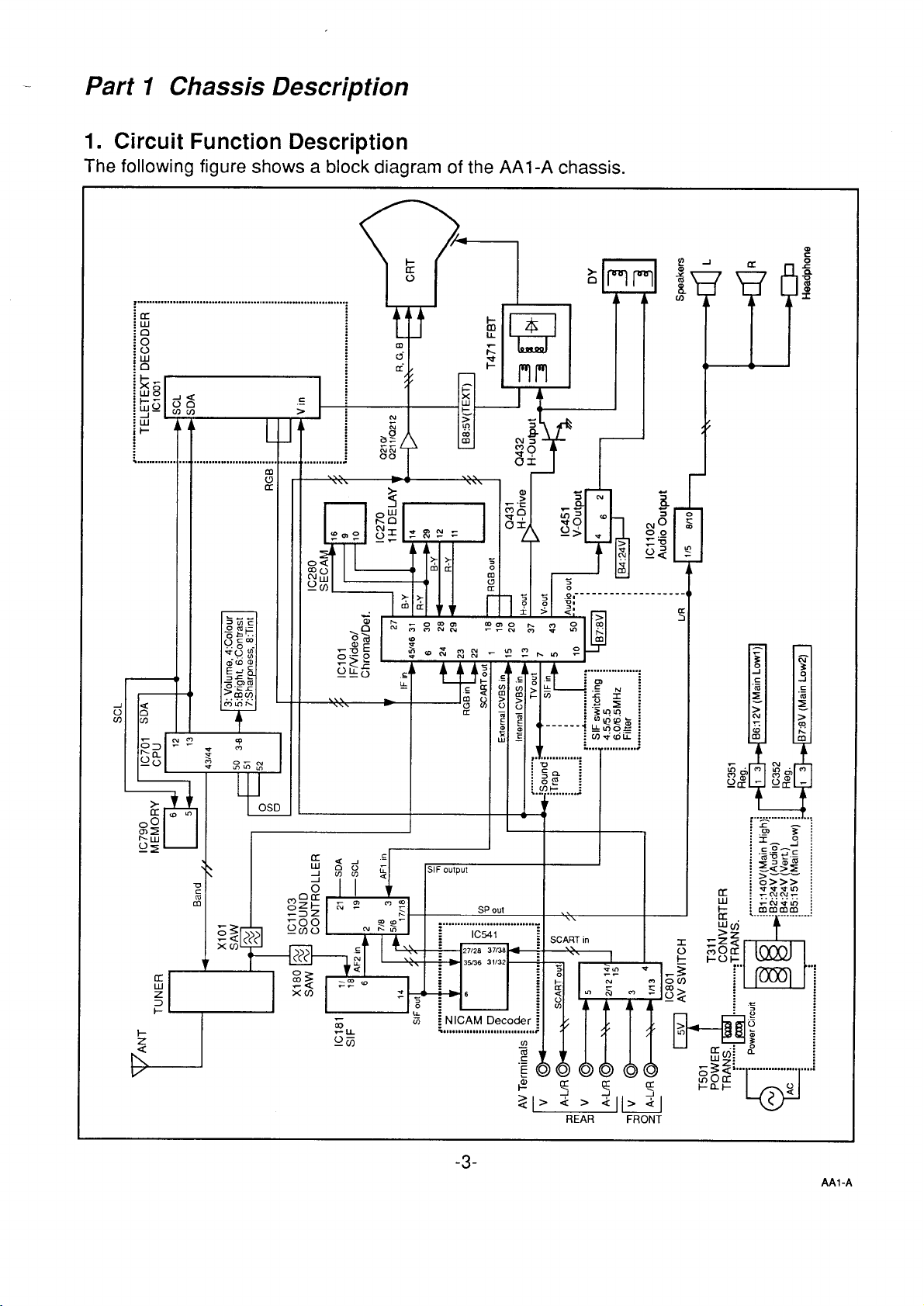
Part 1 Chassis Description
1. Circuit Function Description
The following figure shows a block diagram of the AA1-A chassis.
1
%
REAR
FRONT
-3-
AA1-A
Page 4
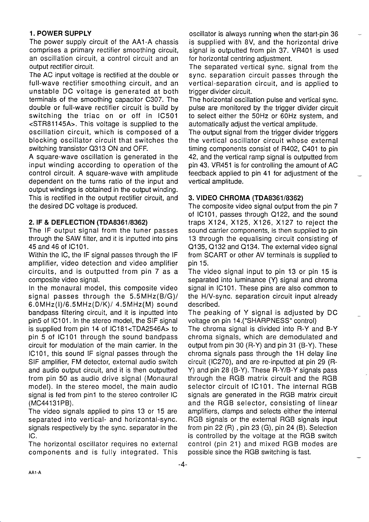
1. POWER SUPPLY
The power supply circuit of the AAl -A chassis
comprises a primary rectifier smoothing circuit,
an oscillation circuit, a control circuit and an
output rectifier circuit.
The AC input voltage is rectified at the double or
full-wave rectifier smoothing circuit, and an
unstable DC voltage is generated at both
terminals of the smoothing capacitor C307. The
double or full-wave rectifier circuit is build by
switching the triac on or off in IC501
<STR81145A>. This voltage is supplied to the
oscillation circuit, which is composed of a
blocking oscillator circuit that switches the
switching transistor Q313 ON and OFF.
A square-wave oscillation is generated in the
input winding according to operation of the
control circuit. A square-wave with amplitude
dependent on the turns ratio of the input and
output windings is obtained in the output winding.
This is rectified in the output rectifier circuit, and
the desired DC voltage is produced.
2. IF& DEFLECTION (TDA8361/8362)
The IF output signal from the tuner passes
through the SAW filter, and it is inputted into pins
45 and 46 of IC101.
Within the IC, the IF signal passes through the IF
amplifier, video detection and video amplifier
circuits, and is outputted from pin 7 as a
composite video signal.
In the monaural model, this composite video
signal passes through the 5.5 MHz(B/G)/
6. 0MHz(l)/6.5MHz( D/K)/ 4.5 MHz(M) sound
bandpass filtering circuit, and it is inputted into
pin5 of IC101. In the stereo model, the SIF signal
is supplied from pin 14 of IC181 <TDA2546A> to
pin 5 of IC101 through the sound bandpass
circuit for modulation of the main carrier. In the
IC101, this sound IF signal passes through the
SIF amplifier, FM detector, external audio switch
and audio output circuit, and it is then outputted
from pin 50 as audio drive signal (Monaural
model). In the stereo model, the main audio
signal is fed from pinl to the stereo controller IC
(MC44131PB).
The video signals applied to pins 13 or 15 are
separated into vertical- and horizontal-sync.
signals respectively by the sync. separator in the
Ic.
The horizontal oscillator requires no external
components and is fully integrated. This
AA1-A
oscillator is always running when the start-pin 36 –
is supplied with 8V, and the horizontal drive
signal is outputted from pin 37. VR401 is used
for horizontal centring adjustment.
The separated vertical sync. signal from the
sync. separation circuit passes through the
vertical-separation circuit, and is applied to
trigger divider circuit.
The horizontal oscillation pulse and vertical sync.
pulse are monitored by the trigger divider circuit
to select either the 50Hz or 60Hz system, and
automatically adjust the vertical amplitude.
The output signal from the trigger divider triggers
the vertical oscillator circuit whose external
timing components consist of R402, C401 to pin
42, and the vertical ramp signal is outputted from
pin 43. VR451 is for controlling the amount of AC
feedback applied to pin 41 for adjustment of the _
vertical amplitude.
3. VIDEO CHROMA (TDA8361/8362)
The composite video signal output from the pin 7
of IC101, passes through Q122, and the sound
traps X124, X125, X126, X127 to reject the
sound carrier components, is then supplied to pin
13 through the equalizing circuit consisting of
Q135, Q132 and Q134. The external video signal
from SCART or other AV terminals is supplied to
pin 15.
The video signal input to pin 13 or pin 15 is
separated into luminance (Y) signal and chroma
signal in IC101. These pins are also common to
the H/V-sync. separation circuit input already
described.
The peaking of Y signal is adjusted by DC _
voltage on pin 14.(’’SHARPNESS” control)
The chroma signal is divided into R-Y and B-Y
chroma signals, which are demodulated and
output from pin 30 (R-Y) and pin 31 (B-Y). These
chroma signals pass through the 1H delay line
circuit (IC270), and are re-inputted at pin 29 (R-
Y) and pin 28 (B-Y). These R-Y/B-Y signals pass
through the RGB matrix circuit and the RGB
selector circuit of IC101. The internal RGB
signals are generated in the RGB matrix circuit
and the RGB selector, consisting of linear
amplifiers, clamps and selects either the internal
RGB signals or the external RGB signals input
from pin 22 (R) , pin 23 (G), pin 24 (B). Selection
is controlled by the voltage at the RGB switch
control (pin 21) and mixed RGB modes are
possible since the RGB switching is fast.
-4-
—
Page 5

The RGB switch also functions as a fast blanking
pin by blanking the RGB output stages; here
internal and external RGB signals are overruled.
The RGB signals for the on-screen display are
superimposed onto the selected RGB signals at
the base of transistors Q21O, Q211 and Q212
respectively.
The saturation of colour gain is controlled by the
DC voltage of pin 26. (“COLOUR” control)
The contrast control voltage present at pin 25,
controls the RGB signal gain, and the brightness
control voltage present at pin 17, controls DC
level of RGB signals.
The RGB signals are finally buffered before
being presented to the RGB output pins [pin 20
(R), pin 19 (G), pin 18 (B)].
4. AUDIO OUTPUT
4-1 (AN5265)-Monaural model
The audio signal output from pin 50 of IC101 is
inputted to pin 2 of ICI 71 and passes through
the pre-amplifier circuit and the drive circuit into
the audio amplifier. The audio amplifier is the
SEPP (Single-Ended Push Pull) type and the
output from pin 8 drives the speaker directly.
4-2 (TDA7263M)-Stereo model
The audio signals output from pins 17 and 18 of
IC1l 01 (MC44131 PB) are inputted to pins 1(Left)
and 5( Right) of IC1102 and passes through the
pre-amplifier circuit and drive circuit, after which
it is input to the audio amplifier. The audio
amplifier is the SEPP (single-ended, push-pull)
OTL type and the outputs from pins 8( Right) and
10(Left) drive the speakers directly.
5. VERTICAL OUTPUT
An LA7833 is used for the vertical output circuit
in this chassis. The vertical ramp signal from pin
43 of IC101 is inputted to pin 4 of IC451. This
ramp drives IC451, and vertical scanning is
performed. In the first half of scanning a
deflecting current is outputted from pin 2 and
passes through the following path:
VCC(B4)+D451+ pin 3+ pin 2+ DY+ C461+
vR451/R459.
An electric charge is then stored in C461. [n the
last half of scanning the current path is:
C461+ DY+ pin 2+ pin 1+ VR451/R459 +
C461
In this way, an increasing
current flows directly to
sawtooth waveform
the DY to perform
electron beam deflection. During the first half of
the blanking period the vertical ramp signal
suddenly turns OFF. Since there is no longer any
current flowing into the DY, the magnetic field
collapses causing an induced current to flow as
follows:
pin 2+ pin 1+ VR451/R459+ C461 + DY
DY+
Once the magnetic field in DY has dissipated,
the current path becomes:
Vcc+ pin 6+ pin 7+ C452+ pin 3+ pin 2 +
DY+ C461 + VR451/R459
and when the prescribed current value is
reached, the vertical drive ramp signal turns ON.
This completes one cycle.
6. HORIZONTAL OUTPUT
The horizontal oscillation signal is outputted from
pin 37 of IC101 and used to switch the drive
transistor Q431. This switching signal is current
amplified by the drive transformer T431 and
drives the output transistor Q432. When Q432
turns ON, an increasing current flows directly to
the DY through
C441/C442+ L441/R441 + DY+ Q432-C +
Q432-E
and the deflection occurs during the last half of
the scanning period. When Q432 turns OFF, the
magnetic field stored in the DY up to that point
causes a resonant current to flow into the
capacitors C420 and C423 and charges them.
The current stored in C420 and C423 then flows
back to the DY causing an opposite magnetic
field to be stored in the DY. This field then
collapses increasing a current which switches
the dumper diode in Q432 ON. The resonance
state is completed, and an increasing current
then flows again directly to the DY through the
dumper diode.
By this means, the deflection in the first half of
the scanning period is performed. When Q432
turns ON at the end of the first half of the
scanning period, the deflection during the last
half is begun, thus completing one cycle.
In the PCC circuit consisting of Q461 and Q462,
the parabola signal supplied from the vertical
circuit is added at the horizontal output stage and
pincushion compensation is performed by
varying the DC bias. Further, the ABL voltage is
fedback to the base of Q462 to compensate for
width variations due to variations in the beam
current.
-5-
AAI-A
Page 6
2. CPU
The following figure shows a block diagram of the CPU peripheral circuit.
il
!
I
I
0 a
cu.
—.—. —
—-—. — .
AA1-A
!7-—. —-— -’
-6-
a
c
u
Page 7

The following table shows pin descriptions of the CPU.
Pin Description
1 Horizontal sync. signal input
2 Vertical sync. signal input
3 Volume control output
4
Colour control output
Brightness control output
5
6 Contrast control output
7 Sharpness control output
8 Tnt control output
9 AV1/AV2 switch output (AV1 :Low)
10 TV/AV switch output (TV: Hi)
11 AFT S-signal input
12
13
ipc bus SCL line
12C bus S(JA line
14 Tuning voltage output
15 Ident signal input
16
RC signal input
17 --18
19
20
Chroma ID input
Ignore signal input
Sync. ID input
21 ---
22
23
24
25
26
GND
GND
Oscillator input for CPU
Oscillator output for CPU
GND
Pin Description
27 +5V
28
29
30
31
power supply
Oscillator 2 for OSD
Oscillator 1 for OSD
Reset input
Detection power failure (Error: Lo)
32 AV2 option switch (Hi: AV2)
33 Option switch (System selection)
34 Key scan input (DV)
35
Key scan input (DC)
36 Option input & SIF output D/K
37 Option input & SIF output I
38 Option input & SIF output B/G
39 Option input & SIF output M/M
40
41
42
System switch output SECAM
System switch output 3.58
System switch output 4.43
43 Band switch output I (Low: VH)
44
Band switch output II (Low: VL)
45 AC switch off detection input
46
47
Option switch (RC status)
Sound mute output (Mute on:Low)
48 Power on/off output (P-On: Hi)
49
Blanking signal output for OSD
50 OSD blue signal output
51 OSD green signal output
52 OSD red signal output
-7-
AAI-A
Page 8
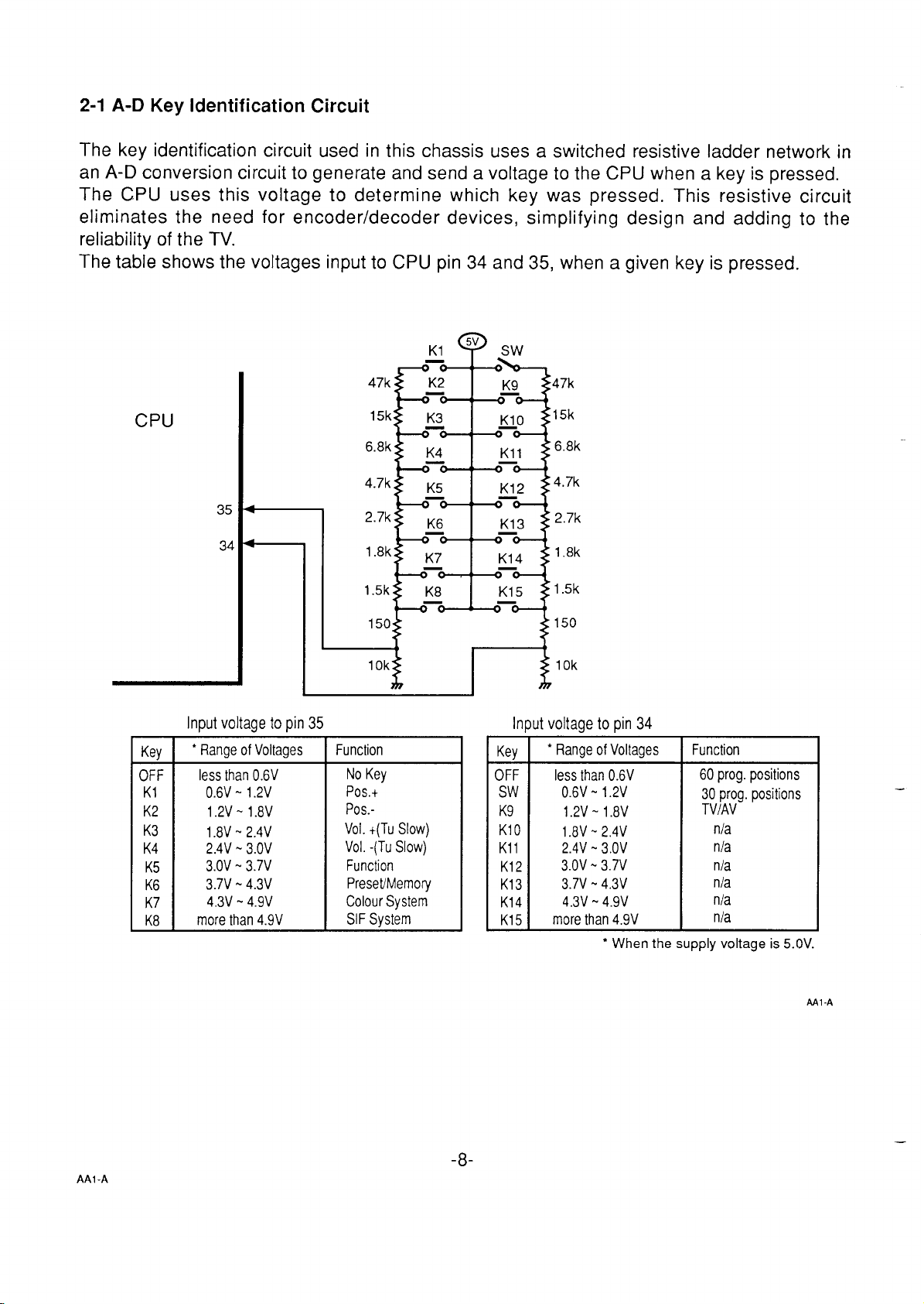
2-1 A-D Key Identification Circuit
The key identification circuit used in this chassis uses a switched resistive ladder network in
A-D conversion circuit to generate and send a voltage to the CPU when a key is pressed.
an
The
CPU uses this voltage to determine which key was pressed. This resistive circuit
eliminates the need for encoder/decoder devices, simplifying design and adding to the
reliability of the TV.
The table shows the voltages input to CPU pin 34 and 35,
K1 5“ SW
Q
when a given key is pressed.
47kzizEa47k
CPU
4
35
34 +
Inputvoltageto pin 35
I Kev I ● flangeofvolta9es I Function
OFF
K1
K2
K3
K4
K5
K6
K7
KR
lessthan0.6V
0.6V- 1.2V
1.2V- 1.8V
1.8V- 2.4V
2.4V- 3.OV
3.OV- 3.7V
3.7V- 4.3V
4.3V- 4.9V
morethan4.9V
15’ K3
6.8k K’
4.7’ K5
2.7’ K6
1.8’ ~7
1.5’ K8
NoKey
Pos.+
Pos.vol.+(TuSlow)
Vol.
-(Tu Slow)
Function
PreseUMemory
ColourSystem
SIFSvstem
&o
— —
—
— —
— —
— —
[:1
Kll
~2
K13
K14
K15
15’
6.8’
4.7’
2.7’
1.8’
1.5’
150
$
10k
i
Inputvoltageto pin34
Key
OFF
Sw
K9
K1O
Kll
K12
K13
K14
K15
-,
● RangeofVoltages
lessthan 0.6V
0.6V- 1.2V
1.2V- 1.8V
1.8V-J2.4V
2.4V--3.OV
3.OV- 3.7V
3.7V- 4.3V
4.3V- 4.9V
morethan4.9V
● When the supply voltage is 5.oV.
Function
60prog. positions
30prog. positions
TVIAV
n/a
nla
nla
nla
nla
nla
AA1-A
AA1-A
-8-
Page 9

2-2 Option switches
This chassis uses the option function switches to determine several different specifications of
TV set.
the
The CPU determines the specification of TV by detecting the voltage level on the following
pins.
Colour system: pin 33, SIF system: pins 36 to 39, No. of AV modes: pin 32, Remote control
status: pin 46, No. of programme position: pin 34.
Pins 36 to 39 also operate as SIF system selection outputs.
Colour system
system
SIF
CPU
--13
Pinll
Ov
0.5V
1.2V
1.8V
2.5V
3.OV
3.8V
4.3V
4.9V
r
Rx
open
82k
33k
18k
10k
6.8k
3.3k
1.5k
150
CPU
5
Rx
33
10k
Specification
Test
PALsystem
VMT system(PAL-TV, PAL/M-NTST/NTSC-AV)
East Europe system(PAL/N-NTSC/S ECAM-TV,AV)
Multi system(PAUM-NTSC/NTSC/SECAM-TV,AV)
China system(PAUM-NTSC/NTSC-TV,AV)
nla
nla
nla
10kx4
Swl
on
on
off
off
on
off
r
SW2 SW3 SW4
on
off on off
off
off on off
off off off
off off off
IL
39
38
37
36
on on
on
on
-9-
Specification
No SIF system
SIF system e (B/G, D/K)
SIF system d (M/M, B/G)
SIF system c (M/M, B/G, D/K)
SIF system b (B/G, 1,D/K)
SIF system a (B/G, D/K, 1,M/M)
AAl-A
Page 10

AV modes
CPU
32 -
Remote control status
CPU
46
10k
“9
5
10k
9
P-
SW5 Specification
2 AV system (AV1/AV2)
11 AV system (AV)
Specification
w/o remote control function
w/ remote control function
I
off
on
SW6
off
on
I
No. of programme position
CPU
34
H
5
7’
d
Sw
Rx=
47k+15k+6.8k+4.7k
+2.7k+l .8k+l .5k+150
10k
Sw
off
on
Specification
60 programme positions
30 programme positions
AAl A
AA1-A
-10-
Page 11

2-3 System switch output
The outputs from pins 40 to 42 of the CPU select the colour system and the outputs from
36 to 39 the
SIF system. These outputs drive the colour and SIF system switching circuits.
pins
The operation of each switching circuit is shown in the tables below.
.
Colour system sw
v
SECAM
I
I NTSC
SIF system switching output
1. Multi system(SIF system a option)
SIF system
thing output
Output pins
42 41 40
HHL
HLL
HLH
LHL
Output pins
Display
Auto
PAL/NTsc4.43
SECAM
NTSC
Display
39 38 37 36
Auto
B/G-5.5MHz
I-6.OMHZ
D/K-6.5MHz
M/M-4.5MHz
●
LHLL
LLHL
LLLH
HLLL
HHH
● It depends on receiving TV system
S1
S2
S3
S4
S5
2.3 system (SIF system b option)
~
B/G-5.5MHz
I-6.OMHZ
D/K-6.5MHz
3. China, PX (SIF system c option)
SIF system
input H
I
input L
input L
Output pins
39 38 37 36
●
Auto
H
BIH-5.5MHZ LH
DIK-6.5MHz LL
MIM-4.5MHZ HL
Display
S1
LL
HL
LH
input H
input L
input H
input L
● Itdepends on receiving TV system
S2
S3
S4
Display
S1
S2
S3
S4
-11-
AA1-A
Page 12
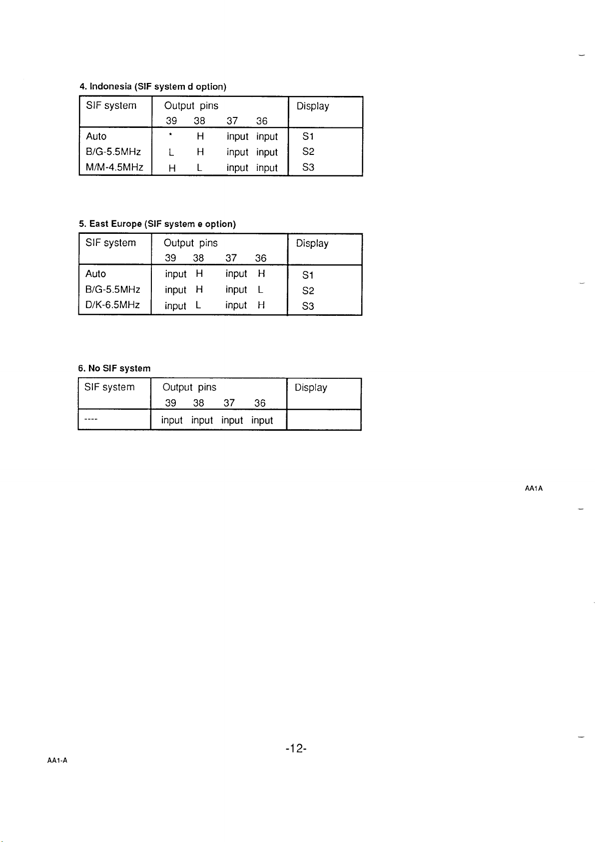
4. Indonesia (SIF system d option)
SIF system Output pins Display
39 38 37 36
●
Auto
BIG-5.5MHZ
MIM-4.5MHZ
5. East Europe (SIF system e option)
H input input S1
LH
HL
input input S2
input input
S3
SIF system
Auto
B/G-5.5MHz
D/K-6.5MHz
6. No SIF system
SIF system Output pins
----
Output pins
I
39 38 37 36
I
input H
input H
input L
39 38 37 36
input input input input
input H
input L
input H
Display
I
I
Display
S1
S2
S3
AAlA
—
AA1-A
-12-
Page 13
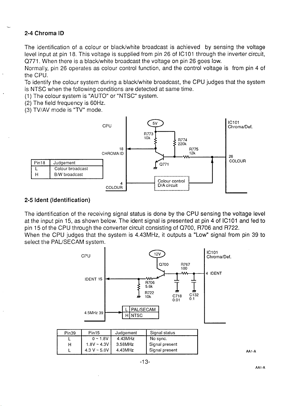
2-4 Chroma ID
The identification of a colour or black/white broadcast is achieved by sensing the voltage
level input at pin 18. This voltage is supplied from pin 26
Q771. When there is a black/white broadcast the voltage on pin 26 goes low.
Normally, pin 26 operates
as colour control function, and the control voltage is from pin 4 of
of ICI 01 through the inverter circuit,
the CPU.
To
identify the colour system during a black/white broadcast, the CPU judges that the system
is NTSC when the following conditions are detected at same time.
(1) The colour system is “AUTO” or “NTSC” system.
(2) The field frequency is 60 Hz.
(3) TV/AV mode is “TV” mode.
CPU
CHROMA ID
btE!zzd
COLOUR
18
R773
10k
4
....................................
4
i Colour control
~ D/A circuit ~
....................................
R774
220k
1 “T
R775
12k
U
ICI 01
Chroma/Def.
26
COLOUR
2-5 Ident (Identification)
The identification of the receiving signal status is done by the CPU sensing the voltage level
at the input pin 15, as shown below. The ident signal is presented at pin 4 of IC101 and fed to
pin 15 of the CPU through the converter circuit consisting of Q700, R706 and R722.
When the CPU judges that the system is 4.43MHz, it outputs a “Low” signal from pin 39 to
select the PAUSECAM system.
CPU
0
12V
ICI 01
I
Chroma/Def.
Pin39
L
H
L
IDENT 15
4.5 MHZ 39
Pin15
O-1.8V 4.43 MHZ No sync.
1.8V - 4.3V
4.3 v -
5.OV 4.43 MHZ Signal present
Judgement
3.58 MHz Signal present
-13-
,
Signal status
AA1-A
AAl -A
Page 14
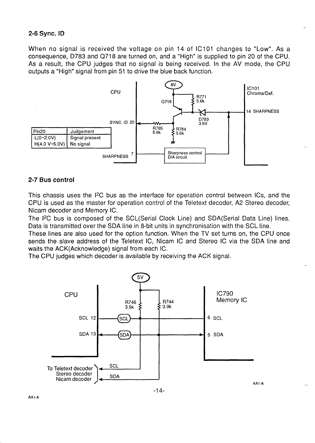
2-6 Sync. ID
When no signal is received the voltage on pin 14 of IC101 changes to “Low”. As a
consequence, D783 and Q718 are turned on, and a “High” is supplied to pin 20 of the CPU.
As a result, the CPU judges that no signal is being received. In the AV mode, the CPU
outputs a “High” signal from pin 51 to drive the blue back function.
—
CPU
Q718
a
SYNC. ID 20
R785
5.6k
E!zE5E9
SHARPNESS 7
2-7 Bus control
This chassis uses the IPC bus as the interface for operation control between ICS, and the
CPU is used as the master for operation control of the Teletext decoder, A2 Stereo decoder,
Nicam decoder and Memory IC.
The IPC bus is composed of the SCL(Serial Clock Line) and SDA(Serial Data Line) lines.
Data is transmitted over the SDA line in 8-bit units in synchronisation with the SCL line.
These lines are also used for the option function. When the TV set turns on, the CPU once
sends the slave address of the Teletext IC, Nicam IC and Stereo IC via the SDA line and
waits the ACK(Acknowledge) signal from each IC.
The CPU judges which decoder is available by receiving the ACK signal.
—;
.......................................
Sharpness control
~ D/Acircuit
.......................................
:4
Iclol
Chroma/Def.
14 SHARPNESS
L
AA1-A
CPU
SCL 12
SDA 13
IC790
R746
3.9k
d
Memory IC
6 SCL
5 SDA
AAl -A
.
Page 15

2-8 Band switching circuit
The band switching control signals are outputted from pins 43and440f the CPUand fed to
the base of Q781, Q782 and Q784, band switching transistors.
The one of these transistors then outputs the drive voltage(+l 2V) to the tuner according to
output signal as shown below table.
When the UHF band is selected, “High” signal are sent from both pins 43 and 44. The D781
and D782 are cut off, then Q784 and Q783 are turned on and +12V is supplied to UHF
terminal on the tuner.
Antenna
Tuner
4
L
VI-
VH
s-
Q781
0782
44 BandII
4.7k
43 Band I
4,7k
CPU
4
u
Band Switching Logic
output
Pin43 Pin44
H
L
H H
Q783
L
H
Q784
* ---
1
Q781 Q782 Q783
I
on
off
off
off off
on off VHF-High
off on UHF
Selected Band
I
VHF-Low
-15-
AAl -A
AA1-A
Page 16
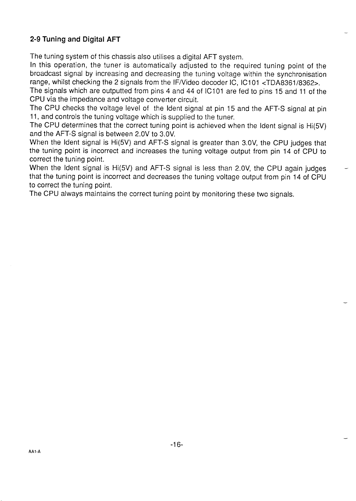
2-9 Tuning and Digital AFT
The tuning system of this chassis also utilises a digital AFT system.
In this operation, the tuner is automatically adjusted to the required tuning point of the
broadcast signal by increasing and decreasing the tuning voltage within the synchronisation
range, whilst checking the 2 signals from the lF/Video decoder IC,
The signals which are outputted from
pins 4 and 44 of IC101 are fed to pins 15 and 11 of the
ICI 01 <TDA8361/8362>.
CPU via the impedance and voltage converler circuit.
The CPU checks the voltage level of the Ident signal at
11, and controls the tuning voltage which is supplied to the tuner.
pin 15 and the AFT-S signal at pin
The CPU determines that the correct tuning point is achieved when the Ident signal is Hi(5V)
and the AFT-S signal is between 2.OV to 3.OV.
When the Ident signal is Hi(5V) and AFT-S signal is greater than 3.OV, the CPU judges that
the tuning point is incorrect and increases the tuning voltage output from pin 14 of CPU to
correct the tuning point.
When the Ident signal is Hi(5V) and AFT-S signal is less than 2.OV, the CPU
that the tuning point is incorrect and decreases the tuning voltage output from
again judges –
pin 14 of CPU
to correct the tuning point.
The CPU
always maintains the correct tuning point by monitoring these two signals.
AA1-A
-16-
Page 17

Tuner
TU
/
Q711
\
CPU
14
TUNING OUT
IDENT IN
AFTIN 11
15
4
I
z
C746 R722
0.01 10k
4
R780
150k
R706
5.6k
(k
Q700
\
R767
100
w
; ;;:’ ; :.;32
R121
68k
w
I
z :.;:$
R123
“Ok
Iclol
lF&VIDEO
, 4 IDENT(T.B.)
44 AFT
Input Signal
Pin 11
of IC701
Pin 14
of IC701
Pin 15
of IC701
AFT S-Curve
Input
Tuning Voltage
Ident
Signal Input
/
,
,:, ,,),
,!. .,.
I Imut Voltacie Level of Pin 11 I
LL(oV-1 .5V)
L (1.5V-2.OV)
M (2.O-2.5V)
H (2.5V-3.OV)
HH(3.5V-5V)
\
,,, ,
3.5V
3.OV
2.OV
1.5V
Ov
‘ Tuned point
Judgement
Tuning Voltage Down
Tuning Voltage Down
Tuned
Tuning Voltage Up
Tunina Voltaue Up
-17-
AA1-A
Page 18

2-10 Power On/stand-by and Protection circuit
~lj
Power On/Stand-by
The power on/stand-by signal is outputted from pin 48 of CPU.
When the stand-by mode is selected the voltage of pin 48 changes from Hi(5V) to
Low(OV), which turns Q792 off and Q793 on. Q793 drives the photo-coupler D315 which in
turn drives Q312 on. Finally Q312 stops the oscillation of power circuit switching the TV
into the stand-by condition.
At the same time, Q793 drives the LED, D1120 to illuminate and indicate the stand-by
mode.
Protection circuit
A protection circuit is provided to protect the TV set in case of a circuit malfunction.
When an abnormality occurs during TV reception it causes pin 31 of the CPU to go
continually Low (less than 2.OV). After one second, the CPU detects that a power failure
has occurred on the TV set, and the CPU turns the TV into the stand-by condition.
CPU
POWER 48
PROTECT
31
IN
. . . ... . ... . . .. .
.
.
.
.
,
.
\5viZiiZ’iJStand-By ,V
5V
9
11‘“fF%@ ‘i
,....................
7
..:
D362
I I
D363 10V
..-
\
/
... —-. —,
Power
Oscillation
Circuit
I
Q312
—.. — ..j_
—.. —..
..................................
.................................,
.................................
1
AAI -A
K\) —
f
.J.
Jormal
operation ........................ ... ... ... ..Ov
-“”””””’~m~ii6 ~-= ~:!~~:rmer~
Power failure ‘“” """"""""""""""c`J""""""""""""""""""'""""--"""""""""""-
i
...
D468
~
&!
-18-
................................
-.. —.. —..l —
MI-A
1<
:LL
—-
Page 19

2-11 Horiz./Vert. pulse input
The vertical and horizontal pulse from the deflection circuits are inputted to pins 1 and 2 in
order to synchronise the On Screen Display.
The vertical pulse inputted to pin 2 is made by the sandcastle pulse which is outputted from
pin
38 of ICI 01. The sandcastle pulse is extracted the horizontal components at the CR
integrating circuit consisting of R796 and C791.
The horizontal pulse inputted to pin 1 is made by the retrace pulse which is generated on pin
5 of flyback transformer.
If one of these pulses is not supplied to the CPU, the on-screen display cannot be displayed.
CPU
H-SYNC. 1
V-SYNC. 2
-1u’1 EY
Horiz.
I
IL---A
Hor]z,
\
4111111111111111111111111
Iclol
lF/Video/Chroma
w
38
J
Veri.
-19-
AA1-A
AAI-A
Page 20

3.System switches
The following diagram shows the multi system, selection circuit of this chassis.
The description on the following page, describe these switches which are controlled by IC701
(CPU) output.
101 (TDA8362
13 :
F in
V ir
1“””’””””””””-””--/S2
TV 011[
R=
NTSC
Band Limitter
SECAM
REF.
5
●
in
;IF
CHROMA IE
IDENT
(Time Base
NH
$3 W8
j
u3-
.... ... .. ...... .. . ... .. ..
f’ {
HUE
. . . . ;
+
(Q203) ;
>’
z+
.............................................. ......................
IC701(CPU) :
lE
-’o”’
1:
IDENT 4.5 3g------.--.o;5:.-
..
42
$.43
41
.......
3.58
50/60 ID ,:/
2
....................................................
........
..................
5.5 .38..-.-.--.-----; 1
Go 37 ;
65 36. ; ~
:::
:~
:!
:!
::
:::
:::
;;:
,,:
IC280
(SECAM)
::
I
:
.....
_ V-SYNC. Pulse
(for OSD)
AA1-A
SIF Filter
6.OMHZ Filter
5.5 MHz Filter
4,5 MHz Filter
+5-%
S9
(Q155)
J-c%
S8
(Q154)
+h-
S7
(Q152)
........................................................
.
AAl-A
-20-
Page 21

The system switches (S1 -S1O) are used for multi-standard model.
(Refer to the block diagram of system switching circuit on previous page)
SI :
Switch for band-limiting on NTSC(3.58) mode (Dl 06)
This switch is driven by ON/OFF signal from CPU (pin39).
S2:
Switch for sound carrier trap on NTSC(3.58) mode (Dl 20)
This switch is driven by signal from CPU (pin39).
Switch for sound carrier trap except NTSC(3.58) mode (DI 21)
S3:
This switch is driven by inverting signal from CPU (pin39).
System switch for forced SECAM mode (Q203)
S4 :
This switch is driven by ON/OFF signal from CPU (pin40).
System switch for forced 4.43 mode (Q222)
S5 :
This switch is driven by ON/OFF signal from CPU (pin43).
Note: When the colour system is set to “AUTO”, both S6 and S7 will turn on.
System switch for forced 3.58 mode (Q221 )
S6:
This switch is driven by ON/OFF signal from CPU (pin42).
System switch for 4.5 MHz filtering on NTSC(3.58) mode (Ql 52)
S7:
This switch is driven by ON/OFF signal from CPU (pin39).
System switch for 5.5 MHz filtering on B/G mode (Ql 54)
S8:
This switch is driven by ON/OFF signal from CPU (pin38).
System switch for 6.OMHZ filtering on I mode (Ql 55)
S9:
This switch is driven by ON/OFF signal from CPU (pin37).
S1O: System switch for 6.5 MHz filtering on D/K mode (QI 56)
This switch is driven by ON/OFF signal from CPU (pin36).
Note: When the TV system is set to “AUTO”, S7, S8, S9 and S1 O will turn on.
-21-
AA1-A
Page 22

3-1 Sound Carrier Trap Circuit
When the 4.5 MHz system is selected, the CPU outputs a “High” signal from pin 39. Q153 is
turned on and Q157 is turned off. As a result D121/Dl 23 are cut off and D120 is turned on.
The composite video signal from pin 7 of IC101 is supplied to the base of Q135 via the
4.5 MHz trap circuit Xl 25 which removes the intercarrier sound content. From the equalizing
circuit the CVBS video signal is fed to pin 13 of IC101. When other systems are selected the
composite video signal is fed through the 5.5 MHz/6 .0MHz trap X126, or the 6.5 MHz trap
Xl 27, which remove the respective intercarrier sound contents. The remaining video is fed to
pin 13 of IC101 via the video equalizing circuit to compensate the characteristic of video .
This switching is shown in the table be~ow.
CVBS in 13
Iclol
lF/Video/chroma
CVBS out 7
CPU
4.5 MHZ 39
d
II
C216
0.1 I: :$;;,
—.—-
. .
,*,
R134
lk
-. —- —_ — _________________ :
L124
X124
5.5 MHz
—.m .->’
X125
X126
‘
5.516.OMHZ
X127
6.5 MHz
R156
33k
R137
220
– —- —DJ=-— 150
1’
Q122
I
R158
1.8k
R195
27k
D121
R149
680
R138
4“Jp
~w K ‘
R139
~126 4.5 MHZ
100
R148
‘w
680
w
D123
I: Video
~ ~ Equalizing
i ~ g;;;j
R14 :.......
27k
‘1
...........................
AA1-A
SIF System
4.5 MHZ H On off
Other
I
Pin 39
L
II
Q153
off
Q157
I
-22-
On
D120
On off
on On
D121
Page 23

3-2 SIF Filtering Circuit
In the stereo model, the SIF signal is outputted from pin 14 of IC181 and is supplied to the
base of the buffer transistor Q1 82.
In the monaural model, the video signal which also contains the SIF carrier signal is outputted
from pin 7 of IC101 and is supplied to the Qlll.
The SIF signal output from Q181 is supplied to pin 5 of IC101 through the sound bandpass
filtering circuit. The relevant bandpass filters Xl 51 (4.5 MHz), Xl 52 (5.5 MHz), Xl 53 (6.OMHZ),
Xl 54 (6.5MHz) are selected according to the output signals from pins 36 to 39 of the CPU.
The SIF signal is then fed via the relevant buffer Q152 (4.5 MHz), Q154 (5.5 MHz), Q155
(6.OMHZ), Q156 (6.5MHz) to the SIF input pin 5 of IC101 for de-modulation.
CVBS Output
SIF Input 5
Iclol
If/Video
/chroma
4.5 MHZ 39
CPU
5.5 MHZ 3[
.........................................................................................................................................................,
7
Sound Carrier
4
CVBS+Sound Carrier Outwt i
....................................................................................................
SIF Filterina Circuit
ni~?
X151
4.5 MHZ
+111-www-f
E-w
0112
C141
F
I
Q153 0157
Q154 -
I
IC181
SIF decoder
14
.............. ,_
Q182
(Qlll) c
‘4
R184
:Rlll)
3
8
.—
2
k
k
6.OMHZ 37
6.5 MHz 36
~
i
Q-f
SIF System Pin39
Auto
5.5 MHZ
6.OMHZ L
6.5 MHz L
4.5 MHZ
T
●
L
H
Pin38
H
H
L
L
L
II
X154
6.5 MHz
Pin 37 Pin36
H H
L L
H L
L H
L L
T
-23-
F-J
Q152 Q154 Q155 Q156
*
On On On
off On off off
off
off off off On
On off off off
off On off
‘ Itdependson receiving system,
AA1-A
Page 24

3-3 Chroma Crystal Selection
The subcarrier oscillator crystals, X201 for 4.43 MHz and X202 for 3.58 MHz are used for both
colour demodulation and sync. calibration circuits in IC101 (TDA8362).
When the colour system is AUTO, the output signals from pins 42 and 41 of IC701, CPU, are
“High”, causing Q221 and Q222 to be turned off, and both X201 and X202 are available for
oscillation.
IC101 identifies the colour subcarrier of the incoming signal and selects the
correct crystal oscillator.
When the forced NTSC system is selected, the CPU outputs a “High” from pin 41 and a
“Low” from pin 42. Q221 is turned on and Q222 is turned off. As a result, the oscillation of
X201 for 4.43 MHz is stopped by applying the DC voltage.
For other colour systems using 4.43 MHz oscillation in a forced mode, the CPU outputs a
“High” from pin 42 and a “Low” from pin 41 which turns Q221 off and Q222 on. The result is
that X202 is prevented from oscillating by the application of the DC voltage via Q222.
Crystal Select
—
CPU
3.58MI+z 41
4.43 MHz 42
System
Auto
PAUNTSC4.43
SECAM
NTSC
R228
4.7k
Vvv
R224
15k
I
4.7k
1,= ,,,_’- ,
.Vv
R222
4.7k
\
R229
4 JI
1
Q222
.......... . . . . . . . . . . . . . .... ..
Q221
R223
47k
Vvv
47k
Vvv
I-$ N-EC
Pin 41 Pin42 Q221 C1222
H H
L
L H
H L
H
off off
off On
off On
On off
1
X202
? 3“58MH’i 1
1X201
~4.43MH;
L
c,20f3
J-
X201
Live
Live
Live
Dead
Iclol
Video/chroma
34 3.58 MHz
...>
35 4.43 MHZ
X202
Live
Dead
Dead
Live
AA1-A
AAI-A
-24-
Page 25

4. Internal/External source selection
This circuit is for the selection of external AV input source or internal source. The external AV
source (AV1 and AV2) are applied to the AV switching IC, IC801. When the AV1 mode is
selected, the AV1/AV2 switching signal from pin 9 of the CPU outputs “Low” to pins 9, 10 and
11 to select the AV1 source, and then the video, audio-L and audio-R signals are sent from
pins
4, 15 and 14 to the next stage respectively.
the video signal, the selected external video signal is supplied to pin 15 of IC101 and the
In
internal video signal supplied to pin 13. The selection of internal or external video source is
performed in the IC101 by the TV/AV drive signal sending from pin 10 of the CPU via inverter
transistor Q202.
In the audio signal, the selected audio signals(L/R) are supplied to the sound control IC,
IC1l 02, MC44131 PB, and the selection of external or internal audio source is performed by
the bus lines.
The following tables show the TV/AV and AV1/AV2 switching logic output from the CPU.
0 ~;; VIDEO IN
O AV1 AUDIO L.IN
0 AV2
Iclol
J
–13
Iternal Video Input
k
)
–15
;xternal Video Inpu
-..16
Q202
IC801
AVIIAV2 switch
1
3
4
...........
{:
;;
~:
;:
~;
..........................
.......
....................
~~~ ‘uD’OR-’N
\
Internal Audio L/R
16
External
Audio
L
15
14
R
11
10
9
AV1IAV2
TVIAV
4’”
g
*
5
bm
K&
H
SG
mm;
o=
~3~
@
A
Bus
/ ;
12113
9
SCIJ
SDA
10
4
SPEAKERS
CPU
AA1-A
-25-
AA1-A
Page 26

5. lF/Video/Chroma/Def. Circuit
The following figure shows a block diagram of the lF/Video/Chroma/Def IC peripheral
13
0
$1
n
s
mm ml
J.
y.”. ----
---
nnn
mu-)(i)
000
Zz iif
1
.
circuits.
i
3.
>-3
cd.
‘=*
A
A
4
1-
-26-
Page 27

6. Audio Circuit
The audio circuit of the AA1-A chassis has been designed for use the following circuits.
(1) Monaural circuit
(2) A2 stereo circuit
(3) A2 stereo and Nicam circuit
Monaural circuit
6-1
The
following figure shows a block diagram of the monaural audio peripheral circuits.
CPU
ICI 01<TDA8362>
lF/Video/Chroma
45
46
External Audio Input
6
CVBS
7
-
: SIF
Filtering ~
~
Circuit :-
IC801
.,,,,,,,,,,,.
~Avl A.di.
j
15:
,J #-@AV2 ‘“put
1............
/
;~6.5MHz from pin36 of CPU
4.5MHz frompin39of
5,5 MHz from pin38 of CPU
6.OMHz from pin37 of CPU
CPU
................”..............,,:
—
50
Audio signal
-S1F Carrier
5
4udio out
1
IC1102
Audio 0U@Jt<AN5265s
I
Q857K?858
Audio
output
~1 C“23
Mute
47
Speaker
3
Vol~me Control
Q705
{
Headphone
-27-
AA1 -A
Page 28

6-2 A2 stereo circuit
The following figure shows a block diagram of the A2 stereo audio peripheral circuits.
Nr.INN
1111
>>2>
m,lno$
=rLr3wul !--
I-!P
~
IL
I,,“ . . . . . . . . . . . . . . . . . . . . . .
“=
;
~
E‘z
u?
:_, _
mu
,9 y
:9
<=<<
52
)0
7
L
~3
+5Q’
26
-lU
......................................................................
?
:
~
m
‘Q
n
~
(m
al
a
:
An%
:
........;
co
E!i
I
0
u-l.’=
g
2
~
AA1-A
\
u
qns
I
Uy?w
,.,,................
/)
-28-
...” . . . . . . ...”....
1
0
(n
Page 29

6-3 A2 stereo and Nicam circuit
The following figure shows a block diagram of the A2 stereo and Nicam audio peripheral
circuits.
~msvvas
.. ..... .............. . ..”.”,O.,-,...”...-.”. ..”.!..
mu
L-
c?
A
................. .,I,.,,.,,.,.,.,.,
...............
.. ............... .....
... ..................
,.,.,
....
.
3
n
s
0
8
.=
c
I..........................,.,,.
u)
c
.—
&
E“%
u?
—.-
(00
........ ..........................
r
A
Z
5
,-
qns
u!ew
,.....,.,,..”...,..................................................
!
I
.
-29-
Page 30

7. Double/Full-wave rectifier circuit
The rectifier circuit of this chassis is employed the double/full-wave rectifier switching circuit
to operate the power supply circuit in stability from 90V to 290V AC input.
The fig. 1 shows the double/full-wave rectifier switching circuit using the triac IC STR81145A,
IC501 .
The triac in the IC501 automatically switches on or off to build up the double or full-wave
rectifier circuit according to the input AC voltage level.
In the range from 90V to 145V AC input, the double rectifier circuit is build up by switching the
triac on in the IC501 as shown in fig.2.
During the positive half cycle of AC input, the current flows as follows; AC(plus)+ IC501 pin2
+ pin3 + C509 + D509 + AC(minus). The voltage is charged in C509. During the
negative half cycle, the current flows as follows; AC(minus)+ D508 + C508 + IC501 pin3 +
pin2 + AC(plus). The voltage is charged in C508. As a result, the DC voltage which is
double of AC input voltage is observed between the output terminals KG-1 and KG-2.
In the range from 145V to 290V AC input, the full-wave rectifier circuit is build up by switching
the triac off as shown in fig.3.
During the positive half cycle, the current flows as follows; AC(plus) + D506 + C508/C509 +
D509 + AC(minus), and the negative half cycle, AC(minus) + D508 + C508/C509 + D507
+ AC(plUS). The voltage is charged in C508/C509. As a result, the DC voltage which is
same level of AC input voltage is observed between the output terminals KG-1 and KG-2.
This circuit can be supplied the proper DC voltage to the power oscillation circuit when the
AC input voltage varies in the range from 90V to 290V.
.............................
<
!Power ~
c307~Oscilation j
:Circuit :
:
AC Input
VAC
SW501
D506
R508A
~ KG-1 ,
Q
/u ~’
VDC
—
D501
R503
Vi= VAC’@ V~c= 2*Vi
@iz3–
+Fj;i
VACQ
<--------------------- -------------’ -
Fig.2 Double Rectifier& Smoothing Circuit
AAI -A
1)
L
L:504 C507
Vi
,:1
*vivw=zw
‘
C509
2
4
~ KG-1
J
KG-2
N
[5
-30-
~KG-2 :
3
IC501
STR81 145A
Main Unit
~
:,,,.,.,,,,,,,...,.,,,,,,,,,,,,,,,,,,,,,,,,,,0,,,,
Vi= VAC‘G VDC= Vi
--
— -- —-—-J IC501
I
Fig.3 Full Waveform Rectifier& Smoothing Circuit
2
/.
1 I
1 4
3
1
on
........................... ..
Fig.1
Page 31

Page 32

R
II
DET
J-N
-
TO
BYOTDA4661
) BYO
31
3C
BYl
28
I RYl;]~~661
2S
+
— RI
— GI
— ‘1
1
22
%
--00
+ GOL+ RO
127
134 135 132
I% 139 138 137
I40
HUE
COFWROL
XTAL
OSCILLATOR
PHASE 2
PHASE 1
PHASE
DETECOR z
SYSTEM
MANAGER
TUNING
LINE
OSCILLATOR
DEMODULATOR
*
- +
COINCIDENCE
“ DETECTOR
I
[
SEPARATION
H AND V
!
SWITCH a
SET
CLAMPS
1
I
MATRIX
*
I I I
+
ACC
AMPLIFIER
DETECTOR
NOISE
CLAMP
-
+
-
MATRIX
LUMINANCE
-
BANDPASS
CHROMINANCE
CHFOdlNAfKE .
-
I 1
17
tiRl
I
RGBIN
25 26 21
14
15
COLOUR
CON ‘
I
PEAK IN
1
,
16 13
148 144 143 141 142
41150 147
VERTICAL
OUTPUT
AGC
.
!MPLIFIER
%
* ‘
IF lNl —
IF lN2—
1
1
1
AUDEM
y
Cb
6
TDA8361
PREAMPLIFIER
MUTE
—
SWITCH
VOLUME
+
4
EXTAU
BYPASS
TRAP AND
PLL
—
LIMITER
.
51
j
RESET
POWER
VIDEO
AMPLIFIER
*
DEKIHFCATCN “
VIDEO
b
I I b
I
VERTICAL
DIVIDER
SAM PLE
AFC AND
AND HOLD
: ‘1-: * :( ‘l;~ : ,~ ‘“; +’- ; ii
1
I
49
CEMCOUATOR –
-
~
FM DE 1
TUNE ADJ +
7
3
IFVO
G
FM DEM2
12
I I I I I I i I I I I I
11 19 Ilo 5Z
L
w-l-
DEC
DIG
A’
,t CtiR/)MA~~?s ~l?s
mm
GND2 GND3 “p
;:C
Page 33

Pin description of TDA8361/8362
Pin Symbol Description
1 AUDEM
2 IFDEM1
3 IFDEM2
4 IDENT
5 SOIF
6 EXTAU
7 IFVO
DECDIG
8
9 GND1
10 Vp
11 GND2
12 DECFT
13 CVBSINT
14 PEAKIN
15 CVBSEXT
16 CHROMA
17 BRI
18 BO
19 GO
20 RO
21 RGBIN
22 RI
23 GI
24 BI
25 CON
26 SAT
Audio de-emphasis
IF demodulator tuned circuit
IF demodulator tuned circuit
Video identification output
Sound IF input and volume control
External audio input
IF video output
Decoupling digital supply
Ground 1
Positive supply voltage(+8V)
Ground 2
Decoupling filter tuning
Internal CVBS input
Peaking control input
External CVBS input
Chrominance and AV switch input
Brightness control input
B output
G output
R output
RGB insertion and blanking input
R input
G input
B input
Contrast control input
Saturation control input
Pin Symbol Description
27 HUE Hue control input
28 BYI B-Y input signal
29 RYI R-Y input signal
30 RYO
R-Y output signal
31 BYO B-Y output signal
32 XTALOUT4.43MHZ output for TDA8395
33 DET
34 XTAL1
35 XTAL2
36 HOSC
37 HOUT
38 FB1/SCO
39 PH2LF
40 PHI LF
41 VFB
42 VRAMP
43 VOUT
44 AFCOUT
45 IFIN1
46 IFIN2
47 AGCOUT
DECAGC
48
49 TUNEADJ
50 AUOUT
51 DECDEM
52 DECBG
Loop filter burst phase detecter
3.58MHz XTAL connection
4.43MHz XTAL connection
Start horizontal oscillator
Horizontal output
Flyback input.lsandcastle output
Phase 2 loop filter
Phase 1 loop filter
Vertical feedback input
Verlical ramp generator
Vertical output
AFC output
IF input 1
IF input
Tuner AGC output
AGC decoupling capacitor
Tuner take-over adjustment
Audio output
Decoupling sound demodulator
Decoupling bandgap supply
2
2. TDA4661 <IH Delay Line>
*(R-Y) + ~
colour-difference
input signals
+(B-Y)+~
vpl —
sandcs.tie —
pulse input
16 SIGNAL
“ CLAMPING
14
SIGNAL
“ CLAMPING
9
~ analogue supply
5
. SANXASTLE
iITECTOR
pre-amphf]ers
A
FRECIJENCY 13
PHASE
DETECTOR
-
* I
~~3MHzshifting clink
IVP2
-33-
TDA4661
addition
stages
output
— +(R-Y)
mlour-difference
— *(B-Y)
2-
- n.c.
6-
-n.c.
-n.c.
- n.c.
- i.e.
output sugnals
AA1-A
Page 34

7. TDA8204 <NICAM Decoder>
DAC
DACDLDR
SCL
SDA
Pin description of TDA8204
Pin Symbol Description
1 GND Ground
2 DACDR PWM data output (R)
3 DACDL PWM data output (L)
4 SERI Serial bus output
5 VDD
6 RSW
7 HAO
8 TESTO
9 US2
+5V supply voltage
Reserve sound switch (status/control)
Hardware address O
Test O
User bit 2 input
10Usl User bit 1 output
Uso
11
12 SCL
13 SDA
14 SD Serial data PC bus
15 SCK Serial clock IZCbus
16 WS
VDD +5V supply voltage
17
C4
18
C3
19
C2
20
21 cl
User bit Ooutput
Serial clock IZCbus
Serial data PC bus
Word select IZCbus
Application control bit 4 flag
Application control bit 3 flag
Application control bit 2 flag
Application control bit 1 flag
Pin Symbol Description
22 GND
23 ER
ground
Error monitor flag output
24 RESET Reset
25 MUTE
NICAM mute
26 GND Ground
27 DDI
28 DDO
29 FID
30 PDV
31 ADV
VDD
32
33 DV
34 SEL1
35 SELO
36 TEST1
37 TESTO
38
GND
39
NDI
40 CK728
41 TEST2
42 CK1 1648 11 .648 MHz bit clock input
De-scramble data input
De-scramble data output
Frame identification flag output
Parity data validity flag output
Additional data validity flag output
+5V supply voltage
Data validity flag output
Language selection 1 input
Language selection Oinput
Test 1
Test O
Ground
NICAM data input
728kHz bit clock output
Test 2
-,
AA1-A
-36-
Page 35

8. TDA8205 <NICAM QPSK Demodulator>
Ii-
BGin—
TEST-
RESET—
TDA8205
II
11
I
125 113
>
I
AGND
XC1 XC2XK1
Pin description of TDA8205
Pin Symbol Description
1 AGNDI
2 MCI Option, 13.104MHz Xtal
3 MC2 Option, 11.7MHz Xtal
4 DF2
5 DF1
BGIN
6
7 IIN System I input
8 AGC
9 VCC2
10 AVDD +5V supply voltage
11 LFIL1
12 RG Gain adjust resistor
13 AGND3 Analogue ground 3
14 RFIL1
15 RESET Reset
VDD +5V supply voltage
16
17 SERI
18 DACDL DAC data input (left)
19 DACDR DAC data input (Right)
20 DGND
21 CK11648 11.648MHz clock output
Analogue ground 1
Data filter 2 (eye monitor)
Data filter 2 (eye monitor)
System
AGC filter condenser
+12V supply voltage
Filter 1 left (J-17 de-emphasis)
BG input
(DAC)
Filter 1 right (J-17 de-emphasis) 35 SAIL
Serial bus input
Digital ground
I
12 13 140
do
Oaz
Ss
9 18 I1O
* ,>
* ,>
I I
12
RG
L
-1
11
RFILICAP SERI
Z$%zz
Zmcna
34 35 36 31 32 37 38
14 33
_lcf
INTERFACE
1 I
h
17 I20
Pin Symbol Description
22 CK728 728kHz clock input
23 NDO
24 TEST
NICAM data output
Test
25 MMO Matrix mute output
26 AGND2 Analogue ground 2
27 ADL Audio output (left)
28 ADR Audio output (right)
29 DC1 De-coupling 1
30 DC2
31 AMOL
32 AMOR
33 CAP
34 MAI
De-coupling 2
Audio mute output (left)
Audio mute output (right)
De-coupling condenser
Monaural audio input
Stereo audio input (left)
36 SAIR
37 EAIL
Stereo audio input (right)
External audio input (left)
38 EAIR External audio input (right)
39 Vccl
40 XK1
41 LF2
42 LF2
+12V supply voltage
11.648MHz Xtal
Loop filter 2
Loop filter 1
-lU
Zz
Uu
+AOL
~ AOR
— DC1
— DC2
*MMO
-37-
AAI-A
Page 36

9. TDA7263M <Audio Output>
2
1
IN -L
IN +L—
1
+
L
10
OUT L
SUPPLY _
VOLTAGE
3
9
REFERENCES
MUTE
1
t
TURN-ON
AND-OFF
. ,
Sc
PROTECTION
Tj
TH
PROTECTION
E
IN +R--
IN -R -
10. STR811 45A <Double/Full-wave Rectifier Switch>
5
4
I 1
16 ~ RF1 27K
CF “COUPL
TDA7263M
8
AA1-A
2
rl
Z1
5
1
Z2
QI Q3
k
Triac
STR81145A
3
4
Pin Function
1 Delay
2 TI
3 T2
4 Gate
5 Common
-38-
Page 37

(
Page 38

Part 3 Trouble Shooting Chart
Common startpoint
Dead
No picture/No sound
1
No picture-sound OK
I
w
>
1
~
I 1
Chassis Series AAI-A
Page 41-44
Page 45
)
‘age4’
No sound-picture OK
(Stereo model)
No sound-picture OK
(Monaural model)
I
No colour
Incorrect colour phase
b
Page 47-48
b
Page 49
I
1
“~
“~
No vertical deflection
“~
-40-
Page 39

Trouble Shooting Chart
~
Startpoint symptom: Dead
Is the fuse OK ?
Yes
v
Check voltage on both ends of
C307
I
250V-400V
I
v
Check voltage on both ends of
C521
1OV-20V
Check voltage on pin 27 of IC701
L
1
+5V
No
Ov
Ov
4
I
Check Power primary circuit
Q313, Q312, L312, D311, D315,
PS501 , R503, D501 , IC501 ,
C501 , C502, C307, C315
Check Power primaty circuit
- SW501 , L501 A, F501 , R508A,
R512A, IC501, AC Cord
T501 , D521 -D524, C521
w
IC701 , Q521 , R523, D526,
C522, C729, C721 , C722,
I A1101, L703
I
Observe voltage B2(+24V) on both
ends of C365 when turning on TV
set with RC transmitter.
The voltage rise up to 10V-24V once
and then fall down to OV
immediately.
Yes
I
It operates protection circuit
Go to next page
-41-
No
Check Power primary circuit
●
Q313, Q312, Q311, C317,
R324, R320, R321 , R322, T311 ,
D315, C314, R319
Check stand-by circuit
Q792, Q793, D361 , R792, IC701
AAl -A
Page 40

Trouble Shooting Chart
I.-----------------------------------------
r
I Disconnect power failure detection diodes, ~
~ D362, D393, D433, D468, D486
I
L
---- ---------------- -------------- --------
keep disconnection and check as follow
[
I
I
I
;
Startpoint symptom: Dead
Caution:
Donot keep
the following
damage.
TV set on more than 5 seconds during
check otherwise the TV set may has a
Check voltage on pin 31 of IC101
5V
I
v
Check voltage on Q353-collector
1OV-40V
I
t
Check voltage B1(+140V) on both
ends of C361
80V or more
I
v
Check voltage B2(+24V) on
terminal “KAA-3”
24V
I
t
Check voltage B4(+24V) on pin 6 of
IC451
IC701, R776 or detection circuit
F
—
Ov
IC701 , R792, Q792, Q793,
P
D361
80V or less
Ov
Short circuit on B1 line
*
D351 , C361 , Q432, C426,
D486, C1793, C1794
Ov
Short circuit on B2 line
*
D355, C365, R362, IC1102,
CI103, C1111
Short circuit on B4 line
*
IC451 , C451 , D353, C363, R364
24V
Go to next page
I
-42-
Page 41

Trouble Shooting Chart Startpoint symptom: Dead
Y
Check voltage B5(+15V) on pin 1
of IC351
15V
I
T
Check voltage B6(+12V) on pin 3
of IC351
12V
v
Check voltage B7(+8V) on pin 3 of
IC352
8V
,1
Check waveform on pin 37 of IC101
Yes
v
4
m
Horiz.
L1
N 50”
Horiz.
n
Iv
(IV
Short circuit on B5 line
b
IC351 , D354, C364, R360
Ov Short circuit on B6 line
*
IC351, C371, IC181, A101,
IC801, IC1103, C101, C114,
C117, C180, C190, C733, C801,
I C1172
Ov
Shori circuit on B7 line
IC352, IC101 , IC280, R368,
C372, C407, C406, Cl 37, Cl 36,
D215, C283, C282
‘:
ICIO1 , D214, R408, R409,
X201 , X202
1
Check waveform on Q431 collector
w
v
Check voltage on both ends of
C421
1
5V or more
I
Go to next page
-43-
‘) Q431 , R431, C431 , C432,
C434, R434, T431
Ov
Check horizontal output circuit
*
Q432, L431 , C420, R422, DY,
C421 , D432, R449
Page 42

Trouble Shooting Chart Startpoint symptom: Dead
v
Check voltage on both ends of
C469
I I
10V or more
Y
Check voltage on terminal “KB-l”
1
180V
5V or less
Ov
Check CRT heater circuit
T471 , R481 , R475, D467, C469
+
I
D485, C488, R485, T471
-
I
R476, D363, R776
AA1-A
-44-
Page 43

Trouble Shooting Chart
~
Startpoint symptom: No picture/No sound
Is CRT heater lighting ?
I
Yes
I
Chick voltage(+33V) on both
ends of D704
33V
I
Is tuning voltage changing on
terminal TU on tuner when tuning
Yes OV to 33V
J
1
Is supply voltage(+l 2V) observed
on terminal LB, HB, UB on tuner
Yes
------- ------- ------------------
No :
>! Go to chart “Dead”
1
1
I
L---____________________J-------_J
OV
R716, D704, C716
*
Check tuning circuit
NO
No VL: Q781 , R778, Cl 03
IC701 , C745, L702, R758, Q711,
>
L706, R765, R763, R704, R705,
C707, C708, Cl 05, X701, R755,
R756, R744, R746, C781 , C782,
L705
I
VH: Q782, R777, Cl 04
UHF: Q783, Q784, R786, R787,
C106
1
I
I
1
I
I
I
1
Check AGC voltage on terminal
AGC on tuner
3V-6V
.1
Check voltage on pin 49 of IC101
I
3V-6V
1
Check tuner and IF peripheral
circuit
IC1O1, AIO1, QIO1, R103, C115,
T121, L121, C129, C119, X1OI
OV or 8V
-45-
OV or 8V
>
C131, R133, C130, C128
VR120, R127, R126, C128
*
AAI -A
Page 44

Trouble Shooting Chart
Is video signal observed on Q1 22-
emitter
Yes
Startpoint symptom: No picture-sound OK
“ “~
I
Is video signal observed on Q1 35-
base
Yes
v
Is video signal observed on Q1 34-
base
.
Yes
I
v
Is video signal observed on pin 13
of Icl 01
1
Yes
I
Check voltage on pin 16 of IC101
F
I Hc)riz.
I
l!!!!-1
m
‘w “~
I
No
“~
Check sound trap circuit
R143, D120-D123, R138, R139,
L125, L126, Xl 24-X127, R148,
R149
Q135, Q134, Q132, R144,
-
R140, R142, R151 , R152, L136,
C145, C147
*
1
I
Check voltage on pin 17 of IC101
Check voltage on pin 25 of IC101
3V-7V
R231 , R232, Cl 792, R1792,
R1794, C1795, R1797
AA1-A
I
-46-
Ov
C206, C712, R721 , R718
+
‘:~
Page 45

Trouble Shooting Chart
No sound-picture OK
(Stereo Model)
Select correct sound system
NG
I
No sound on Nicam broadcast
Startpoint symptom: No sound-picture OK
(Stereo model)
Yes Check Nicam decoder peripheral
I
No sound on A2 stereo broadcast
I
I
No sound on all of broadcasts
Check voltage on pin 15 of IC701
TiiiG==
1
Yes
Y
check AZ stereodecoder
- peripheral circuit
IC1103, RI172, R1176, R1177
1
IC101 , C132, R767, C718,
Q700, R706
Check voltage on pin 45 of IC701
4V-5V
I
t
Go to next page
D528, R526, C523, D527
F
-47-
AA1-A
Page 46

Trouble Shooting Chart
v
Check voltage on pin 3 of IC1l 02
Ov
I
t
Check waveform on pin 1 of IC1102
Check waveform on pin 3 of IC1l 03
No
Startpoint symptom: No sound-picture OK
Ilv
I I
l!!!!-1
w
Yes
(stereo
*
IC701 , Q172, R175, R179
Check audio output circuit
*
IC1102, Headphone, speakers
Check IC1l 03 peripheral circuit
X1171, C1171, C1173, C1187,
C1191, C1188, C1189
model)
+
l.!!!!d
Check waveform on pin 1 of IC101 -
I
No
t
0.3V
P!!!!-l
Check waveform on pin 5 of IC101
0.3V
!!!!!-l
Check waveform on pin 14 of
I IC181
Yes
L
1+
Yes
C1179, R1183, C1183
I
Yes
IC101, C122, C123, C138, R125
*
No
SIF circuit peripheral circuit
Q102, R108, C182, X180,
I IC181, c188, C186, T181, T181
I
1
Ch~ck SIF filterina c
No sound on 4.5 MHz-----No sound on 5.5 MHz------ Check Qll 3, Q154, Xl 52 peripheral circuit
No sound on 6.OMHZ------ Check Qll 3, Q1 55, Xl 53 peripheral circuit
No sound on 6.5 MHz------
All of systems ----------------
ircuit
Check Q112, Q152, X151, Q153, Q157 peripheral circuit
Check Q113, Q156, X154 peripheral circuit
Check Q153, Q157, Q182, R128, C141, C142 peripheral circuit,
RB701 , IC701
An
-40-
I
4
.
Page 47

Trouble Shooting Chart
No sound-picture OK
(Monaural Model)
Select correct sound system
NG
v
Check voltage on pin 15 of IC701
Startpoint symptom: No sound-picture OK
(Monaural model)
w
IC101, C132, R767, C718,
Q700, R706
llV
Check voltage on pin 3 of IC1101
1
IC101, Q172, R168, D528,
R526, C523, D526, R179
Ov
I
1
Check voltage on pin 4 of ICI101
when maximum volume setting
6-8V
Ov
C1112, R1129, C706, R731,
●
Q705, R708, C703
I
Check waveform on pin 2 of
Icllol +
[
1
No
i
Check waveform on pin 50 of
Iclol
I
No
\‘
~Check SIF filterina circuit
No sound on 4.5 MHz------ Check Qll 2, Q152, Xl 51, Q1 53, Q157 peripheral circuit
No sound on 5.5 MHz------ Check Q113, Q154, Xl 52 peripheral circuit
No sound on 6.0 MHz-----No sound on 6.5 MHz------ Check Qll 3, Q156, Xl 54 peripheral circuit
All of systems ----------------
Check Q113, Q155, X153 peripheral circuit
Check Qlll, R150, Rlll, C143, R116, C122, C123, C128, R125
~eri~heral circuit
w
I
m
!
-49-
I Check audio output circuit
IC1lO1, C1lO1, C1116,
speakers, headphone
1 I
Yes
- C1117, C1123, R170
I
I
AA1-A
Page 48

Trouble Shooting Chart
Startpoint symptom: No
colour
I
No colour on NTSC system
I
No colour on PA1/SECAM system
No
*
-J
No colour on SECAM system
No
1
No colour on all of systems
I Yes ~
+
Yes
*Q22’x201
Yes
*
Q222, X202
1
IC280, C284, C285, L285,
C281 , C280
Check voltage on pin 1 of IC270
t
Check voltage on pin 26 of IC101
2-6V
I
AAl -A
Ov
IC270, C270, D275, C275,
p
R275, L280
Ov
- C211, R713, R715, C711 , R775,
1
-50-
Q771
I
Page 49

Trouble Shooting Chart
~1
Excessive red colour
Loss or poor red colour
Startpoint symptom: Incorrect colour phase
“~
Q21O, R21O, D201, R1762,
+
Q1761 , Q1762, J1703, VR1761,
VR1762, C1761, R1766, R1768
Excessive green colour
Loss or poor green colour
Excessive blue colour
Loss or poor blue colour
Incorrect colour phase on NTSC
system only
Q1771 , Q1772, Q211, VR1772,
F ‘1773D211
Q211, R211, D202, R1772,
Q1771 , Q1772, VR1772,
C1771 , R1776, R1778, J1702
Q1781, Q1782, Q212, VR1781 ,
F ‘R1782)D212
●
R793, R732, R7233, R737, C715
Incorrect colour phase on all of
systems
-51-
IC270, IC280, IC101 , C204,
*
C205, C271 , C272
AAl-A
Page 50

Trouble Shooting Chart
Startpoint symptom: No vertical deflection
~1 11’letloriz.nhllifl~
lru 1“
Check waveform on pin 4 of
IC451
Yes
v
IC451 , C452, DY, D471 , C461 ,
R459, R455, VR451 , C456, R454,
R453, R452, C464, SW220
1-l
‘0 iCIOl , R401 , R456, C454,
appears on the screen
R402, C401 , C402, R403
-r
AA1-A
-52-
Page 51

MEMO
-53-
AA1 -A
Page 52

A14800/Mayl’95/500 S1
SANYO Electric Co., Ltd.
Printed in Japan
 Loading...