SANYO LC74FCT16425T, 74FCT162245T Technical data

Overview
The LC74FCT16245T and LC74FCT162245T 16-bit
transceivers are fabricated in an advanced two-metal-layer
CMOS technology. These fast, low-power transceivers are
optimal for synchronous communication between two
buses, referred to as the A and B busses. The directionality and output enable control in these products is
designed to allow them to be used as either two
independent 8-bit transceivers or as a single 16-bit
transceiver. The direction control pin (× DIR) controls the
data flow direction and the output enable pin (× OE)
disables directionality control and disables both ports.
The LC74FCT16245T is optimal for driving largecapacitance loads and low-impedance loads.
The LC74FCT162245T provides a balanced output drive
function that incorporates current limiting resistors. These
minimize ground bounce and undershoot, and limit the
output fall time. As a result, external series terminating
resistors are no longer required.
The LC74FCT162245T is a plug-in replacement for the
LC74FCT16245T in on-board interface applications.
Features
• 0.8 µm CMOS technology
• Fast, low-power CMOS replacement products for use in
ABT function applications
• ESD tolerance > 2000 V; MIL-STD-883 (when tested
with the 3015 method)
• ESD tolerance > 200 V; For a machine model with C =
200 pF and R = 0 Ω
• Bidirectional data transfer
• 20 mil center SQFP
• Expanded temperature range: –40 to +85°C
•VCC= 5 V ± 10%
LC74FCT16245T Features
• High drive output levels (IOH: –32 mA, IOL: 40 mA)
LC74FCT162245T Features
• Balanced output drive: ±24 mA
• Reduced system switching noise
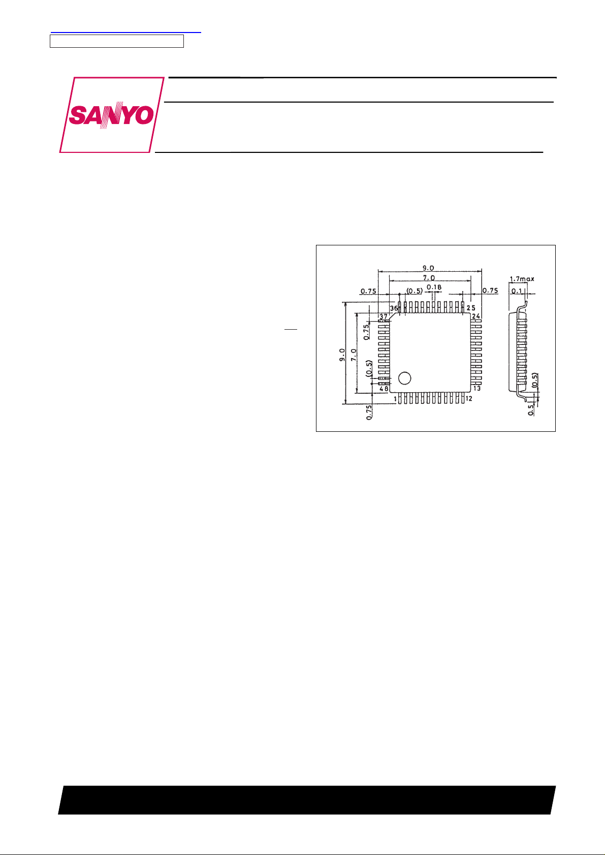
Package Dimensions
unit: mm
3163A-SQFP48
SANYO: SQFP48
[LC74FCT16245T, 74FCT162245T]
CMOS LSI
Ordering number : EN4627
63095HA (OT) No. 4627-1/8
SANYO Electric Co.,Ltd. Semiconductor Bussiness Headquarters
TOKYO OFFICE Tokyo Bldg., 1-10, 1 Chome, Ueno, Taito-ku, TOKYO, 110-8534 JAPAN
Fast 16-Bit CMOS Bidirectional Transceiver
LC74FCT16425T, 74FCT162245T
查询LC74FCT162245T供应商

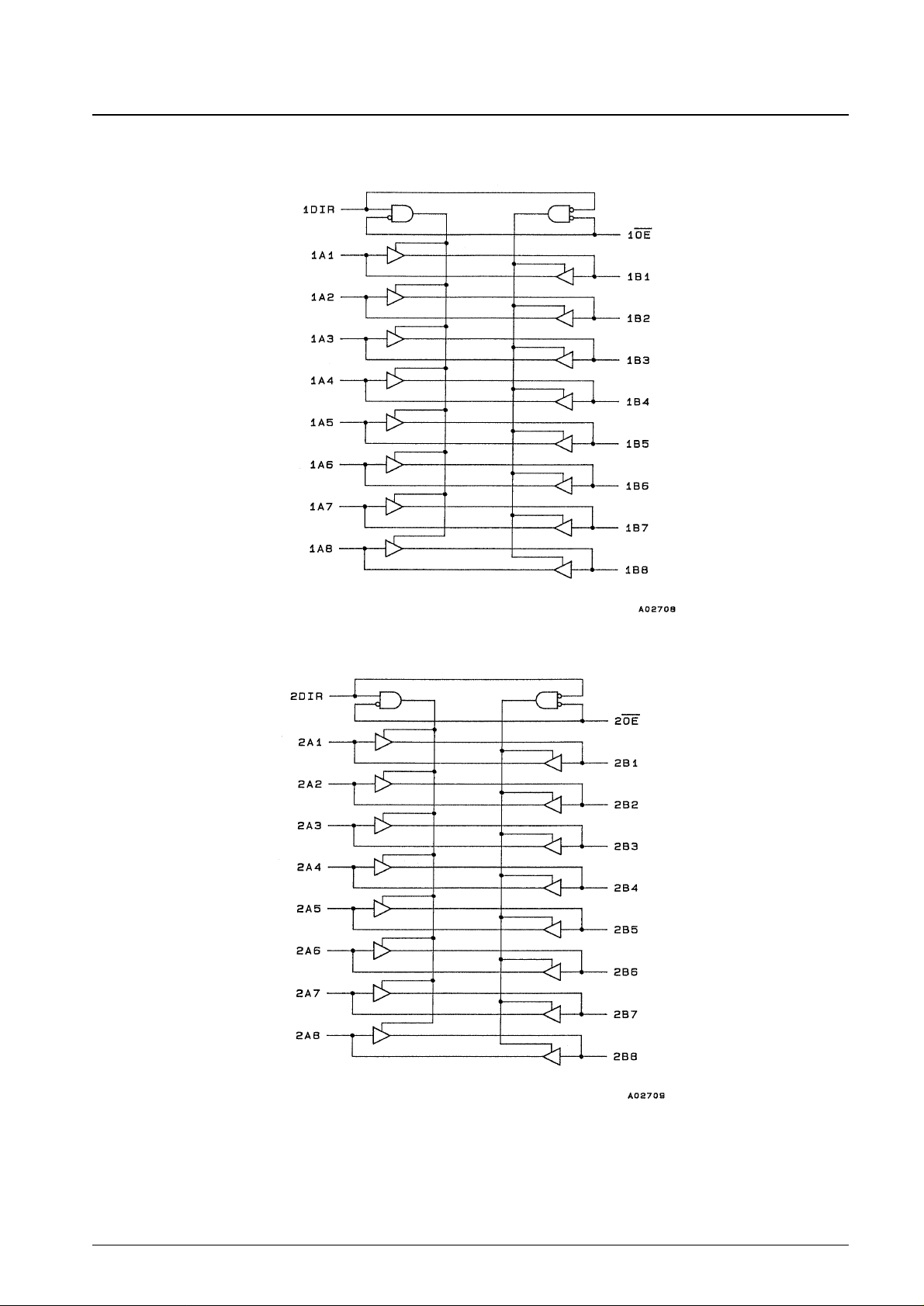
Function Block Diagram
No. 4627-2/8
LC74FCT16245T, 74FCT162245T

Pin Functions
Specifications
Absolute Maximum Ratings
*1
Note: 1. Applying stresses in excess of the absolute maximum ratings may permanently damage the device. The values specified here are stress ratings only,
and do not refer to operation under conditions outside either these conditions or the operating conditions. Operating for extended periods at the
absolute maximum ratings may adversely influence device reliability. Unless otherwise specified, pin voltages must not exceed V
CC
+ 0.5 V.
2. All pins except the FCT162xxxT output and I/O pins
3. All FCT162xxxT output and I/O pins
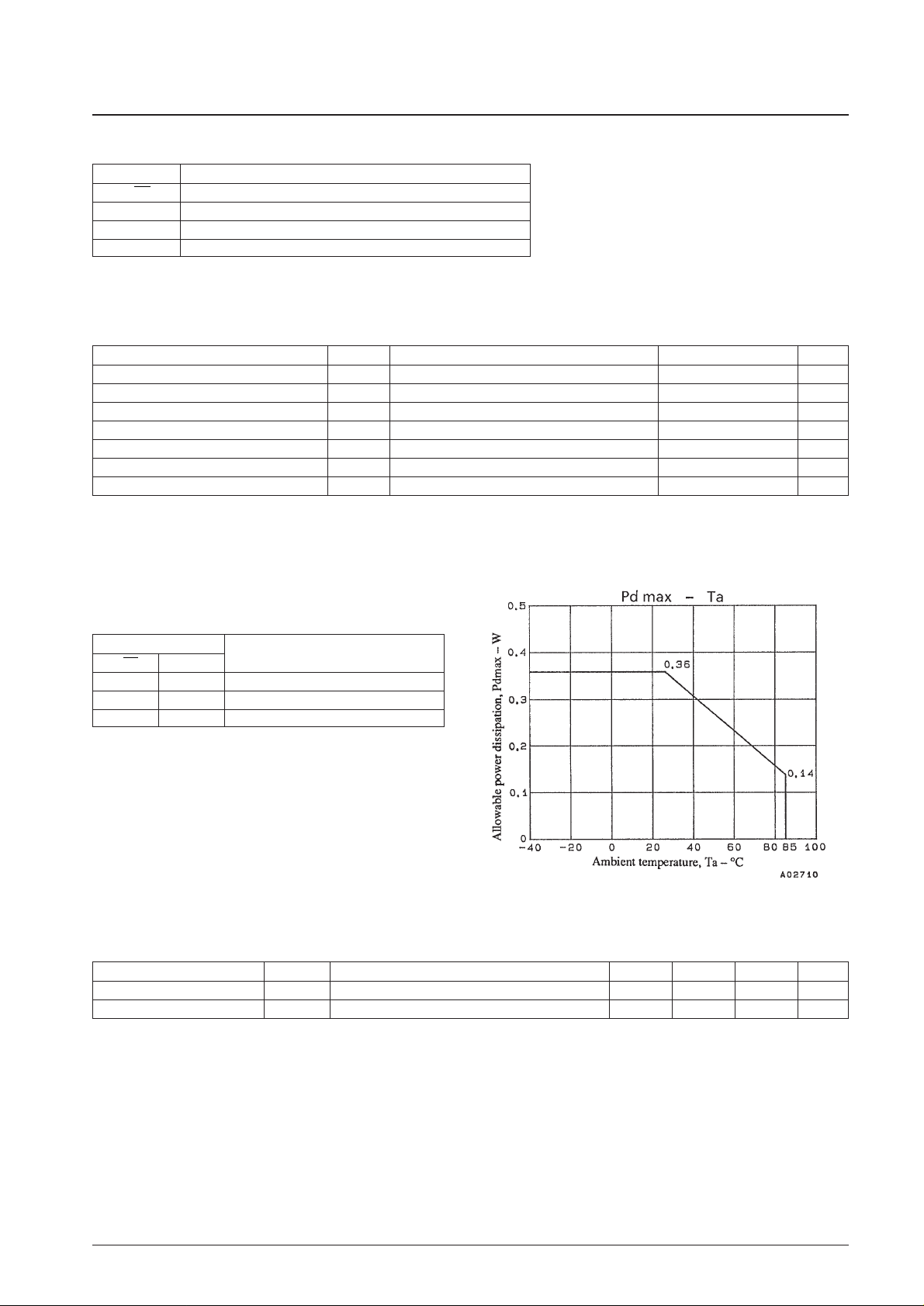
4. See Figure 1.
Function Truth Table*
Note: * H = High level
L = Low level
✕ = Don’t care
Figure 1
Capacitances (Ta = 25°C)
Note: * These capacitance values are logic values, and are not tested.
No. 4627-3/8
LC74FCT16245T, 74FCT162245T
Pin Function
× OE Output enable input (active low)
× DIR Direction control input
× AX A side input or three-state output
× BX B side input or three-state output
Input
Output
× OE × DIR
L L Bus B data output to bus A
L H Bus A data output to bus B
H ✕ High-impedance state.
Parameter Symbol Conditions Ratings Unit
Pin voltage referenced to GND V
TERM
*2
–0.5 to +7.0 V
Pin voltage referenced to GND V
TERM
*3
–0.5 to VCC+ 0.5 V
Operating temperature Topr –40 to +85 °C
Temperature when bias is applied T
BIAS
–55 to +125 °C
Storage temperature Tstg –55 to +125 °C
Power dissipation P
T
*4 W
DC output current I
OUT
–60 to +60 mA
Parameter* Symbol Conditions min typ max Unit
Input capacitance C
IN
5.5 8.0 pF
I/O capacitance C
I/O
4.5 6.0 pF
 Loading...