

Page 1
Ordering number : ENN1792D
2SK544
N-Channel Silicon MOSFET
2SK544
FM Tuner, VHF Amplifier Applications
Features
•
Low noise : NF=1.8dB typ (f=100MHz).
• High power gain : PG=27dB typ (f=100MHz).
• Small reverse transfer capacitance : Crss=0.035pF
(VDS=10V, f=1MHz).
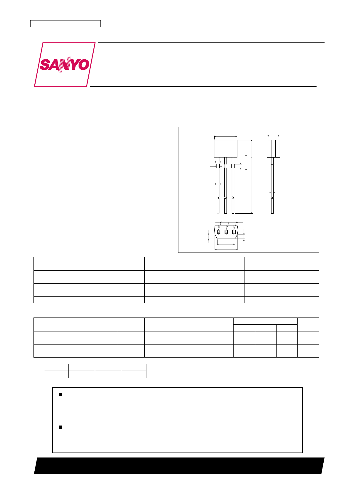
Package Dimensions
unit : mm
2040A
[2SK544]
4.0
0.4
0.5
0.6
0.4
123
1.3
1.3
2.2
3.0
1.8
15.0
0.4
1 : Drain
0.7
Specifications
Absolute Maximum Ratings at T a=25°C
Parameter Symbol Conditions Ratings Unit
Drain-to-Source Voltage V
Gate-to-Source Voltage V
Drain Current I
Allowable Power Dissipation P
Channel T emperature T ch 125 °C
Storage T emperature Tstg --55 to +150 °C
DS
GS
D
D
3.0
3.8nom
0.7
2 : Source
3 : Gate
SANYO : SPA
20 V
±5V
30 mA
300 mW
Electrical Characteristics at T a=25°C
Parameter Symbol Conditions
Drain-to-Source Voltage V
Gate-to-Source Leakage Current I
Zero-Gate Voltage Drain Current I
Cutoff Voltage VGS(off) VDS=10V , ID=100µA --2.5 V
* : The 2SK544 is classified by I
Rank D E F
I
DSS
1.2 to 3.0 2.5 to 6.0 5.0 to 12
as follows (unit : mA) :
DSS
DSX
GSS
DSS
VGS= --4V, ID=100µA20V
VDS=0, VGS=±5V 10 nA
*VDS=10V , VGS=0 1.2* 12* mA
min typ max
Any and all SANYO products described or contained herein do not have specifications that can handle
applications that require extremely high levels of reliability, such as life-support systems, aircraft's
control systems, or other applications whose failure can be reasonably expected to result in serious
physical and/or material damage. Consult with your SANYO representative nearest you before using
any SANYO products described or contained herein in such applications.
SANYO assumes no responsibility for equipment failures that result from using products at values that
exceed, even momentarily, rated values (such as maximum ratings, operating condition ranges, or other
parameters) listed in products specifications of any and all SANYO products described or contained
herein.
Ratings
Continued on next page.
SANYO Electric Co.,Ltd. Semiconductor Company
TOKYO OFFICE Tokyo Bldg., 1-10, 1 Chome, Ueno, Taito-ku, TOKYO, 110-8534 JAPAN
N1501 TS IM / 42899 TH (KT) / 6037 TA / 2075 KI, TS
No.1792-1/5
Unit
Page 2
2SK544
Continued from preceding page.
Parameter Symbol Conditions
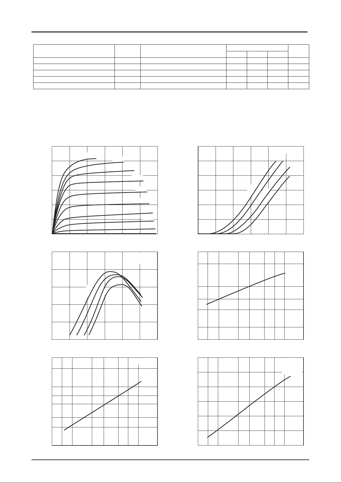
Forward Transfer Admittance
Input Capacitance Ciss VDS=10V, VGS=0, f=1MHz 2.4 pF
Reverse Transfer Capacitance Crss VDS=10V, VGS=0, f=1MHz 0.035 pF
Power Gain PG VDS=10V , VGS=0, f=100MHz 27 dB
Noise Figure NF See specified Test Circuit. 1.8 3.0 dB
yfs
VDS=10V , VGS=0, f=1kHz 11 mS
min typ max
Ratings
Unit
ID -- V
24
=1.2V
V
20
GS
DS
1.0V
0.8V
16
-- mA
D
12
8
Drain Current, I
4
0.6V
0.4V
0.2V
0V
--0.2V
--0.4V
0
024681012
Drain-to-Source V oltage, VDS -- V
20
|yfs| -- V
GS
ITR00819
VDS=10V
f=1kHz
-- mS
16
|
yfs
|
12
8
=10mA
DSS
I
8mA
5mA
3mA
ID -- V
DSS
I
GS
=10mA
8mA
5mA
3mA
-- mA
D
24
20
16
12
8
Drain Current, I
4
0
--1.5 --1.0 --0.5 0 0.5 1.0 1.5
Gate-to-Source V oltage, VGS -- V
-- mS
|
yfs
|
3
2
10
7
5
|yfs| -- I
D
VDS=10V
ITR00820
f=1kHz
4
Forward Transfer Admittance,
0
--
--
1.5 1.5
1.0
--
0.5
0.5 1.00
Gate-to-Source V oltage, VGS -- V
3
2
--
1.0
(off) -- V
7
GS
5
3
2
Cutoff Voltage, V
--
0.1
VGS(off) -- I
1.0
Drain Current, I
23 5757
DSS
DSS
-- mA
ITR00821
VDS=10V
10
ITR00823
3
Forward Transfer Admittance,
2
1.0
Drain Current, ID -- mA
16
|yfs| -- I
DSS
532
10
2757
ITR00822
VDS=10V
VGS=0
-- mS
|
yfs
|
14
12
10
8
6
f=1kHz
Forward Transfer Admittance,
2
4
1.0
Drain Current, I
DSS
532
-- mA
10
2757
ITR00824
No.1792-2/5
Page 3

Input Capacitance, Ciss -- pF
Reverse Transfer Capacitance, Crss -- pF
1.0
0.1
2SK544
10
5
3
2
5
3
2
5
3
2
Ciss, Crss -- V
Ciss
Crss
Drain-to-Source V oltage, V
10
7
5
3
2
Input Admittance yis -- V
c
DS
f=1MHz
VGS=0
-- mS
|
yfs
|
14
12
10
8
6
4
2
Forward Transfer Admittance,
16 201284024
DS
-- V
ITR00825
DS
VGS=0
f=100MHz
is
0
Drain-to-Source V oltage, VDS -- V
Reverse Transfer Admittance yrs -- V
5
3
2
|yfs| -- V
DS
VGS=0
f=1kHz
864201210
ITR00826
DS
VGS=0
f=100MHz
-- mS
is
g
-- mS
fs
g
1.0
7
-- pF
5
is
c
3
0.1
2
7
5
0
4
214
g
is
68
Drain-to-Source V oltage, V
Forward Transfer Admittance yfs -- V
5
3
2
g
fs
--b
fs
802 14121046
-- mS
fs
--b
10
7
5
3
2
1.0
Drain-to-Source V oltage, V
Input Admittance yis -- f
c
is
10
7
100
is
g
-- mS
is
g
1.0
0.1
5
3
2
7
5
3
2
7
5
3
2
7
Frequency, f -- MHz
10
DS
DS
I
D
-- V
-- V
=10mA
D
I
=10mA
0.7mA
12
ITR00827
DS
VGS=0
f=100MHz
ITR00829
VDS=10V
0.7mA
723 5 23 5
ITR00831
1000
0.1
-- pF
7
rs
5
--c
3
2
0.01
0 8 10 1221446
Drain-to-Source V oltage, V
Output Admittance yos -- V
0 8 10 1221446
-- µS
g
os
-- pF
os
c
10
7
5
3
2
1.0
7
5
3
2
0.1
7
5
Drain-to-Source V oltage, V
5
3
2
10
7
5
3
2
1.0
7
5
3
2
-- pF
is
c
S
µ
--
g
Reverse Transfer Admittance yrs -- f
3
2
100
7
I
=10mA
D
0.7mA
7
10
rs
5
3
2
10
7
5
3
2
1.0
--c
rs
c
os
g
os
--c
rs
=0.7mA
D
I
723 5 723 5
100 1000
Frequency, f -- MHz
DS
DS
10mA
-- V
DS
VGS=0
f=100MHz
-- V
VDS=10V
rs
g
ITR00828
ITR00830
ITR00832
3
2
0.1
7
5
3
2
0.01
7
5
3
2
0.001
pF
--
rs
--c
No.1792-3/5
Page 4

2SK544
Frequency, f -- MHz
Output Admittance yos -- f
g
os
-- mS
ITR00834
10
7
100
57 723 23 5
3
2
2
5
0.01
3
5
0.1
2
3
5
1.0
c
os
-- pF
3
2
2
5
1.0
3
5
2
3
5
10
100
c
os
g
os
Frequency, f -- MHz
Reverse Transfer Admittance yfs -- f
g
fs
--
m
S
ITR00833
10
7
100 1000
723 5 723 5
10
1.0
2
3
5
2
3
5
7
2
3
5
7
1.0
2
3
5
2
3
5
5
7
7
2
3
10
g
fs
--b
fs
VDS=10V
I
D
=10mA
5mA
--b
fs
-- mS
2mA
1mA
VDS=10V
I
D
=10mA
7mA
5mA
2mA
3mA
1mA
5mA
2mA
1mA
I
D
=10mA
I
D
=10mA
0.7mA
PG, NF -- I
D
Voltage Gain, PG -- dB
Noise Figure, NF -- dB
ITR00835
1.0
57
10
722335
0
2
4
14
18
22
26
30
34
PG
NF
Drain Current, ID -- mA
VDS=10V
f=100MHz
00 20 40 60 80 100 120 140 160
0
40
80
120
160
240
280
300
320
200
Ambient Temperature, Ta -- °C
P
D
-- Ta
Allowable Power Dissipation, P
D
-- mW
ITR00836
PG, NF Specified Test Circuit
Rg
50Ω
L1 : 1.0mmφ plated wire 10mmφ 6T, tap : 3T from H side
L2 : 1.0mmφ plated wire 10mmφ 7T, tap : 4T from H side
L1
to 30pF
to 20pF
V
G
to 20pF
L2
to 30pF
V
D
Unit(capacitance : F)
R
L
50Ω
No.1792-4/5
Page 5

2SK544
Specifications of any and all SANYO products described or contained herein stipulate the performance,
characteristics, and functions of the described products in the independent state, and are not guarantees
of the performance, characteristics, and functions of the described products as mounted in the customer's
products or equipment. To verify symptoms and states that cannot be evaluated in an independent device,
the customer should always evaluate and test devices mounted in the customer's products or equipment.
SANYO Electric Co., Ltd. strives to supply high-quality high-reliability products. However, any and all
semiconductor products fail with some probability. It is possible that these probabilistic failures could
give rise to accidents or events that could endanger human lives, that could give rise to smoke or fire,
or that could cause damage to other property. When designing equipment, adopt safety measures so
that these kinds of accidents or events cannot occur. Such measures include but are not limited to protective
circuits and error prevention circuits for safe design, redundant design, and structural design.
In the event that any or all SANYO products(including technical data,services) described or
contained herein are controlled under any of applicable local export control laws and regulations,
such products must not be exported without obtaining the export license from the authorities
concerned in accordance with the above law.
No part of this publication may be reproduced or transmitted in any form or by any means, electronic or
mechanical, including photocopying and recording, or any information storage or retrieval system,
or otherwise, without the prior written permission of SANYO Electric Co. , Ltd.
Any and all information described or contained herein are subject to change without notice due to
product/technology improvement, etc. When designing equipment, refer to the "Delivery Specification"
for the SANYO product that you intend to use.
Information (including circuit diagrams and circuit parameters) herein is for example only ; it is not
guaranteed for volume production. SANYO believes information herein is accurate and reliable, but
no guarantees are made or implied regarding its use or any infringements of intellectual property rights
or other rights of third parties.
This catalog provides information as of November, 2001. Specifications and information herein are subject
to change without notice.
No.1792-5/5
PS
 Loading...