

Page 1
Ordering number : ENN7169
Preliminary
2SK3557
N-Channel Junction Silicon FET
2SK3557
Low-Noise HF Amplifier Applications
Applications
•
AM tuner RF amplifier.
•
Low noise amplifier.
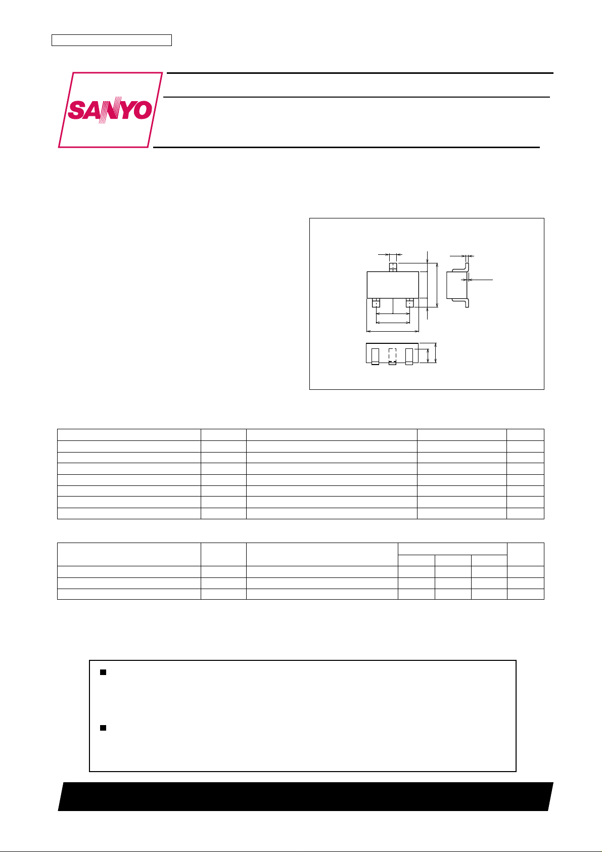
Package Dimensions
unit : mm
2050A
[2SK3557]
Features
•
Large yfs.
•
Small Ciss.
•
Ultrasmall-sized package permitting 2SK3557applied sets to be made smaller and slimer.
•
Ultralow noise figure.
0.4
3
0.95
0.95
1
2
1.9
2.9
0.5
2.5
1.5
0.5
1.1
0.8
0.16
0 to 0.1
1 : Source
2 : Drain
3 : Gate
SANYO : CP
Specifications
Absolute Maximum Ratings at Ta=25°C
Parameter Symbol Conditions Ratings Unit
Drain-to-Source Voltage V
Gate-to-Drain Voltage V
Gate Current I
Drain Current I
Allowable Power Dissipation P
Junction T emperature Tj 150 °C
Storage T emperature T stg --55 to +150 °C
DSX
GDS
G
D
D
15 V
--15 V
10 mA
50 mA
200 mW
Electrical Characteristics at Ta=25°C
Parameter Symbol Conditions
Gate-to-Drain Breakdown Voltage V
Gate Cutoff Current I
Cutoff Voltage VGS(off) VDS=5V, ID=100µA --0.3 --0.7 --1.5 V
Marking : IR Continued on next page.
(BR)GDSIG
GSS
=--10µA, VDS=0 --15 V
VGS=--10V, VDS=0 --1.0 nA
min typ max
Any and all SANYO products described or contained herein do not have specifications that can handle
applications that require extremely high levels of reliability, such as life-support systems, aircraft's
control systems, or other applications whose failure can be reasonably expected to result in serious
physical and/or material damage. Consult with your SANYO representative nearest you before using
any SANYO products described or contained herein in such applications.
SANYO assumes no responsibility for equipment failures that result from using products at values that
exceed, even momentarily, rated values (such as maximum ratings, operating condition ranges, or other
parameters) listed in products specifications of any and all SANYO products described or contained
herein.
Ratings
Unit
SANYO Electric Co.,Ltd. Semiconductor Company
TOKYO OFFICE Tokyo Bldg., 1-10, 1 Chome, Ueno, Taito-ku, TOKYO, 110-8534 JAPAN
60502 TS IM TA-3622
No.7169-1/4
Page 2
2SK3557
Continued from preceding page.
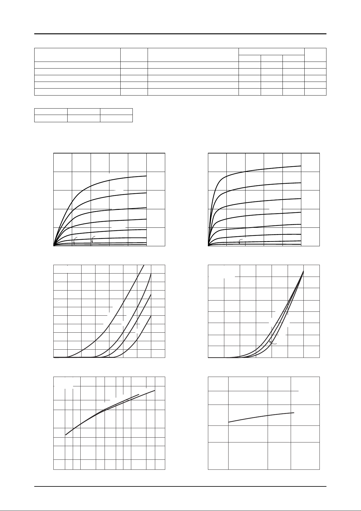
Parameter Symbol Conditions
Drain Current I
Forward Transfer Admittance
Input Capacitance Ciss VDS=5V, VGS=0, f=1MHz 10.0 pF
Reverse Transfer Capacitance Crss VDS=5V, VGS=0, f=1MHz 2.9 pF
Noise Figure NF VDS=5V, Rg=1kΩ, ID=1mA, f=1kHz 1.0 dB
DSS
yfs
VDS=5V, VGS=0 10* 32* mA
VDS=5V, VGS=0, f=1kHz 24 35 mS
Ratings
min typ max
Unit
*The 2SK3557 is classified by I
Rank 6 7
-- mA
D
I
DSS
20
16
12
8
10.0 to 20.0 16.0 to 32.0
as follows : (unit : mA)
DSS
I
-- V
D
DS
=0
V
GS
--0.1V
--0.2V
--0.3V
Drain Current, I
4
--0.7V
0
0.4 0.8 1.2 1.6 2.0 2.4
0
--0.6V
--0.4V
--0.5V
Drain-to-Source V oltage, VDS -- V
I
22
VDS=5V
20
18
16
14
-- mA
D
12
10
8
6
Drain Current, I
4
2
0
--1.4 --1.2 --1.0 --0.8 --0.6 --0.4 --0.2 0 0.2
D -- VGS
=30mA
DSS
I
20mA
15mA
Gate-to-Source V oltage, VGS -- V
7
V
=5V
DS
f=1kHz
5
yfs -- I
D
-- mS
3
yfs
2
I
DSS
=15mA
10mA
30mA
ITR02749
IT04224
I
-- V
20
16
D
DS
=0
V
GS
--0.1V
-- mA
12
D
--0.2V
8
Drain Current, I
4
--0.3V
--0.4V
--0.5V
0
0
24681012
--0.7V
--0.6V
Drain-to-Source V oltage, VDS -- V
I
16
VDS=5V
I
=15mA
DSS
14
12
10
-- mA
D
8
6
Drain Current, I
4
2
0
--1.2 --1.0 --0.8 --0.6 --0.4 --0.2 0 0.2
D -- VGS
Ta=--25°C
75°C
25°C
Gate-to-Source V oltage, VGS -- V
100
yfs -- I
7
5
DSS
ITR02750
ITR02752
VDS=5V
VGS=0
f=1kHz
10
7
5
3
Forward Transfer Admittance,
2
3
75235723
1.0
10
Drain Current, ID -- mA
5
IT04225
Forward Transfer Admittance, yfs -- mS
3
2
10
7
10
Drain Current, I
23 5
DSS
-- mA
IT04226
No.7169-2/4
Page 3

2SK3557
3
2
-- V
(off)
GS
1.0
7
5
Cutoff V oltage, V
3
10
7
-- pF
5
3
2
VGS(off) -- I
DSS
VDS=5V
3
ID=100µA
2
-- pF
10
7
5
Input Capacitance, Ciss
7
10
Drain Current, I
Crss -- V
23 5
DSS
-- mA
IT04227
DS
VDS=0
3
72357 23
1.0 10
10
f=1MHz
8
6
4
Ciss -- V
DS
Drain-to-Source V oltage, V
NF -- f
DS
-- V
VGS=0
f=1MHz
IT04228
VDS=5V
ID=1mA
Rg=1kΩ
1.0
7
Reverse Transfer Capacitance, Crss
5
73
1.0
10
2
Drain-to-Source V oltage, V
NF -- Rg
10
DS
-- V
2357
IT04229
VDS=5V
Noise Figure, NF -- dB
240
2
0
2
3 5 7 2 3 5 7 2 3 5 7 2 3 5 7
0.01
0.1 1.0 10
Frequency, f -- kHz
ID=1mA
8
f=1kHz
200
-- mW
D
6
4
160
120
80
Noise Figure, NF -- dB
2
40
Allowable Power Dissipation, P
0
2
3 5 7 2 3 5 7 2 3 5 7 2 3 5 7
0.1
1.0 10 100
Signal Source Resistance, Rg -- kΩ
1000
ITR02759 ITR02760
0
0 20 40 60 80 100 120 140 160
Ambient Temperature, Ta -- °C
100
ITR02758
PD -- Ta
No.7169-3/4
Page 4

2SK3557
Specifications of any and all SANYO products described or contained herein stipulate the performance,
characteristics, and functions of the described products in the independent state, and are not guarantees
of the performance, characteristics, and functions of the described products as mounted in the customer's
products or equipment. To verify symptoms and states that cannot be evaluated in an independent device,
the customer should always evaluate and test devices mounted in the customer's products or equipment.
SANYO Electric Co., Ltd. strives to supply high-quality high-reliability products. However, any and all
semiconductor products fail with some probability. It is possible that these probabilistic failures could
give rise to accidents or events that could endanger human lives, that could give rise to smoke or fire,
or that could cause damage to other property. When designing equipment, adopt safety measures so
that these kinds of accidents or events cannot occur. Such measures include but are not limited to protective
circuits and error prevention circuits for safe design, redundant design, and structural design.
In the event that any or all SANYO products(including technical data,services) described or
contained herein are controlled under any of applicable local export control laws and regulations,
such products must not be exported without obtaining the export license from the authorities
concerned in accordance with the above law.
No part of this publication may be reproduced or transmitted in any form or by any means, electronic or
mechanical, including photocopying and recording, or any information storage or retrieval system,
or otherwise, without the prior written permission of SANYO Electric Co. , Ltd.
Any and all information described or contained herein are subject to change without notice due to
product/technology improvement, etc. When designing equipment, refer to the "Delivery Specification"
for the SANYO product that you intend to use.
Information (including circuit diagrams and circuit parameters) herein is for example only ; it is not
guaranteed for volume production. SANYO believes information herein is accurate and reliable, but
no guarantees are made or implied regarding its use or any infringements of intellectual property rights
or other rights of third parties.
This catalog provides information as of June, 2002. Specifications and information herein are subject
to change without notice.
No.7169-4/4
PS
 Loading...