

SANYO 2SK3449 Datasheet
Ordering number : ENN6672
2SK3449
N-Channel Silicon MOSFET
2SK3449
DC / DC Converter Applications
Features
•
Low ON-resistance.
• Ultrahigh-speed switching.
• 4V drive.
Specifications
Absolute Maximum Ratings at Ta=25°C
Parameter Symbol Conditions Ratings Unit
Drain-to-Source Voltage V
Gate-to-Source Voltage V
Drain Current (DC) I
Drain Current (Pulse) I
Allowable Power Dissipation P
Channel T emperature T ch 150 °C
Storage T emperature Tstg --55 to +150 °C
DSS
GSS
D
DP
D
PW≤10µs, duty cycle≤1% 19.2 A
Tc=25°C10W
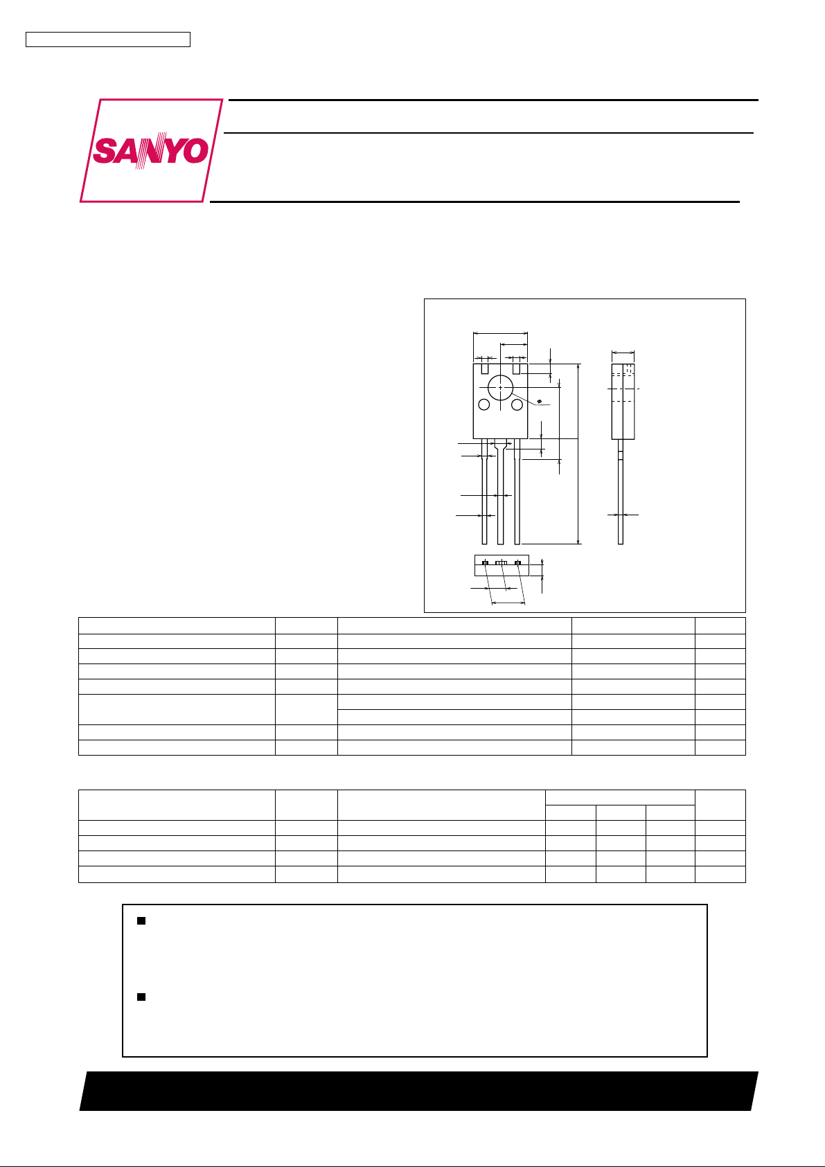
Package Dimensions
unit : mm
2190
[2SK3449]
8.0
4.0
1.0
1.6
0.8
0.8
0.75
2.4
1.0
1
2
4.8
1.4
3.0
11.0
7.5
1.5
3.0
15.5
3
1.7
3.3
0.7
1 : Source
2 : Drain
3 : Gate
SANYO : TO-126ML
60 V
±20 V
4.8 A
1W
Electrical Characteristics at Ta=25°C
Parameter Symbol Conditions
Drain-to-Source Breakdown Voltage V
Zero-Gate Voltage Drain Current I
Gate-to-Source Leakage Current I
Cutoff Voltage VGS(off) VDS=10V, ID=1mA 1.0 2.4 V
(BR)DSSID
DSS
GSS
=1mA, VGS=0 60 V
VDS=60V , VGS=0 10 µA
VGS=±16V, VDS=0 ±10 µA
Continued on next page.
Any and all SANYO products described or contained herein do not have specifications that can handle
applications that require extremely high levels of reliability, such as life-support systems, aircraft's
control systems, or other applications whose failure can be reasonably expected to result in serious
physical and/or material damage. Consult with your SANYO representative nearest you before using
any SANYO products described or contained herein in such applications.
SANYO assumes no responsibility for equipment failures that result from using products at values that
exceed, even momentarily, rated values (such as maximum ratings, operating condition ranges, or other
parameters) listed in products specifications of any and all SANYO products described or contained
herein.
Ratings
min typ max
SANYO Electric Co.,Ltd. Semiconductor Company
TOKYO OFFICE Tokyo Bldg., 1-10, 1 Chome, Ueno, Taito-ku, TOKYO, 110-8534 JAPAN
22201 TS IM TA-2919
No.6672-1/4
Unit
2SK3449
Continued from preceding page.
Parameter Symbol Conditions
Forward Transfer Admittance
Static Drain-to-Source On-State Resistance
Input Capacitance Ciss VDS=20V , f=1MHz 110 pF
Output Capacitance Coss VDS=20V , f=1MHz 35 pF
Reverse Transfer Capacitance Crss VDS=20V , f=1MHz 10 pF
Turn-ON Delay Time td(on) See specified Test Circuit 6 ns
Rise Time t
Turn-OFF Delay Time td(off) See specified Test Circuit 16 ns
Fall Time t
Total Gate Charge Qg VDS=10V, VGS=10V, ID=4.8A 4.5 nC
Gate-to-Source Charge Qgs VDS=10V, VGS=10V, ID=4.8A 0.9 nC
Gate-to-Drain “Miller” Charge Qgd VDS=10V, VGS=10V, ID=4.8A 0.8 nC
Diode Forward Voltage V
yfs
RDS(on)1 ID=2.4A, VGS=10V 240 320 mΩ
RDS(on)2 ID=2.4A, VGS=4V 320 440 mΩ
SD
VDS=10V, ID=2.4A 2.2 3.2 S
See specified Test Circuit 3.2 ns
r
See specified Test Circuit 4.8 ns
f
IS=4.8A, VGS=0 1 1.2 V
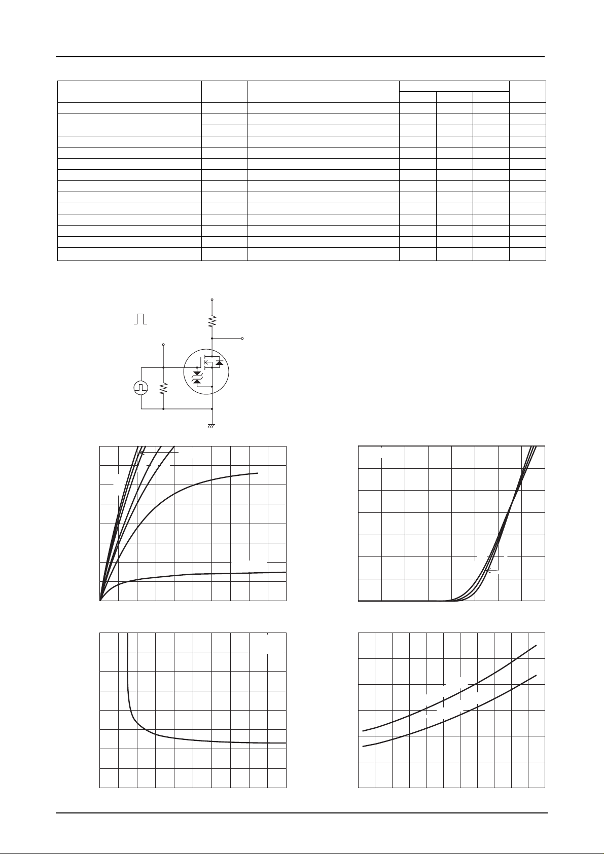
Switching Time Test Circuit
VDD=30V
V
10V
0V
PW=10µs
D.C.≤1%
IN
V
IN
G
D
ID=2.4A
RL=12.5Ω
V
OUT
Ratings
min typ max
Unit
P.G
1.6
1.4
1.2
5.0V
4.0V
3.5V
10.0V
-- A
1.0
D
0.8
0.6
Drain Current, I
0.4
0.2
0
0
0.4
Drain-to-Source V oltage, VDS -- V
800
700
600
(on) -- mΩ
500
DS
400
300
200
100
Static Drain-to-Source
On-State Resistance, R
0
024681012
RDS(on) -- V
Gate-to-Source V oltage, VGS -- V
I
50Ω
D
-- V
DS
S
2SK3449
8.0V
3.0V
=2.5V
V
GS
0.8 1.2 1.6 2.00.2 0.6 1.0 1.4 1.8
GS
Tc=25°C
ID=2.4A
14 16 18 20
IT01212
IT01214
I
-- V
3.5
VDS=10V
3.0
2.5
-- A
D
2.0
1.5
1.0
Drain Current, I
0.5
0
0 0.5 1.0 1.5 2.0 2.5 3.0 4.03.5
D
Gate-to-Source V oltage, VGS -- V
600
500
400
(on) -- mΩ
DS
300
200
100
Static Drain-to-Source
On-State Resistance, R
0
- -60
- -40 - -20 0 20 40 60 80 100 120 140 160
RDS(on) -- Tc
GS
=2.4A, V
I
D
=2.4A, V
I
D
Case Temperature, Tc -- °C
GS
=4V
GS
Tc=75°C
- -25°C
=10V
25°C
IT01213
IT01215
No.6672-2/4
 Loading...