

SANYO 2SK3293 Datasheet
Any and all SANYO products described or contained herein do not have specifications that can handle
applications that require extremely high levels of reliability, such as life-support systems, aircraft’s
control systems, or other applications whose failure can be reasonably expected to result in serious
physical and/or material damage. Consult with your SANYO representative nearest you before using
any SANYO products described or contained herein in such applications.
SANYO assumes no responsibility for equipment failures that result from using products at values that
exceed, even momentarily, rated values (such as maximum ratings, operating condition ranges,or other
parameters) listed in products specifications of any and all SANYO products described or contained
herein.
N-Channel Silicon MOSFET
Ultrahigh-Speed Switching Applications
Ordering number:ENN6345
2SK3293
SANYO Electric Co.,Ltd. Semiconductor Company
TOKYO OFFICE Tokyo Bldg., 1-10, 1 Chome, Ueno, Taito-ku, TOKYO, 110-8534 JAPAN
4.5
Features
· Low ON resistance.
· Ultrahigh-speed switching.
· 4V drive.
Specifications
Absolute Maximum Ratings at Ta = 25˚C
retemaraPlobmySsnoitidnoCsgnitaRtinU
egatloVecruoS-ot-niarDV
egatloVecruoS-ot-etaGV
)CD(tnerruCniarDI
)esluP(tnerruCniarDI
noitapissiDrewoPelbawollAP
erutarepmeTlennahChcT 051
erutarepmeTegarotSgtsT 051+ot55–
D
D
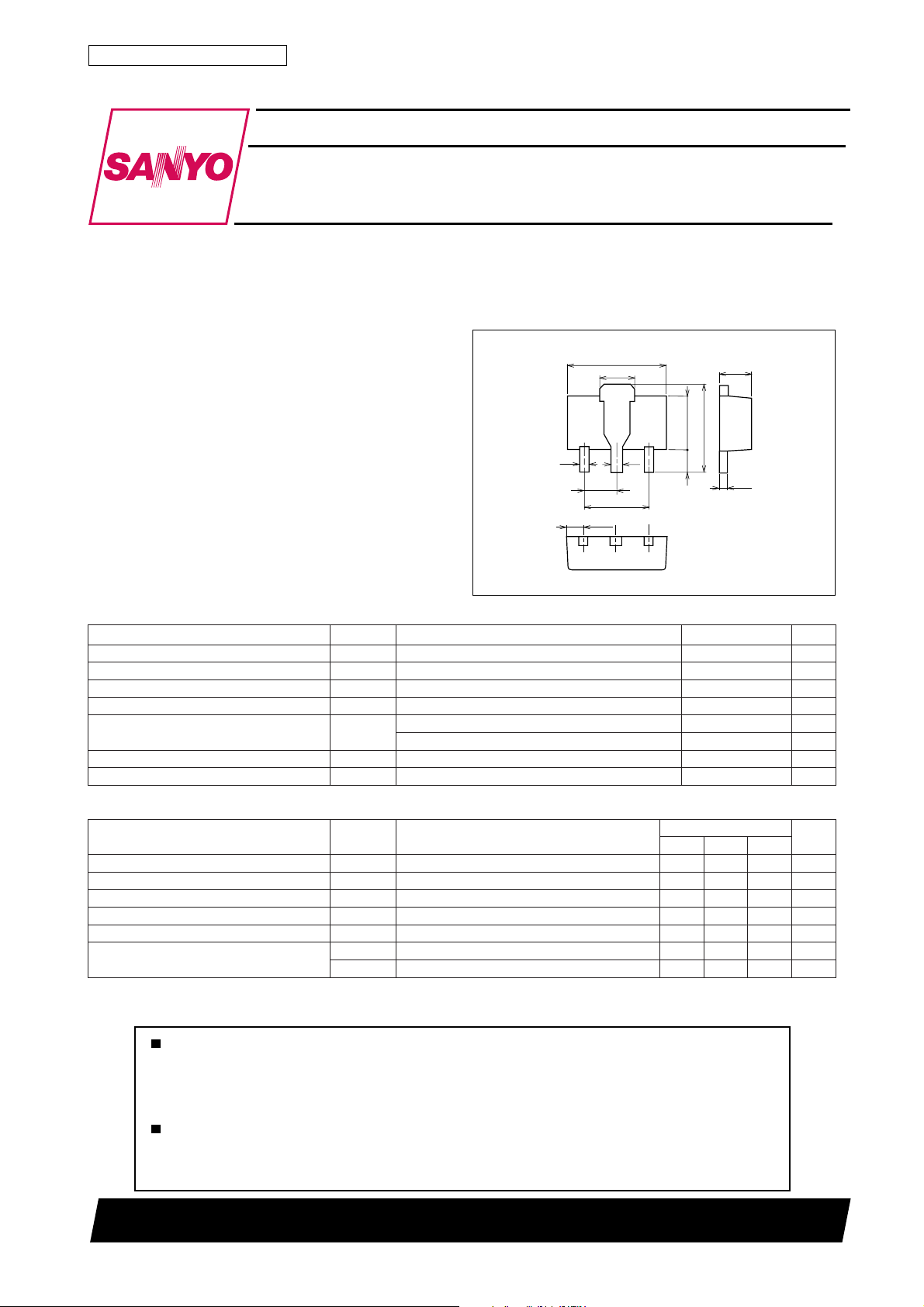
Package Dimensions
unit:mm
2062A
SSD
SSG
PW≤10µs, duty cycle≤1%
PD
Mounted on a ceramic board (250mm2×0.8mm)
Tc=25˚C
[2SK3293]
1.6
0.4
0.5
2
3
1.5
0.75
1
3.0
1.5
2.5
4.25max
1.0
0.4
1 : Gate
2 : Drain
3 : Source
SANYO : PCP
(Bottom view)
06V
02±V
3A
21A
5.1W
5.3W
˚C
˚C
Electrical Characteristics at Ta = 25˚C
retemaraPlobmySsnoitidnoC
egatloVnwodkaerBecruoS-ot-niarDV
tnerruCniarDegatloVetaGoreZI
tnerruCegakaeLecruoS-ot-etaGI
egatloVffotuCV
ecnattimdArefsnarTdrawroF|sfy|VSDI,V01=
R
ecnatsiseRetatS-nOecruoS-ot-niarDcitatS
R
SG
SD
SD
SSD)RB(
SSD
SSG
)ffo(VSDI,V01=
1)no(IDV,A5.1=
2)no(IDV,A1=
I
V,Am1=
D
V
SD
V
SG
0=06V
SG
V,V06=
0=01Aµ
SG
V,V61±=
0=01±Aµ
SD
Am1=0.14.2V
D
A5.1=6.26.3S
D
V01=511051mΩ
SG
V4=051012mΩ
SG
nimpytxam
Marking : KZ Continued on next page.
60800TS (KOTO) TA-2737 No.6345–1/4
sgnitaR
tinU
2SK3293
Continued from preceding page.
retemaraPlobmySsnoitidnoC
ecnaticapaCtupnIssiCV
ecnaticapaCtuptuOssoCV
ecnaticapaCrefsnarTesreveRssrCV
emiTyaleDNO-nruTt
emiTesiRt
emiTyaleDFFO-nruTt
emiTllaFt
egrahCetaGlatoTgQ
egrahCecruoS-ot-etaGsgQ 3.1Cn
egrahC"relliM"niarD-ot-etaGdgQ 8.1Cn
egatloVdrawroFedoiDV
r
f
DS
SD
SD
SD
)no(d
)ffo(d
V
SD
I
V,A3=
S
Switching Time Test Circuit
V
10V
0V
PW=10µs
D.C.≤1%
IN
V
VDD=30V
ID=1.5A
IN
G
RL=20Ω
D
V
OUT
zHM1=f,V02=022Fp
zHM1=f,V02=57Fp
zHM1=f,V02=52Fp
tiucriCtseTdeificepseeS7sn
tiucriCtseTdeificepseeS8sn
tiucriCtseTdeificepseeS03sn
tiucriCtseTdeificepseeS92sn
V,V01=
SG
I,V01=
SG
D
0=38.02.1V
sgnitaR
nimpytxam
6.8Cn
A3=
tinU
2SK3293
S
DS
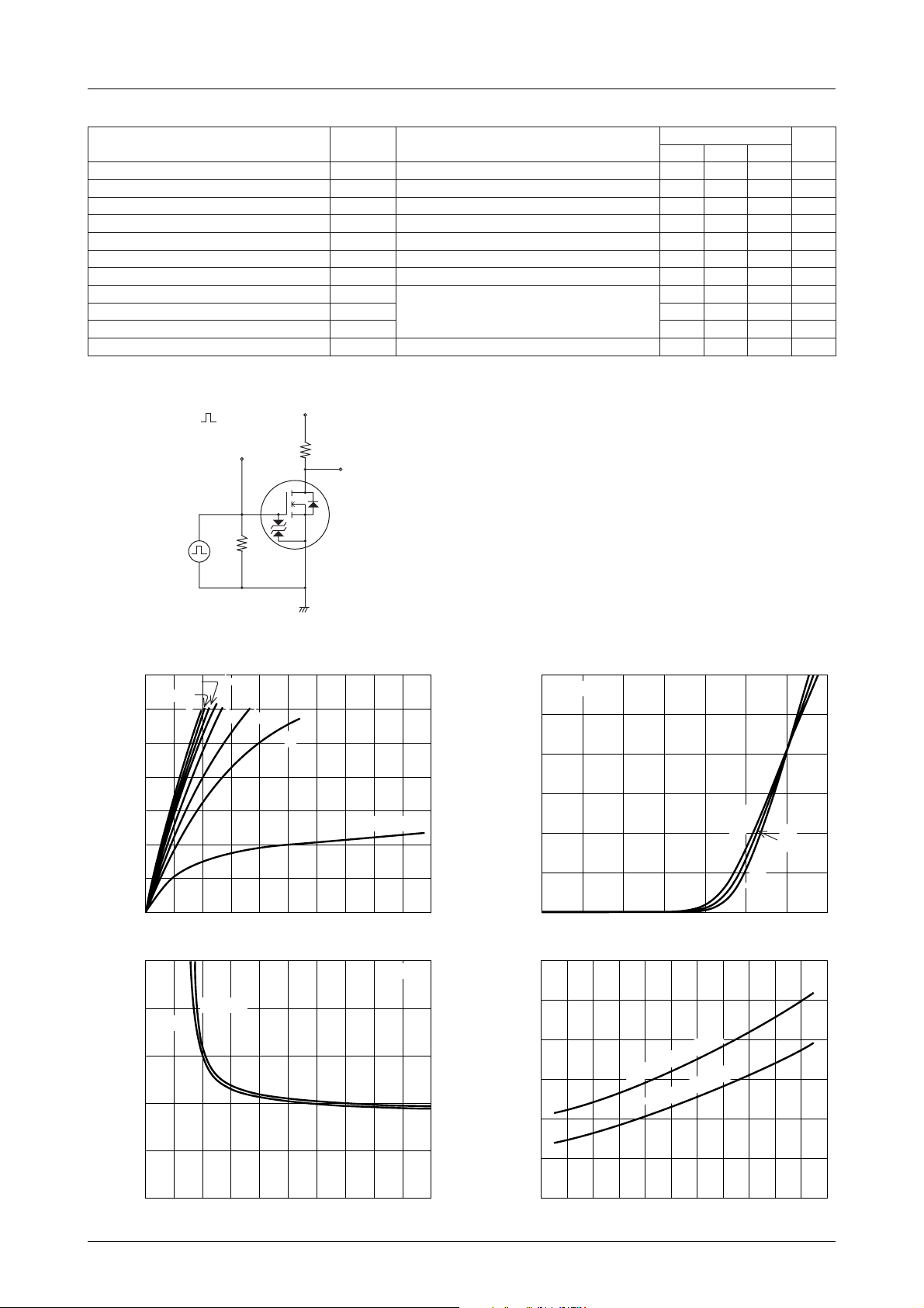
3.5
3.0
2.5
–A
D
2.0
1.5
P.G
8.0V
6.0V
10.0V
5.0V
4.0V
50Ω
I
D
3.5V
-- V
3.0V
VGS=2.5V
1.0
Drain Current, I
0.5
0
0 0.2 0.4 0.6 0.8 1.0 1.2 1.4 1.6 1.8 2.0
Drain-to-Source Voltage, VDS –V
250
RDS(on) -- V
GS
Tc=25°C
I
-- V
6
D
GS
VDS=10V
5
4
–A
D
3
2
Drain Current, I
1
Tc=75°C
25°C
--25°C
0
IT01457 IT01458
0 0.5 1.0 1.5 2.0 2.5 3.0
300
Gate-to-Source Voltage, VGS –V
RDS(on) -- Tc
3.5
mΩ
200
(on) –
DS
150
100
50
Static Drain-to-Source
On-State Resistance, R
0
024681012141618
ID=1.5A
1.0A
Gate-to-Source Voltage, VGS –V
IT01459
mΩ
250
(on) –
200
DS
=1.0A, V
I
150
100
50
Static Drain-to-Source
On-State Resistance, R
20
0
--60 --40 --20 0 20 40 60 80 100 120
D
I
D
Case Temperature, Tc – °C
GS
=1.5A, V
=4V
GS
=10V
160140
IT01460
No.6345–2/4
 Loading...