

SANYO 2SK2775 Datasheet
Any and all SANYO products described or contained herein do not have specifications that can handle
applications that require extremely high levels of reliability, such as life-support systems, aircraft’s
control systems, or other applications whose failure can be reasonably expected to result in serious
physical and/or material damage. Consult with your SANYO representative nearest you before using
any SANYO products described or contained herein in such applications.
SANYO assumes no responsibility for equipment failures that result from using products at values that
exceed, even momentarily, rated values (such as maximum ratings, operating condition ranges,or other
parameters) listed in products specifications of any and all SANYO products described or contained
herein.
N-Channel Silicon MOSFET
Ultrahigh-Speed Switching Applications
Ordering number:ENN6392
2SK2775
SANYO Electric Co.,Ltd. Semiconductor Company
TOKYO OFFICE Tokyo Bldg., 1-10, 1 Chome, Ueno, Taito-ku, TOKYO, 110-8534 JAPAN
Features
· Low ON resistance.
· Ultrahigh-speed switching.
· 4V drive.
· Enables simplified fabrication, high-density mounting, and miniaturization in end products due to the
surface mountable package.
Specifications
Absolute Maximum Ratings at Ta = 25˚C
retemaraPlobmySsnoitidnoCsgnitaRtinU
egatloVecruoS-ot-niarDV
egatloVecruoS-ot-etaGV
)CD(tnerruCniarDI
)esluP(tnerruCniarDI
noitapissiDrewoPelbawollAP
erutarepmeTlennahChcT 051
erutarepmeTegarotSgtsT 051+ot55–
SSD
SSG
D
PD
D
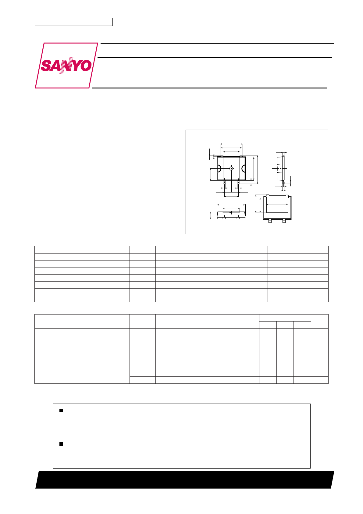
Package Dimensions
unit:mm
2128
PW≤10µs, duty cycle≤1%
Tc=25°C
[2SK2775]
8.2
7.8
0.4
4.2
2.5
6.2
0.2
3
8.4
1.2
2
1.0
2.54
6.2
1.0
2.54
1
5.08
10.0
6.0
10.0
0.6
0.7
0.3
0.6
7.8
5.2
1 : Gate
2 : Source
3 : Drain
SANYO : ZP
(Bottom view)
001V
02±V
52A
001A
04W
˚C
˚C
Electrical Characteristics at Ta = 25˚C
retemaraPlobmySsnoitidnoC
egatloVnwodkaerBecruoS-ot-niarDV
egatloVnwodkaerBecruoS-ot-etaGV
tnerruCniarDegatloVetaG-oreZI
tnerruCegakaeLecruoS-ot-etaGI
egatloVffotuCV
ecnattimdArefsnarTdrawroF|sfy|VSDI,V01=
R
ecnatsiseRetatS-nOecruoS-ot-niarDcitatS
R
I
V,Am1=
SSD)RB(
D
I
SSG)RB(
G
V
SSD
SSG
SD
SD
V
V
)ffo(SG
1)no(IDV,V21=
2)no(IDV,V21=
SD
SG
SD
0=001V
SG
V,Aµ001±=
0=02±V
SG
V,V001=
0=001Aµ
SG
V,V61±=
0=01±Aµ
SD
I,V01=
Am1=0.10.2V
D
A21=515.42S
D
V01=0608mΩ
SG
V4=08011mΩ
SG
60800TS (KOTO) TA-2760 No.6392–1/4
sgnitaR
nimpytxam
Continued on next page.
tinU
2SK2775
Continued from preceding page.
retemaraPlobmySsnoitidnoC
ecnaticapaCtupnIssiCV
ecnaticapaCtuptuOssoCV
ecnaticapaCrefsnarTesreveRssrCV
emiTyaleDNO-nruTt
emiTesiRt
emiTyaleDFFO-nruTt
emiTllaFt
egatloVdrawroFedoiDV
r
f
DS
SD
SD
SD
)no(d
)ffo(d
I
S
zHM1=f,V02=0091Fp
zHM1=f,V02=003Fp
zHM1=f,V02=06Fp
tiucriCtseTdeificepseeS51sn
tiucriCtseTdeificepseeS02sn
tiucriCtseTdeificepseeS092sn
tiucriCtseTdeificepseeS001sn
V,A52=
0=0.15.1V
SG
sgnitaR
nimpytxam
tinU
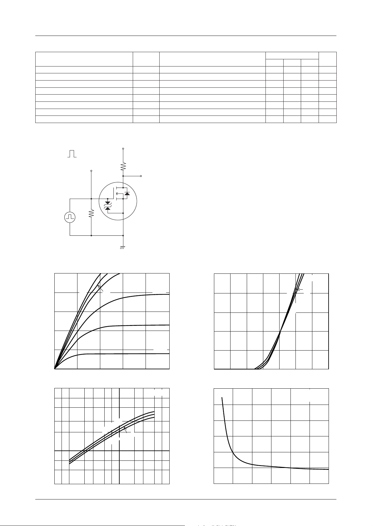
Switching Time Test Circuit
V
IN
10V
0V
V
GS
V
IN
=5.0V
G
50Ω
I
D
-- V
4.0V
4.5V
50
40
–A
D
30
20
PW=10µs
D.C.≤1%
P.G
VDD=50V
D
S
DS
ID=12A
RL=4.17Ω
V
2SK2775
OUT
3.5V
3.0V
50
40
–A
D
30
20
I
D
-- V
GS
Tc= --25
°C
75°C
VDS=10V
°C
25
Drain Current, I
10
0
0
100
7
5
fs|–S
y
3
2
24 8106
Drain-to-Source Voltage, VDS–V
y
fs -- I
T
= --25°C
C
D
2.5V
IT00690 IT00691
VDS=10V
25°C
10
7
5
Forward Transfer Admittance, |
3
1.0
27773355
75°C
Drain Current, ID–A
10
25
100
IT00692 IT00693
Drain Current, I
10
0
0
160
140
–mΩ
120
(on)
DS
100
80
60
Static Drain-to-Source
On-State Resistance, R
40
Gate-to-Source Voltage, VGS–V
Gate-to-Source Voltage, V
2135
RDS(on) -- V
GS
64
Tc=25°C
ID=12A
8212146104
GS
–V
7
No.6392–2/4
 Loading...