

SANYO 2SK2624LS Datasheet
Any and all SANYO products described or contained herein do not have specifications that can handle
applications that require extremely high levels of reliability, such as life-support systems, aircraft’s
control systems, or other applications whose failure can be reasonably expected to result in serious
physical and/or material damage. Consult with your SANYO representative nearest you before using
any SANYO products described or contained herein in such applications.
SANYO assumes no responsibility for equipment failures that result from using products at values that
exceed, even momentarily, rated values (such as maximum ratings, operating condition ranges,or other
parameters) listed in products specifications of any and all SANYO products described or contained
herein.
N-Channel Silicon MOSFET
Ultrahigh-Speed Switching Applications
Ordering number:ENN5404B
2SK2624LS
SANYO Electric Co.,Ltd. Semiconductor Company
TOKYO OFFICE Tokyo Bldg., 1-10, 1 Chome, Ueno, Taito-ku, TOKYO, 110-8534 JAPAN
4.5
Features
· Low ON-resistance.
· Low Qg.
Specifications
Absolute Maximum Ratings at Ta = 25˚C
retemaraPlobmySsnoitidnoCsgnitaRtinU
egatloVecruoS-ot-niarDV
egatloVecruoS-ot-etaGV
)CD(tnerruCniarDI
)esluP(tnerruCniarDI
noitapissiDrewoPelbawollAP
erutarepmeTlennahChcT 051
erutarepmeTegarotSgtsT 051+ot55–
D
D
SSD
SSG
PD
PW≤10µs, duty cycle≤1%
Tc=25˚C
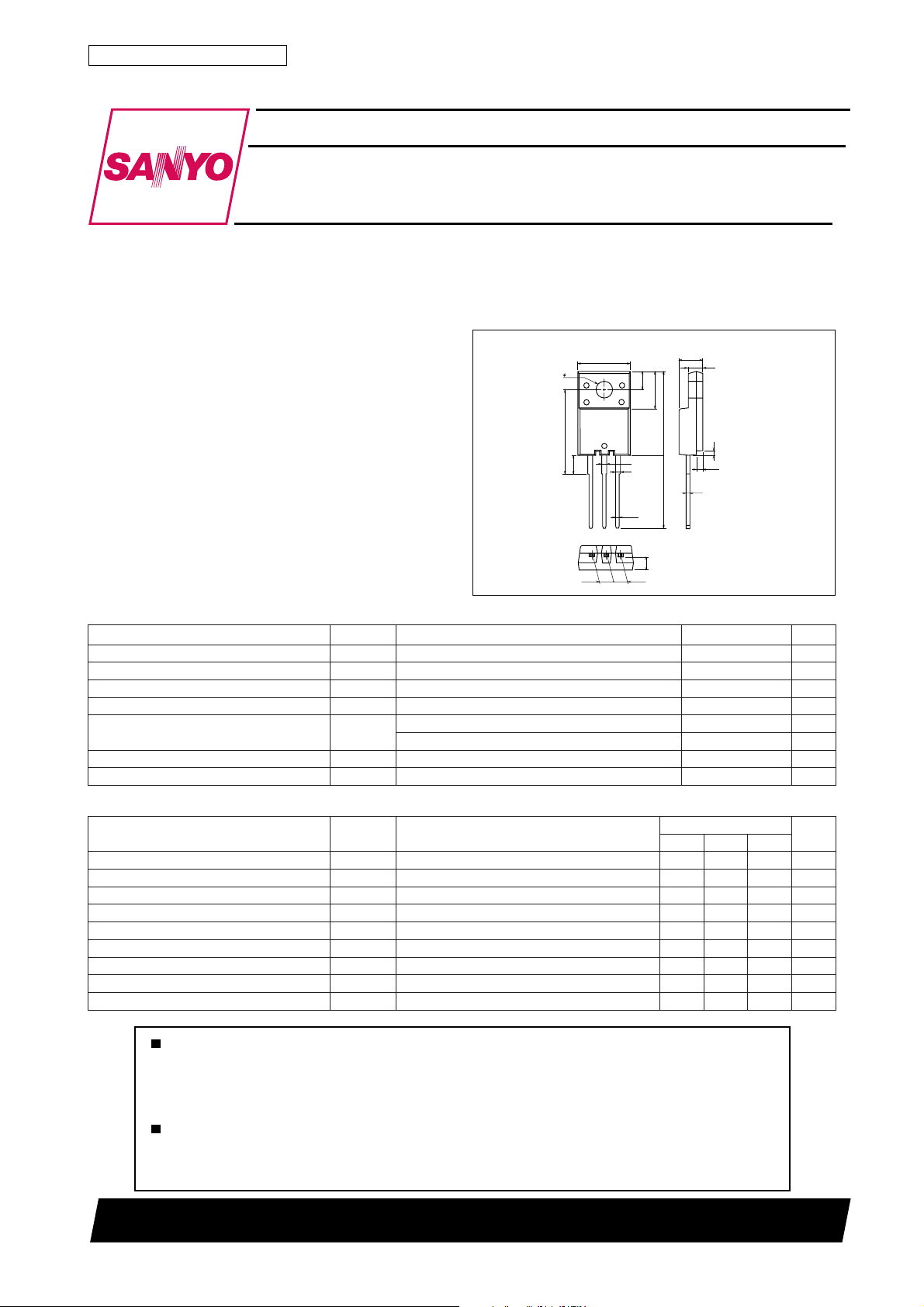
Package Dimensions
unit:mm
2078B
[2SK2624LS]
10.0
3.2
16.1
3.6
123
3.5
7.2
0.9
1.2
0.75
2.4
2.552.55
16.0
14.0
2.8
0.6
1.2
0.7
1 : Gate
2 : Drain
3 : Source
SANYO : TO220FI-LS
006V
03±V
3A
21A
0.2W
52W
˚C
˚C
Electrical Characteristics at Ta = 25˚C
retemaraPlobmySsnoitidnoC
egatloVnwodkaerBecruoS-ot-niarDV
tnerruCniarDegatloVetaG-oreZI
tnerruCegakaeLecruoS-ot-etaGI
egatloVffotuCV
ecnattimdArefsnarTdrawroF|sfy|VSDI,V01=
ecnatsiseRetatS-nOecruoS-ot-niarDcitatSR
ecnaticapaCtupnIssiCV
ecnaticapaCtuptuOssoCV
ecnaticapaCrefsnarTesreveRssrCV
SSD
SSG
SG
SD
I
SSD)RB(
D
V
SD
V
SG
)ffo(VSDI,V01=
)no(VSGI,V51=
SD
SD
SD
V,Am1=
0=006V
SG
V,V006=
0=0.1Am
SG
V,V03±=
0=001±An
SD
Am1=5.35.5V
D
A8.1=0.10.2S
D
A8.1=0.26.2
D
zHM1=f,V02=055Fp
zHM1=f,V02=561Fp
zHM1=f,V02=58Fp
N2000TS (KOTO) TA-2884 No.5404–1/4
sgnitaR
nimpytxam
Continued on next page.
tinU
Ω
2SK2624LS
Continued from preceding page.
retemaraPlobmySsnoitidnoC
egrahCetaGlatoTgQVSDV,V002=
emiTyaleDNO-nruTt
emiTesiRt
emiTyaleDFFO-nruTt
emiTllaFt
egatloVdrawroFedoiDV
)no(d
r
)ffo(d
f
I
V,A3=
DS
S
0=89.02.1V
SG
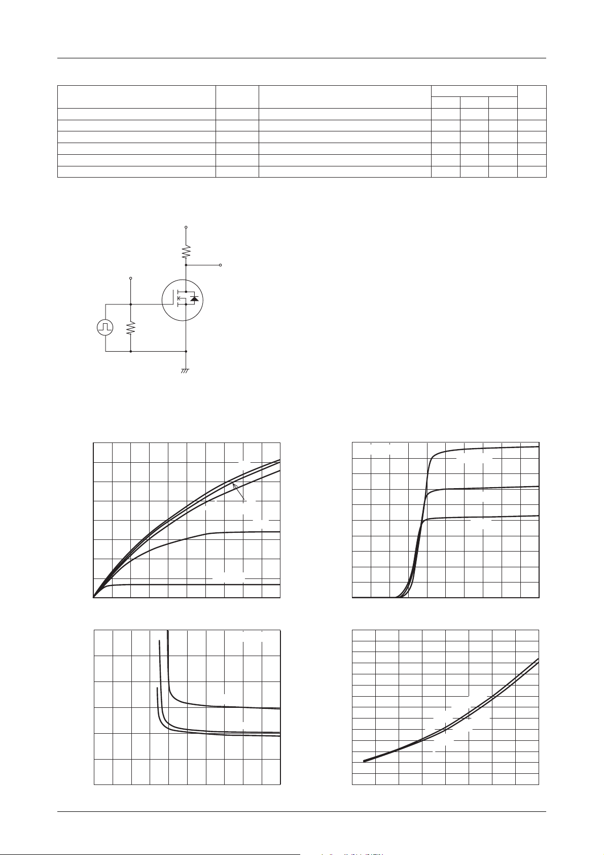
Switching Time Test Circuit
VDD=200V
ID=1.8A
RL=111Ω
V
2SK2624LS
OUT
PW=1µs
D.C.≤0.5%
P.G
VGS=15V
G
R
GS
50Ω
D
S
I,V01=
SG
D
tiucriCtseTdeificepseeS71sn
tiucriCtseTdeificepseeS71sn
tiucriCtseTdeificepseeS04sn
tiucriCtseTdeificepseeS22sn
sgnitaR
nimpytxam
A3=51Cn
tinU
4.0
3.5
3.0
–A
2.5
D
2.0
1.5
Drain Current, I
1.0
0.5
0
4.0
3.5
– Ω
3.0
(on)
DS
2.5
2.0
1.5
Static Drain-to-Source
On-State Resistance, R
1.0
0
24 810613 795
Drain-to-Source Voltage, VDS–V
Gate-to-Source Voltage, V
I
-- V
D
DS
RDS(on) -- V
82122014 16 186104
8V
VGS=6V
GS
ID=3.0A
1.8A
1.0A
–V
GS
I
-- V
D
=1.8A, V
I
D
=1.8A, V
I
D
50--25 15025 75 100 1250
GS
Tc=--25°C
25°C
75°C
=10V
GS
=15V
GS
5.0
VDS=10V
15V
10V
7V
IT01020 IT01021
Tc=25°C
IT01022
4.5
4.0
3.5
–A
D
3.0
2.5
2.0
1.5
Drain Current, I
1.0
0.5
00
0
2 6 12 14 16 18108204
Gate-to-Source Voltage, VGS–V
7.0
6.5
6.0
5.5
– Ω
5.0
4.5
(on)
DS
4.0
3.5
3.0
2.5
2.0
1.5
1.0
Static Drain-to-Source
On-State Resistance, R
0.5
0
--5 0
RDS(on) -- Tc
Case Temperature, Tc – ˚C
IT01023
No.5404–2/4
 Loading...