SANYO 2SK2379 Datasheet

SANYO Electric Co.,Ltd. Semiconductor Company
TOKYO OFFICE Tokyo Bldg., 1-10, 1 Chome, Ueno, Taito-ku, TOKYO, 110-8534 JAPAN
Ordering number : ENN5374A
2SK2379
N-Channel Silicon MOSFET
2SK2379
Ultrahigh-Speed Switching Applications
Features
•
Low ON-resistance.
• Ultrahigh-speed switching.
• Low-voltage drive.
• Micalless package facilitaing mounting.
Specifications
Package Dimensions
unit : mm
2063A
[2SK2379]
10.0
3.2
18.1
5.6
1
2.55
2.55
1.6
23
2.55
1.2
0.75
2.55
3.5
7.2
16.0
14.0
2.4
4.5
2.8
2.4
0.7
1 : Gate
2 : Drain
3 : Source
SANYO : TO-220ML
Absolute Maximum Ratings at T a=25°C
Parameter Symbol Conditions Ratings Unit
Drain-to-Source Voltage V
Gate-to-Source Voltage V
Drain Current (DC) I
Drain Current (Pulse) I
Allowable Power Dissipation P
Channel T emperature T ch 150 °C
Storage Temperature Tstg --55 to +150 °C
DSS
GSS
D
DP
D
PW≤10µs, duty cycle≤1% 80 A
Tc=25°C40W
200 V
±20 V
20 A
2.0 W
Electrical Characteristics at T a=25°C
Parameter Symbol Conditions
Drain-to-Source Breakdown Voltage V
Gate-to-Source Breakdown Voltage V
Zero-Gate Voltage Drain Current I
Gate-to-Source Leakage Current I
Cutoff Voltage VGS(off) VDS=10V, ID=1mA 1.5 2.5 V
Forward Transfer Admittance |yfs| VDS=10V, ID=10A 9.5 16 S
(BR)DSSID
(BR)GSSIG
DSS
GSS
=1mA, VGS=0 200 V
=±100µA, VDS=0 ±20 V
VDS=200V, VGS=0 100 µA
VGS=±16V, VDS=0 ±10 µA
Any and all SANYO products described or contained herein do not have specifications that can handle
applications that require extremely high levels of reliability, such as life-support systems, aircraft's
control systems, or other applications whose failure can be reasonably expected to result in serious
physical and/or material damage. Consult with your SANYO representative nearest you before using
any SANYO products described or contained herein in such applications.
SANYO assumes no responsibility for equipment failures that result from using products at values that
exceed, even momentarily, rated values (such as maximum ratings, operating condition ranges, or other
parameters) listed in products specifications of any and all SANYO products described or contained
herein.
Ratings
min typ max
Continued on next page.
D2500 TS IM TA-3128
No.5374-1/4
Unit

2SK2379
Continued from preceding page.
Parameter Symbol Conditions
Static Drain-to-Source On-State Resistance RDS(on) ID=10A, VGS=10V 70 95 mΩ
Input Capacitance Ciss VDS=20V , f=1MHz 2400 pF
Output Capacitance Coss VDS=20V , f=1MHz 500 pF
Reverse Transfer Capacitance Crss VDS=20V , f=1MHz 200 pF
Turn-ON Delay Time td(on) See specified Test Circuit 35 ns
Rise Time t
Turn-OFF Delay Time td(off) See specified Test Circuit 710 ns
Fall Time t
Diode Forward Voltage V
r
f
SD
See specified Test Circuit 100 ns
See specified Test Circuit 290 ns
IS=20A, VGS=0 1.0 1.5 V
Marking : K2379
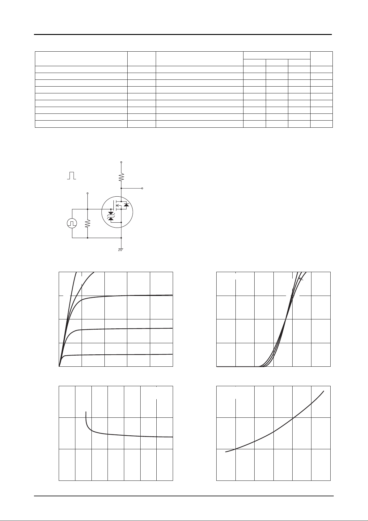
Switching Time Test Circuit
VDD=100V
V
IN
10V
0V
PW=10µs
D.C.≤1%
V
IN
ID=10A
RL=10Ω
D
V
OUT
Ratings
min typ max
Unit
G
P.G
40
50Ω
ID -- V
S
2SK2379
DS
5.0V
=10.0V
30
GS
V
-- A
D
20
4.0V
3.5V
Drain Current, I
10
3.0V
0
048121620
150
Drain-to-Source V oltage, VDS -- V
RDS(on) -- V
GS
IT01936
Tc=25°C
ID=10A
40
VDS=10V
30
-- A
D
20
Drain Current, I
10
0
023 6541
Gate-to-Source V oltage, VGS -- V
150
VGS=10V
ID=10A
ID -- V
GS
RDS(on) -- Tc
Tc= --25°C
25°C
75°C
IT01937
100
(on) -- mΩ
DS
50
Static Drain-to-Source
On-State Resistance, R
0
Gate-to-Source V oltage, VGS -- V
IT01938
100
(on) -- mΩ
DS
50
Static Drain-to-Source
On-State Resistance, R
0
--80 800 40 160120--40048122 6 10 14
Case Temperature, Tc -- °C
IT01939
No.5374-2/4
 Loading...