

Sanyo 2SK1459LS Specifications
Ordering number : ENN3462B
2SK1459LS
N-Channel Silicon MOSFET
2SK1459LS
Ultrahigh-Speed Switching Applications
Features
•
Low ON-resistance.
•
Ultrahigh-speed switching.
•
Micaless package facilitating mounting.
Specifications
Absolute Maximum Ratings at T a=25°C
Parameter Symbol Conditions Ratings Unit
Drain-to-Source Voltage V
Gate-to-Source Voltage V
Drain Current (DC) I
Drain Current (Pulse) I
Allowable Power Dissipation P
Channel T emperature T ch 150 °C
Storage T emperature Tstg --55 to +150 °C
DSS
GSS
D
DP
D
PW≤10µs, duty cycle≤1% 5 A
Tc=25°C30W
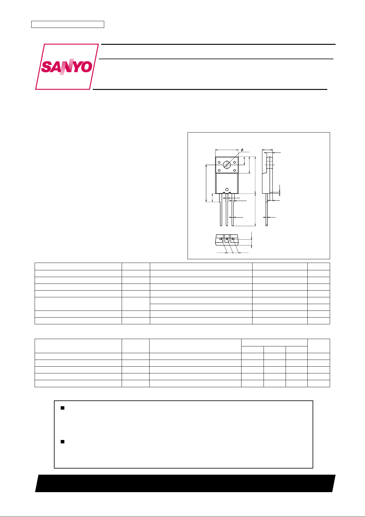
Package Dimensions
unit : mm
2078C
[2SK1459LS]
10.0
16.1
3.6
123
2.55
0.9
0.75
1.2
2.55
3.2
3.5
7.2
16.0
14.0
2.4
4.5
2.8
0.6
1.2
0.7
1 : Gate
2 : Drain
3 : Source
SANYO : TO-220FI(LS)
900 V
±30 V
2.5 A
2.0 W
Electrical Characteristics at Ta=25°C
Parameter Symbol Conditions
Drain-to-Source Breakdown Voltage V
Zero-Gate Voltage Drain Current I
Gate-to-Source Leakage Current I
Cutoff Voltage VGS(off) VDS=10V, ID=1mA 2.0 3.0 V
Forward Transfer Admittance
(BR)DSSID
DSS
GSS
yfs
=1mA, VGS=0 900 V
VDS=900V, VGS=0 1.0 mA
VGS=±30V, VDS=0 ±100 nA
VDS=20V, ID=1.5A 0.8 1.5 S
min typ max
Marking : K1459 Continued on next page.
Any and all SANYO products described or contained herein do not have specifications that can handle
applications that require extremely high levels of reliability, such as life-support systems, aircraft's
control systems, or other applications whose failure can be reasonably expected to result in serious
physical and/or material damage. Consult with your SANYO representative nearest you before using
any SANYO products described or contained herein in such applications.
SANYO assumes no responsibility for equipment failures that result from using products at values that
exceed, even momentarily, rated values (such as maximum ratings, operating condition ranges, or other
parameters) listed in products specifications of any and all SANYO products described or contained
herein.
Ratings
Unit
SANYO Electric Co.,Ltd. Semiconductor Company
TOKYO OFFICE Tokyo Bldg., 1-10, 1 Chome, Ueno, Taito-ku, TOKYO, 110-8534 JAPAN
N3001 TS IM TA-3433 / 61599 TH (KT) / 72597 TS (KOTO) / 6131 JN (KOTO)
No.3462-1/4
2SK1459LS
Continued from preceding page.
Parameter Symbol Conditions
Static Drain-to-Source On-State Resistance RDS(on) ID=1.5A, VGS=10V 4.7 60 Ω
Input Capacitance Ciss VDS=20V , f=1MHz 350 pF
Output Capacitance Coss VDS=20V , f=1MHz 150 pF
Reverse Transfer Capacitance Crss VDS=20V , f=1MHz 100 pF
Turn-ON Delay Time td(on) ID=1.5A, VGS=10V, VDD=200V, RGS=50Ω 15 ns
Rise Time t
Turn-OFF Delay Time td(off) ID=1.5A, VGS=10V, VDD=200V, RGS=50Ω 120 ns
Fall Time t
Diode Forward Voltage V
SD
ID=1.5A, VGS=10V, VDD=200V, RGS=50Ω 25 ns
r
ID=1.5A, VGS=10V, VDD=200V, RGS=50Ω 40 ns
f
IS=2.5A, VGS=0 1.8 V
min typ max
(Note) Be careful in handling the 2SK1459LS because it has no protection diode between gate and source.
Ratings
Unit
Switching Time Test Circuit
V
GS
4
3
-- A
D
2
Drain Current, I
1
PW=1µs
D.C .≤0.5%
P.G
I
D
10V
R
50Ω
-- V
G
GS
DS
V
DD
200V
D
S
GS
V
ID=1.5A
RL=133Ω
2SK1459LS
10V
=
6V
5V
4V
V
OUT
6
5
-- A
4
D
3
2
Drain Current, I
1
I
D
-- V
V
DS
GS
=
10V
6V
5V
4V
0
0
5
4
-- A
D
3
2
Drain Current, I
1
0
0
1248 2416 20
Drain-to-Source V oltage, V
I
-- V
D
°C
--25
Tc=
2861210 144
Gate-to-Source V oltage, V
GS
DS
GS
-- V
25°C
75°C
-- V
ITR01582
VDS=20V
ITR01584
0
0
5
4
-- A
D
3
2
Drain Current, I
1
0
--60 --40 --20
3010 20 6040 50
Drain-to-Source V oltage, V
I
-- Tc
D
V
2006040 16014012010080
Case Temperature, Tc -- °C
DS
10V
DS
=20V
-- V
VGS=10V
ITR01583
ITR01585
No.3462-2/4
 Loading...