

Sanyo 2SK1457 Specifications
Any and all SANYO products described or contained herein do not have specifications that can handle
applications that require extremely high levels of reliability, such as life-support systems, aircraft’s
control systems, or other applications whose failure can be reasonably expected to result in serious
physical and/or material damage. Consult with your SANYO representative nearest you before using
any SANYO products described or contained herein in such applications.
SANYO assumes no responsibility for equipment failures that result from using products at values that
exceed, even momentarily, rated values (such as maximum ratings, operating condition ranges,or other
parameters) listed in products specifications of any and all SANYO products described or contained
herein.
N-Channel Silicon MOSFET
Ultrahigh-Speed Switching Applications
Ordering number:EN3460
2SK1457
SANYO Electric Co.,Ltd. Semiconductor Company
TOKYO OFFICE Tokyo Bldg., 1-10, 1 Chome, Ueno, Taito-ku, TOKYO, 110-8534 JAPAN
10.2
18.0
Features
· Low ON-state resistance.
· Ultrahigh-speed switching.
· Converters.
Specifications
Absolute Maximum Ratings at Ta = 25˚C
retemaraPlobmySsnoitidnoCsgnitaRtinU
egatloVecruoS-ot-niarDV
egatloVecruoS-ot-etaGV
)CD(tnerruCniarDI
)esluP(tnerruCniarDI
noitapissiDrewoPelbawollAP
erutarepmeTlennahChcT 051
erutarepmeTegarotSgtsT 051+ot55–
D
PD
D
SSD
SSG
PW≤10µs, duty cycle≤1%
Tc=25°C
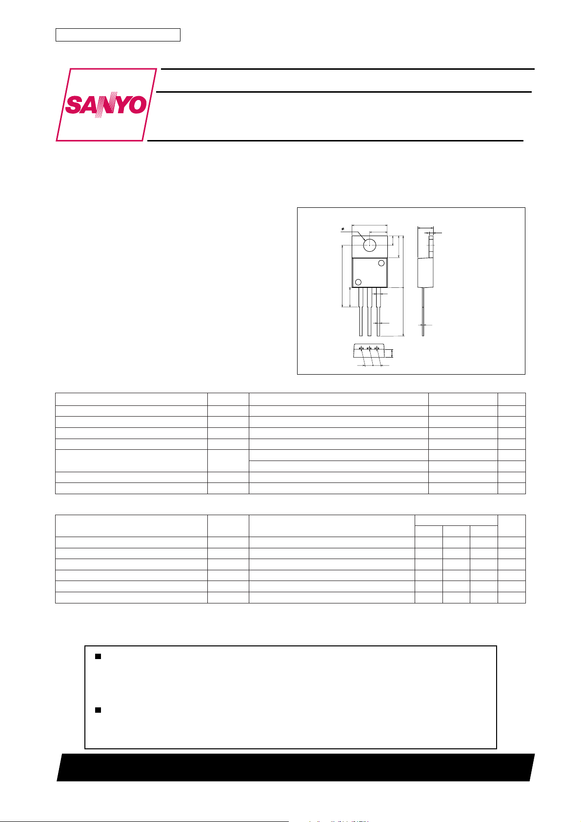
Package Dimensions
unit:mm
2052C
[2SK1457]
3.6
5.6
2.55
5.1
123
2.7
6.3
15.1
1.2
14.0
0.8
2.7
2.55
4.5
1.3
1 : Gate
0.4
2 : Drain
3 : Source
EIAJ : SC-46
SANYO : TO-220AB
009V
03±V
5A
01A
07W
57.1W
˚C
˚C
Electrical Characteristics at Ta = 25˚C
retemaraPlobmySsnoitidnoC
egatloVnwodkaerBecruoS-ot-niarDV
tnerruCniarDegatloVetaG-oreZI
tnerruCegakaeLecruoS-ot-etaGI
egatloVffotuCV
ecnattimdArefsnarTdrawroF|sfy|VSDI,V02=
ecnatsiseRetatS-NOecruoS-ot-niarDcitatSR
I
V,Am1=
SSD)RB(
D
V
SSD
SSG
SD
V
SG
V
)ffo(SG
SD
I
)no(SD
D
0=009V
SG
V,V009=
0=0.1Am
SG
V,V03±=
0=001±An
SD
I,V01=
Am1=0.20.3V
D
A2=0.10.2S
D
V,A2=
V01=8.26.3
SG
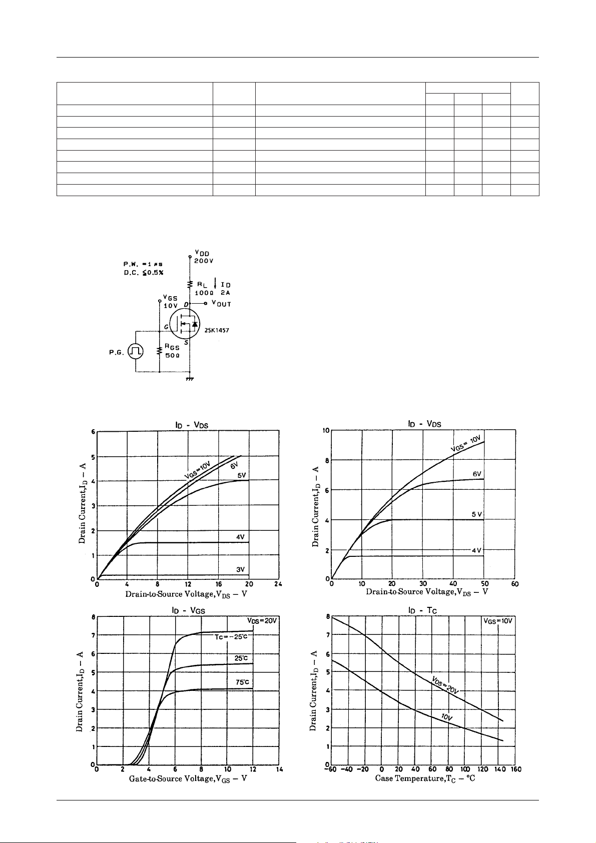
(Note) Be careful in handling the 2SK1457 because it has no protection diode between gate and source. Continued on next page.
61099TH (KT)/6131JN (KOTO) X-6826, 8035 No.3460–1/4
nimpytxam
sgnitaR
tinU
Ω
2SK1457
Continued from preceding page.
retemaraPlobmySsnoitidnoC
ecnaticapaCtupnIssiCV
ecnaticapaCtuptuOssoCV
ecnaticapaCrefsnarTesreveRssrCV
emiTyaleDNO-nruTt
emiTesiRt
emiTyaleDFFO-nruTt
emiTllaFt
egatloVdrawroFedoiDV
r
f
DS
SD
SD
SD
I
)no(d
)ffo(d
V,A2=
D
I
V,A2=
D
I
V,A2=
D
I
V,A2=
D
I
V,A5=
S
Switching Time Test Circuit
zHM1=f,V02=007Fp
zHM1=f,V02=003Fp
zHM1=f,V02=071Fp
V,V01=
SG
SG
SG
SG
SG
DD
V,V01=
DD
V,V01=
DD
V,V01=
DD
0=8.1V
nimpytxam
R,V002=
05= Ω 51sn
SG
R,V002=
05= Ω 53sn
SG
R,V002=
05= Ω 002sn
SG
R,V002=
05= Ω 56sn
SG
sgnitaR
tinU
No.3460–2/4
 Loading...