

SANYO 2SJ400 Datasheet
Any and all SANYO products described or contained herein do not have specifications that can handle
applications that require extremely high levels of reliability, such as life-support systems, aircraft’s
control systems, or other applications whose failure can be reasonably expected to result in serious
physical and/or material damage. Consult with your SANYO representative nearest you before using
any SANYO products described or contained herein in such applications.
SANYO assumes no responsibility for equipment failures that result from using products at values that
exceed, even momentarily, rated values (such as maximum ratings, operating condition ranges,or other
parameters) listed in products specifications of any and all SANYO products described or contained
herein.
P-Channel Silicon MOSFET
Ultrahigh-Speed Switching Applications
Ordering number:ENN6422
2SJ400
SANYO Electric Co.,Ltd. Semiconductor Company
TOKYO OFFICE Tokyo Bldg., 1-10, 1 Chome, Ueno, Taito-ku, TOKYO, 110-8534 JAPAN
9.93.0
20.9
4.5
Features
· Low ON resistance.
· Ultrahigh-speed switching.
· 4V drive.
· Enables simplified fabrication, high-density mounting, and miniaturization in end products due to the
surface mountable package.
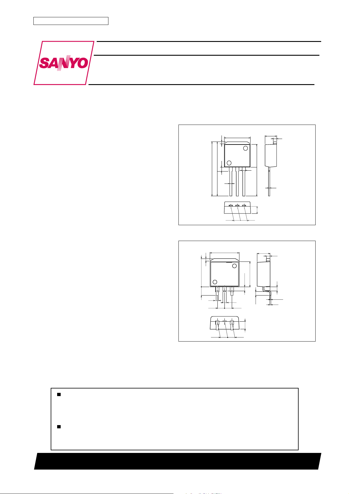
Package Dimensions
unit:mm
2093A
[2SJ400]
10.2
0.9
11.5
unit:mm
2090A
1.6
0.8
9.4
2.55
10.2
0.8
1.2
123
[2SJ400]
2.55
1.3
11.0 8.8
0.4
1 : Gate
2.7
4.5
2 : Drain
3 : Source
SANYO : SMP
1.3
8.8
1.5max
123
0.8
2.55
1.2
2.55
2.7
2.552.55
30300TS (KOTO) TA-2164 No.6422–1/4
1.35
1.4
0 to 0.3
0.4
1 : Gate
2 : Drain
3 : Source
SANYO : SMP-FD
2SJ400
Specifications
Absolute Maximum Ratings at Ta = 25˚C
retemaraPlobmySsnoitidnoCsgnitaRtinU
egatloVecruoS-ot-niarDV
egatloVecruoS-ot-etaGV
)CD(tnerruCniarDI
)esluP(tnerruCniarDI
noitapissiDrewoPelbawollAP
erutarepmeTlennahChcT 051
erutarepmeTegarotSgtsT 051+ot55–
Electrical Characteristics at Ta = 25˚C
retemaraPlobmySsnoitidnoC
egatloVnwodkaerBecruoS-ot-niarDV
egatloVnwodkaerBecruoS-ot-etaGV
tnerruCniarDegatloVetaG-oreZI
tnerruCegakaeLecruoS-ot-etaGI
egatloVffotuCV
ecnattimdArefsnarTdrawroF|sfy|VSDI,V01–=
ecnatsiseRetatS-nOecruoS-ot-niarDcitatS
ecnaticapaCtupnIssiCV
ecnaticapaCtuptuOssoCV
ecnaticapaCrefsnarTesreveRssrCV
emiTyaleDNO-nruTt
emiTesiRt
emiTyaleDFFO-nruTt
emiTllaFt
egatloVdrawroFedoiDV
SSD
SSG
D
PW≤10µs, duty cycle≤1%
PD
D
Tc=25˚C
I
SSD)RB(
D
I
SSG)RB(
G
V
SSD
V
SSG
)ffo(VSDI,V01–=
SG
RSD)no(IDV,A81–=
RSD)no(IDV,A81–=
)no(d
r
)ffo(d
f
I
DS
S
V,Am1–=
0=03–V
SG
V,Aµ001±=
0=02±V
SD
V,V03–=
SD
SG
SD
SD
SD
0=001–Aµ
SG
V,V61±=
0=01±Aµ
SD
Am1–=0.1–0.2–V
D
A81–=6172S
D
V01–=0203mΩ
SG
V4–=0304mΩ
SG
zHM1=f,V01–=0004Fp
zHM1=f,V01–=0042Fp
zHM1=f,V01–=088Fp
tiucriCtseTdeificepseeS03sn
tiucriCtseTdeificepseeS002sn
tiucriCtseTdeificepseeS005sn
tiucriCtseTdeificepseeS072sn
V,A53–=
0=0.1–5.1–V
SG
sgnitaR
nimpytxam
03–V
02±V
53–A
041–A
56.1W
07W
˚C
˚C
tinU
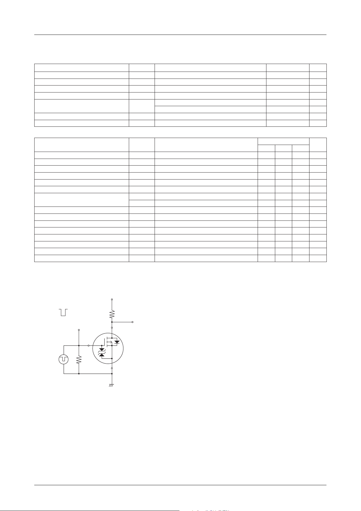
Switching Time Test Circuit
VDD=--30V
V
in
0V
--10V
V
in
PW=10µs
D.C.≤1%
P.G
G
50Ω
ID=--18A
RL=1.67Ω
D
2SJ400
S
V
OUT
No.6422–2/4
 Loading...