

Any and all SANYO products described or contained herein do not have specifications that can handle
applications that require extremely high levels of reliability, such as life-support systems, aircraft’s
control systems, or other applications whose failure can be reasonably expected to result in serious
physical and/or material damage. Consult with your SANYO representative nearest you before using
any SANYO products described or contained herein in such applications.
SANYO assumes no responsibility for equipment failures that result from using products at values that
exceed, even momentarily, rated values (such as maximum ratings, operating condition ranges,or other
parameters) listed in products specifications of any and all SANYO products described or contained
herein.
P-Channel Silicon MOSFET
Ultrahigh-Speed Switching Applications
Ordering number:ENN6396
2SJ339
SANYO Electric Co.,Ltd. Semiconductor Company
TOKYO OFFICE Tokyo Bldg., 1-10, 1 Chome, Ueno, Taito-ku, TOKYO, 110-8534 JAPAN
18.1
4.5
Features
· Low ON resistance.
· Ultrahigh-speed switching.
· 4V drive.
· Micaless package facilitating mounting.
Specifications
Absolute Maximum Ratings at Ta = 25˚C
retemaraPlobmySsnoitidnoCsgnitaRtinU
egatloVecruoS-ot-niarDV
egatloVecruoS-ot-etaGV
)CD(tnerruCniarDI
)esluP(tnerruCniarDI
noitapissiDrewoPelbawollAP
erutarepmeTlennahChcT 051
erutarepmeTegarotSgtsT 051+ot55–
D
D
SSD
SSG
PW≤10µs, duty cycle≤1%
PD
Tc=25˚C
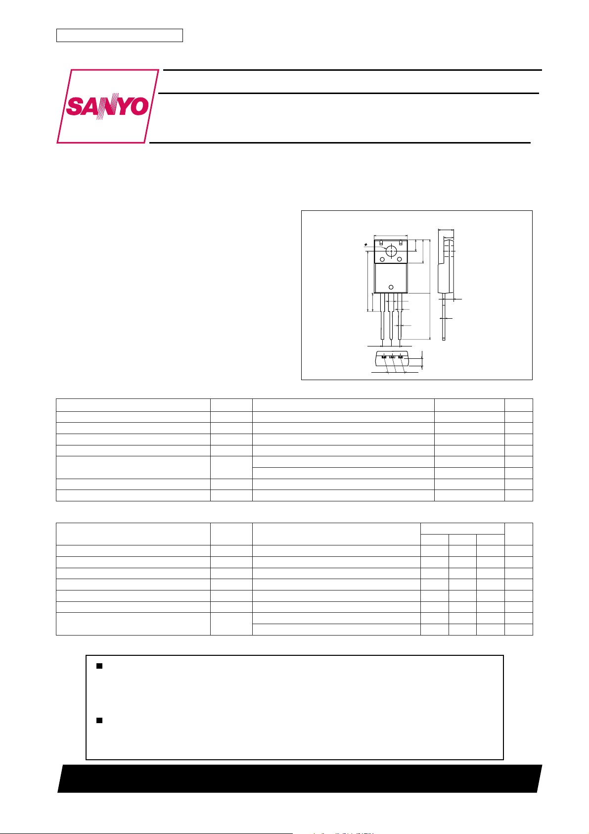
Package Dimensions
unit:mm
2063A
[2SJ339]
10.0
3.2
5.6
1
2.55
2.55
3.5
1.6
1.2
0.75
23
2.55
2.55
2.8
7.2
16.0
2.4
0.7
14.0
1 : Gate
2.4
2 : Drain
3 : Source
SANYO : TO-220ML
06–V
02±V
52–A
001–A
2W
04W
˚C
˚C
Electrical Characteristics at Ta = 25˚C
retemaraPlobmySsnoitidnoC
egatloVnwodkaerBecruoS-ot-niarDV
egatloVnwodkaerBecruoS-ot-etaGV
tnerruCniarDegatloVetaG-oreZI
tnerruCegakaeLecruoS-ot-etaGI
egatloVffotuCV
ecnattimdArefsnarTdrawroF|sfy|VSDI,V01–=
ecnatsiseRetatS-nOecruoS-ot-niarDcitatSR
SSD
SSG
SG
SD
I
SSD)RB(
D
I
SSG)RB(
G
V
SD
V
SG
)ffo(VSDI,V01–=
I
D
)no(
I
D
V,Am1–=
0=06–V
SG
V,Aµ001±=
0=02±V
SD
V,V06–=
0=001–Aµ
SG
V,V61±=
0=01±Aµ
SD
Am1–=0.1–0.2–V
D
A51–=5152S
D
V,A51–=
V,A51–=
V01–=0304mΩ
SG
V4–=0455mΩ
SG
30300TS (KOTO) TA-2177 No.6396–1/4
sgnitaR
nimpytxam
Continued on next page.
tinU
2SJ339
Continued from preceding page.
retemaraPlobmySsnoitidnoC
ecnaticapaCtupnIssiCV
ecnaticapaCtuptuOssoCV
ecnaticapaCrefsnarTesreveRssrCV
emiTyaleDNO-nruTt
emiTesiRt
emiTyaleDFFO-nruTt
emiTllaFt
egatloVdrawroFedoiDV
r
f
DS
SD
SD
SD
)no(d
)ffo(d
I
S
Switching Time Test Circuit
VDD=--30V
V
0V
--10V
PW=10µs
D.C.≤1%
P.G
IN
V
IN
G
50Ω
ID=--15A
RL=2Ω
D
S
V
OUT
zHM1=f,V02–=0083Fp
zHM1=f,V02–=0021Fp
zHM1=f,V02–=003Fp
tiucriCtseTdeificepseeS03sn
tiucriCtseTdeificepseeS051sn
tiucriCtseTdeificepseeS054sn
tiucriCtseTdeificepseeS022sn
V,A52–=
0=0.1–5.1–V
SG
sgnitaR
nimpytxam
tinU
--50
--40
–A
D
--30
--20
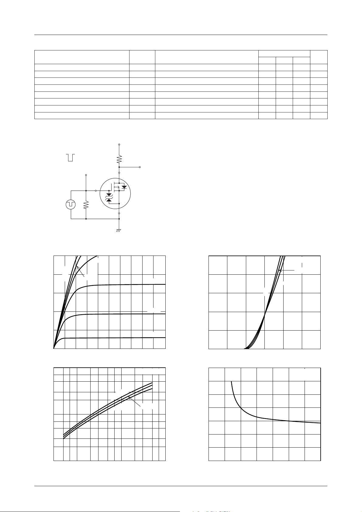
Drain Current, I
--10
100
fs|–S
y
10
Forward Transfer Admittance, |
1.0
I
=--5.0V
GS
V
--4.0V
--4.5V
D
-- V
DS
--3.5V
--3.0V
--50
--40
–A
D
--30
--20
I
D
-- V
Tc=--25°C
GS
VDS=--10V
25°C
75°C
Drain Current, I
--2.5V
0
0
7
5
3
2
7
5
3
2
3
--2--1 --3 --5 --7 --9--4 --8 --10--6
Drain-to-Source Voltage, VDS–V
yfs -- I
D
IT00661
VDS=--10V
°C
Tc=--25
75°C
23 5 3 57
--1.0
Drain Current, ID– A Gate-to-Source Voltage, VGS–V
25°C
2757
--10 --100
IT00663
--10
0
0
Gate-to-Source Voltage, VGS–V
70
60
50
–mΩ
(on)
40
DS
30
20
10
Static Drain-to-Source
On-State Resistance, R
0
0
--2--1 --3 --5 --6--4
RDS(on) -- V
--8--2 --12 --14--6 --10--4
IT00662
GS
Tc=25°C
ID=--15A
IT00664
No.6396–2/4
 Loading...