

Sanyo 2SJ257 Specifications
Any and all SANYO products described or contained herein do not have specifications that can handle
applications that require extremely high levels of reliability, such as life-support systems, aircraft’s
control systems, or other applications whose failure can be reasonably expected to result in serious
physical and/or material damage. Consult with your SANYO representative nearest you before using
any SANYO products described or contained herein in such applications.
SANYO assumes no responsibility for equipment failures that result from using products at values that
exceed, even momentarily, rated values (such as maximum ratings, operating condition ranges,or other
parameters) listed in products specifications of any and all SANYO products described or contained
herein.
P-Channel Silicon MOSFET
Ultrahigh-Speed Switching Applications
Ordering number:EN4242
2SJ257
SANYO Electric Co.,Ltd. Semiconductor Company
TOKYO OFFICE Tokyo Bldg., 1-10, 1 Chome, Ueno, Taito-ku, TOKYO, 110-8534 JAPAN
9.93.0
Features
· Low ON resistance.
· Ultrahigh-speed switching.
· Low-voltage drive.
· Surface mount type device making the following
possible.
· Reduction in the number of manufacturing processes for 2SJ257-applied equipment.
· High density surface mount applications.
· Small size of 2SJ257-applied equipment.
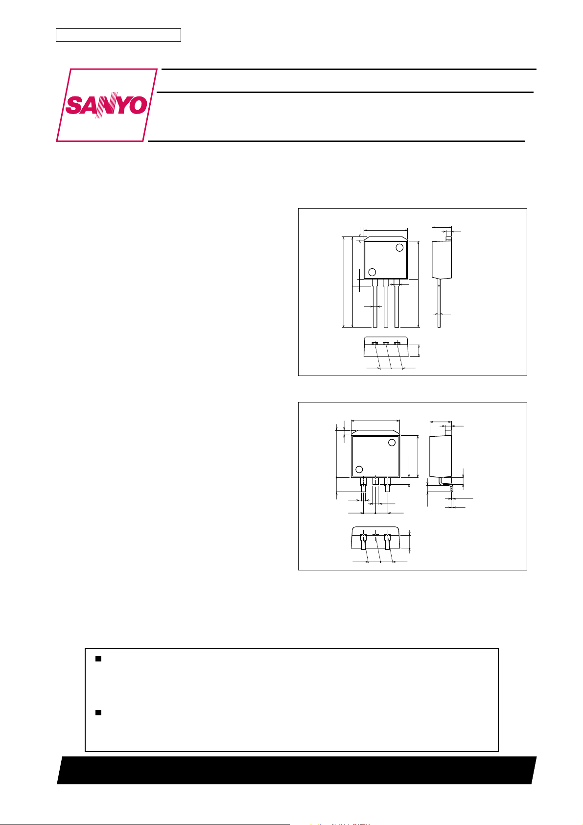
Package Dimensions
unit:mm
2093A
[2SJ257]
10.2
0.9
11.5
unit:mm
2090A
20.9
0.8
1.6
0.8
9.4
2.55
10.2
1.2
123
2.55
[2SJ257]
4.5
1.3
11.0 8.8
0.4
1 : Gate
2.7
4.5
2 : Drain
3 : Source
SANYO : SMP
1.3
8.8
123
0.8
2.55
1.5max
1.2
2.55
2.552.55
1.35
2.7
1.4
0 to 0.3
0.4
1 : Gate
2 : Drain
3 : Source
SANYO : SMP-FD
42899TH (KT)/51193TH (KOTO) AX-8376 No.4242–1/4
2SJ257
Specifications
Absolute Maximum Ratings at Ta = 25˚C
retemaraPlobmySsnoitidnoCsgnitaRtinU
egatloVecruoS-ot-niarDV
egatloVecruoS-ot-etaGV
)CD(tnerruCniarDI
)esluP(tnerruCniarDI
noitapissiDrewoPelbawollAP
erutarepmeTlennahChcT 051
erutarepmeTegarotSgtsT 051+ot55–
Electrical Characteristics at Ta = 25˚C
retemaraPlobmySsnoitidnoC
egatloVnwodkaerBecruoS-ot-niarDV
egatloVnwodkaerBecruoS-ot-etaGV
tnerruCniarDegatloVetaG-oreZI
tnerruCegakaeLecruoS-ot-etaGI
egatloVffotuCV
ecnattimdArefsnarTdrawroF|sfy|VSDI,V01–=
ecnatsiseRetatS-NOecruoS-ot-niarDcitatS
ecnaticapaCtupnIssiCV
ecnaticapaCtuptuOssoCV
ecnaticapaCrefsnarTesreveRssrCV
emiTyaleDNO-nruTt
emiTesiRt
emiTyaleDFFO-nruTt
emiTllaFt
egatloVdrawroFedoiDV
SSD
SSG
D
PW≤10µs, duty cycle≤1%
PD
D
Tc=25°C
I
SSD)RB(
D
I
SSG)RB(
G
V
SSD
V
SSG
V
)ffo(SG
R
R
I
)no(SD
D
I
)no(SD
D
)no(d
r
)ffo(d
f
I
DS
S
V,Am1–=
0=03–V
SG
V,Aµ001±=
0=51±V
SD
V,V03–=
SD
SG
SD
V,A5–=
V,A5–=
SD
SD
SD
0=001–Aµ
SG
V,V21±=
0=01±Aµ
SD
I,V01–=
Am1–=0.1–0.2–V
D
A5–=45.6S
D
V01–=58021mΩ
SG
V4–=021071mΩ
SG
zHM1=f,V01–=0001Fp
zHM1=f,V01–=006Fp
zHM1=f,V01–=022Fp
tiucriCtseTdeificepseeS51sn
tiucriCtseTdeificepseeS08sn
tiucriCtseTdeificepseeS021sn
tiucriCtseTdeificepseeS071sn
V,A01–=
0=0.1–5.1–V
SG
sgnitaR
nimpytxam
03–V
51±V
01–A
04–A
56.1W
05W
˚C
˚C
tinU
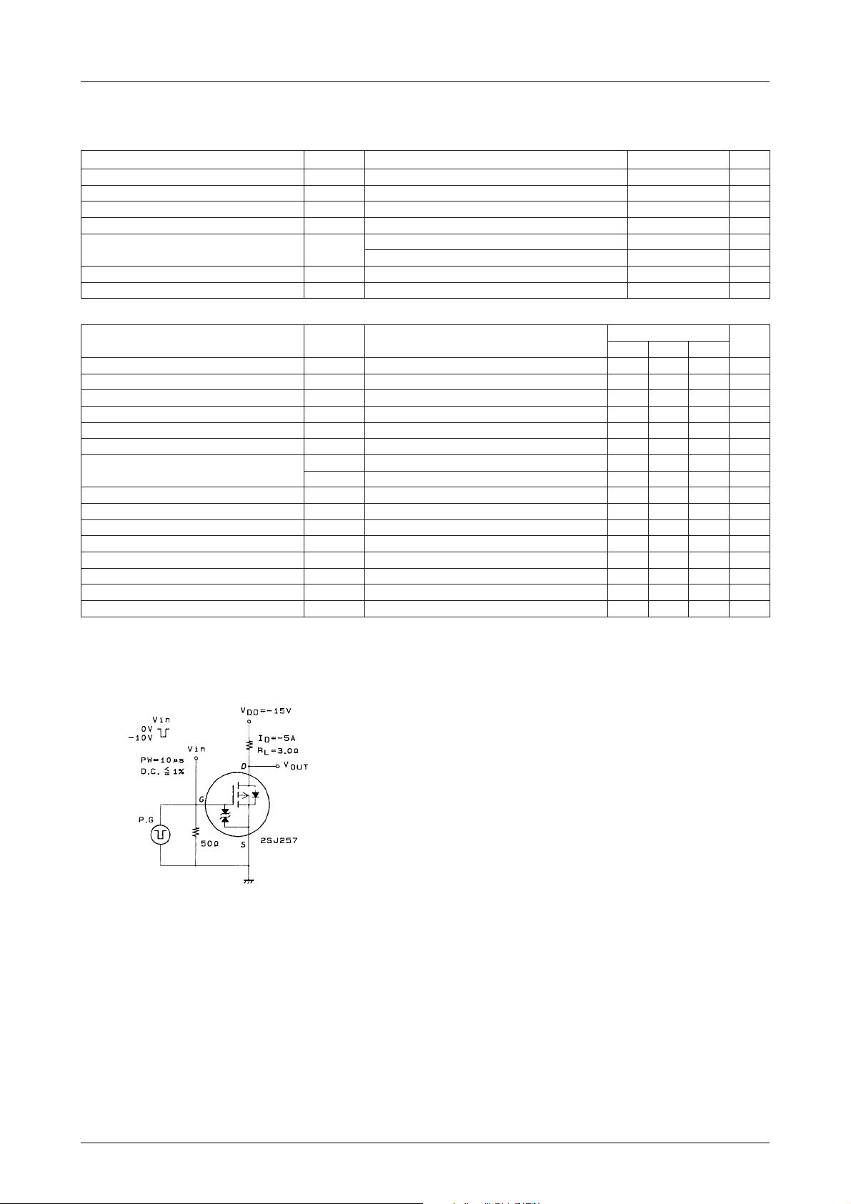
Switching Time Test Circuit
No.4242–2/4
 Loading...