

SANYO 2SD2646 Datasheet
Ordering number : ENN6922
2SD2646
NPN Triple Diffused Planar Silicon Transistor
2SD2646
Color TV Horizontal Deflection
Output Applications
Features
•
High speed.
• High breakdown voltage(V
• High reliability(Adoption of HVP process).
• Adoption of MBIT process.
CBO
=1500V).
Specifications
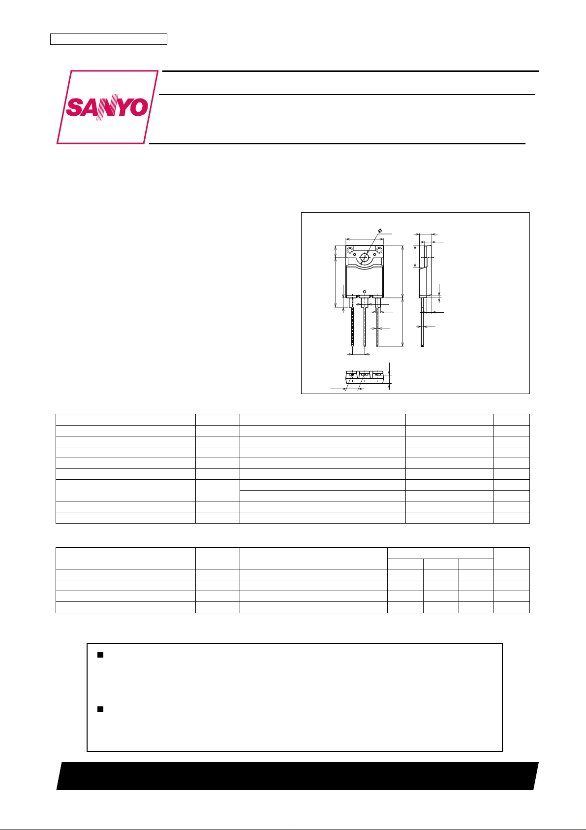
Package Dimensions
unit : mm
2174A
[2SD2646]
3.4
16.0
5.0
2.8
0.7
22.0
2.0
20.4
3.5
21.0
5.45
4.0
123
5.45
5.6
3.1
8.0
0.8
2.1
0.9
1 : Base
2 : Collector
3 : Emitter
SANYO : TO-3PMLH
Absolute Maximum Ratings at T a=25°C
Parameter Symbol Conditions Ratings Unit
Collector-to-Base Voltage V
Collector-to-Emitter Voltage V
Emitter-to-Base Voltage V
Collector Current I
Collector Current (Pulse) I
Collector Dissipation P
Junction T emperature Tj 150 ° C
Storage T emperature T stg --55 to +150 °C
CBO
CEO
EBO
C
CP
C
Tc=25°C80W
1500 V
700 V
5V
10 A
25 A
3.0 W
Electrical Characteristics at Ta=25°C
Parameter Symbol Conditions
Collector Cutoff Current I
Collector Cutoff Current I
Collector Sustain Voltage V
Emitter Cutoff Current I
CBO
CES
CEO
EBO
Any and all SANYO products described or contained herein do not have specifications that can handle
applications that require extremely high levels of reliability, such as life-support systems, aircraft's
control systems, or other applications whose failure can be reasonably expected to result in serious
physical and/or material damage. Consult with your SANYO representative nearest you before using
any SANYO products described or contained herein in such applications.
SANYO assumes no responsibility for equipment failures that result from using products at values that
exceed, even momentarily, rated values (such as maximum ratings, operating condition ranges, or other
parameters) listed in products specifications of any and all SANYO products described or contained
herein.
SANYO Electric Co.,Ltd. Semiconductor Company
TOKYO OFFICE Tokyo Bldg., 1-10, 1 Chome, Ueno, Taito-ku, TOKYO, 110-8534 JAPAN
Ratings
min typ max
VCB=800V, IE=0 10 µA
VCE=1500V , RBE=0 1.0 mA
(sus) IC=100mA, IB=0 700 V
VBE=4V, IC=0 1.0 mA
Unit
Continued on next page.
62501 TS IM TA-3089
No.6922-1/4
2SD2646
Continued from preceding page.
Parameter Symbol Conditions
Collector-to-Emitter Saturation Voltage VCE(sat) IC=7.2A, IB=1.44A 3 V
Base-to-Emitter Saturation Voltage VBE(sat) IC=7.2A, IB=1.44A 1.5 V
DC Current Gain
Fall Time t
hFE1VCE=5V, IC=1A 15
hFE2VCE=5V, IC=8A 5 8
IC=5A, IB1=1A, IB2=--2A 0.3 µs
f
min typ max
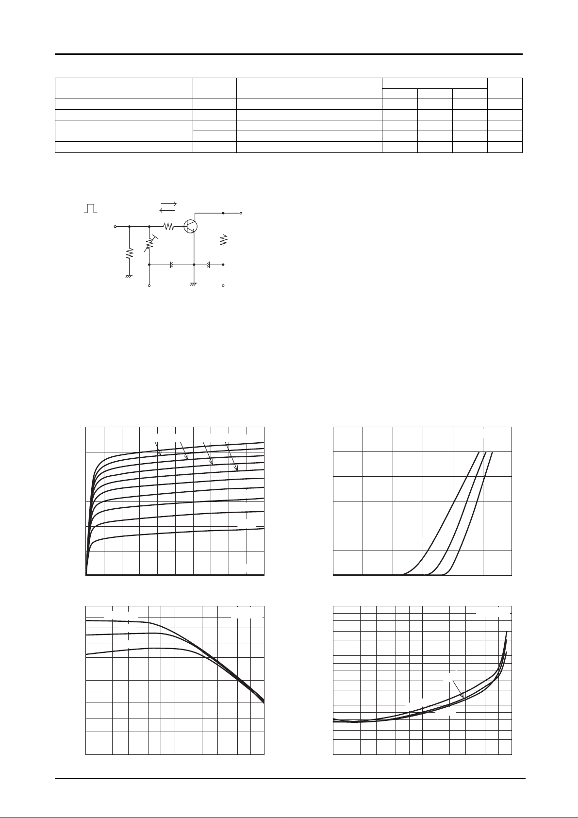
Switching Time Test Circuit
I
PW=20µs
D.C.≤1%
B1
I
B2
OUTPUT
Ratings
Unit
12
10
-- A
C
INPUT
50Ω
8
6
4
V
R
I
C
1.8A
R
B
+
100µF 470µF
-- V
1.6A
+
VCC=200VVBE= --2V
CE
1.4A
1.2A
Collecotr Current, I
2
0
01 3 5 7 9
2468
Collector-to-Emitter Voltage, VCE -- V
h
-- I
100
FE
DC Current Gain, h
1.0
Ta=120°C
7
5
3
2
10
7
5
3
2
0.1 1.0 10
°C
25
°
--40
23 57 23 57
FE
C
C
Collector Current, IC -- A
R
L
40.0Ω
I
-- V
12
C
BE
2.0A
10
1.0A
0.8A
0.6A
0.4A
0.2A
I
=0
B
10
IT03004
VCE=5V
IT03006 IT03007
-- A
8
C
6
4
Collector Current, I
2
0
10
7
5
3
2
1.0
(sat) -- V
7
CE
5
3
2
0.1
7
5
3
Collector-to-Emitter
Saturation V oltage, V
2
0.01
0.1
C
°
C
°
C
°
25
Ta=120
0.20 0.4 0.6 0.8 1.0 1.2
--40
Base-to-Emitter V oltage, VBE -- V
VCE(sat) -- I
C
°C
25
Ta=120°C
--40°C
23 57 23 57
Collector Current, IC -- A
1.0 10
VCE=5V
IT03005
IC / IB=5
No.6922-2/4
 Loading...